Comparing Dielectric Constants in Nanosheet Compositions
APR 23, 20269 MIN READ
Generate Your Research Report Instantly with AI Agent
PatSnap Eureka helps you evaluate technical feasibility & market potential.
Nanosheet Dielectric Research Background and Objectives
Nanosheets represent a revolutionary class of two-dimensional materials that have emerged as critical components in next-generation electronic and energy storage applications. These atomically thin structures, typically ranging from single atomic layers to several nanometers in thickness, exhibit unique dielectric properties that differ significantly from their bulk counterparts. The quantum confinement effects and high surface-to-volume ratios inherent in nanosheet geometries create unprecedented opportunities for tailoring dielectric responses through compositional engineering.
The evolution of nanosheet dielectric research traces back to the groundbreaking isolation of graphene in 2004, which demonstrated that two-dimensional materials could maintain structural stability while exhibiting extraordinary electronic properties. This discovery catalyzed extensive research into other layered materials, including transition metal dichalcogenides, hexagonal boron nitride, and various oxide nanosheets. Each material class brought distinct dielectric characteristics, ranging from metallic conductivity to wide-bandgap insulating behavior.
Contemporary technological demands for miniaturized electronic devices with enhanced performance have intensified the need for precise dielectric constant control. Traditional bulk dielectric materials face fundamental limitations in ultra-thin film applications, where interface effects and quantum size effects become dominant. Nanosheets offer a unique solution by providing atomically precise thickness control while maintaining crystalline quality and enabling compositional tuning through various synthesis approaches.
The primary objective of comparing dielectric constants across different nanosheet compositions centers on establishing comprehensive structure-property relationships that can guide rational material design. This involves systematic investigation of how atomic composition, layer stacking arrangements, defect concentrations, and interfacial interactions influence dielectric responses across frequency ranges relevant to practical applications.
Advanced characterization techniques, including impedance spectroscopy, scanning probe microscopy, and synchrotron-based methods, have enabled unprecedented precision in measuring dielectric properties at the nanoscale. These capabilities support the development of predictive models that correlate compositional parameters with dielectric performance, ultimately accelerating the discovery of optimized nanosheet materials for specific applications.
The strategic importance of this research extends beyond fundamental understanding to encompass critical technological applications including high-density memory devices, flexible electronics, energy storage systems, and quantum computing platforms. Success in this field promises to unlock new paradigms in electronic device design while addressing the growing demand for materials with precisely tailored dielectric properties.
Market Demand for High-Performance Dielectric Nanosheets
The global electronics industry is experiencing unprecedented demand for high-performance dielectric nanosheets, driven by the relentless miniaturization of electronic devices and the pursuit of enhanced performance characteristics. This surge in demand stems from the critical role these materials play in next-generation applications including flexible displays, advanced capacitors, high-frequency communication devices, and energy storage systems.
Consumer electronics manufacturers are increasingly seeking dielectric nanosheets with precisely tunable dielectric constants to meet stringent performance requirements. The smartphone and tablet markets particularly drive demand for ultra-thin, flexible dielectric materials that maintain stable electrical properties across varying environmental conditions. Wearable technology represents another rapidly expanding segment, requiring dielectric nanosheets that combine mechanical flexibility with reliable electrical insulation properties.
The automotive industry's transition toward electric vehicles and autonomous driving systems has created substantial demand for high-performance dielectric materials. Advanced driver assistance systems, electric powertrains, and sophisticated sensor networks require dielectric nanosheets capable of operating reliably under extreme temperature variations and electromagnetic interference conditions. These applications demand materials with specific dielectric constant ranges optimized for signal integrity and power efficiency.
Telecommunications infrastructure modernization, particularly the global rollout of 5G networks, has intensified demand for dielectric nanosheets with precisely controlled electrical properties. Base station equipment, antenna systems, and high-frequency circuit boards require materials that minimize signal loss while maintaining dimensional stability. The transition to higher frequency bands necessitates dielectric materials with lower loss tangents and carefully engineered dielectric constants.
Energy storage applications represent a significant growth driver, with supercapacitors and advanced battery systems requiring dielectric nanosheets that deliver superior energy density and cycling stability. Grid-scale energy storage projects and renewable energy integration systems demand materials capable of withstanding high voltage operations while maintaining consistent performance over extended operational lifespans.
The aerospace and defense sectors continue to drive demand for specialized dielectric nanosheets capable of operating in extreme environments. Satellite communication systems, radar applications, and military electronics require materials with exceptional thermal stability and radiation resistance, often necessitating custom dielectric constant specifications tailored to specific mission requirements.
Current State of Nanosheet Dielectric Constant Measurement
The measurement of dielectric constants in nanosheet compositions has emerged as a critical area of materials characterization, driven by the increasing demand for high-performance electronic devices and energy storage systems. Current measurement techniques encompass both traditional and advanced methodologies, each presenting distinct advantages and limitations when applied to two-dimensional materials.
Impedance spectroscopy remains the most widely adopted technique for dielectric constant measurement in nanosheets. This method involves applying alternating electric fields across frequencies ranging from millihertz to gigahertz, enabling comprehensive characterization of frequency-dependent dielectric behavior. Modern impedance analyzers can achieve measurement accuracies within 1-2% for bulk materials, though precision decreases significantly for ultra-thin nanosheets due to parasitic capacitance effects and contact resistance issues.
Capacitance-voltage profiling has gained prominence for characterizing individual nanosheet layers and heterostructures. This technique measures capacitance changes as a function of applied voltage, providing insights into charge distribution and interface effects. Recent developments in scanning probe microscopy have enabled localized dielectric measurements with nanometer-scale spatial resolution, allowing researchers to map dielectric variations across single nanosheet surfaces.
Terahertz time-domain spectroscopy represents an emerging non-contact measurement approach particularly valuable for studying pristine nanosheet samples. This technique eliminates electrode-related artifacts and enables measurement of intrinsic dielectric properties without sample modification. However, current sensitivity limitations restrict its application to relatively thick nanosheet assemblies or multilayer structures.
Microwave cavity perturbation methods have shown promise for measuring dielectric constants of suspended nanosheets, minimizing substrate interference effects that plague conventional techniques. These methods achieve high sensitivity by detecting frequency shifts in resonant cavities upon sample insertion, though they require careful calibration and are limited to specific frequency ranges.
The primary challenge facing current measurement techniques lies in accurately characterizing ultra-thin nanosheets where surface effects dominate bulk properties. Quantum confinement effects, surface charge states, and environmental interactions significantly influence measured dielectric constants, often leading to substantial deviations from bulk material values. Additionally, sample preparation methods, including transfer techniques and substrate selection, introduce variability that complicates comparative studies across different research groups.
Standardization efforts remain limited, with measurement protocols varying significantly between laboratories. This lack of standardization hampers reliable comparison of dielectric constants across different nanosheet compositions and synthesis methods, highlighting the need for established measurement standards and reference materials in this rapidly evolving field.
Existing Methods for Dielectric Constant Comparison
01 High-k dielectric materials for nanosheet transistors
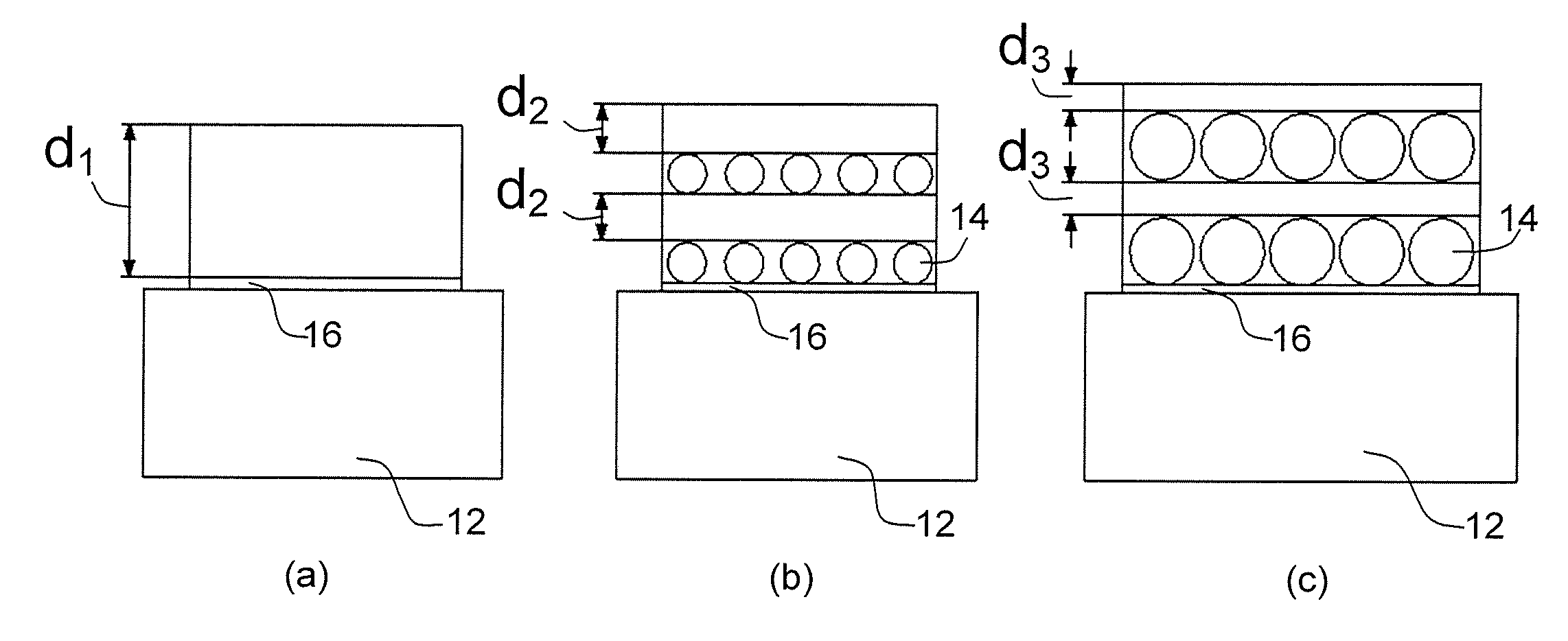
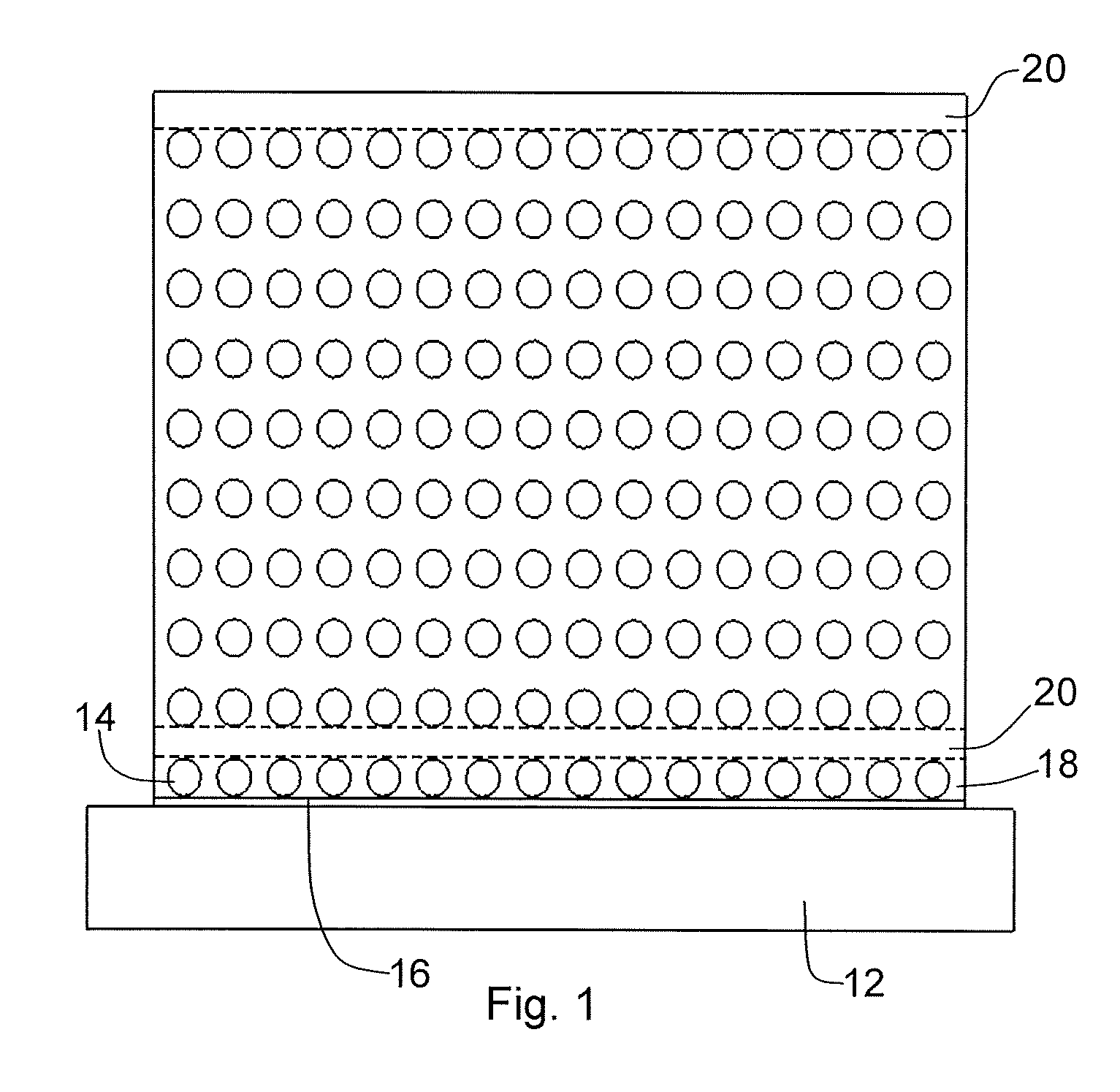
High dielectric constant materials are utilized in nanosheet-based transistor structures to improve gate control and reduce leakage current. These materials include metal oxides and other compounds with dielectric constants significantly higher than silicon dioxide. The integration of high-k dielectrics enables scaling of nanosheet devices while maintaining electrical performance and reducing power consumption.- High-k dielectric materials for nanosheet transistors: High dielectric constant materials are utilized in nanosheet-based transistor structures to improve gate control and reduce leakage current. These materials include metal oxides and other compounds with dielectric constants significantly higher than silicon dioxide. The integration of high-k dielectrics enables scaling of nanosheet devices while maintaining electrical performance and reducing power consumption.
- Two-dimensional material nanosheets with tunable dielectric properties: Two-dimensional nanomaterials such as transition metal dichalcogenides and graphene derivatives exhibit unique dielectric properties that can be tuned through composition control, layer thickness, and chemical modification. These materials demonstrate variable dielectric constants depending on their structural configuration and can be engineered for specific applications in electronic devices and energy storage systems.
- Composite nanosheet structures for enhanced dielectric performance: Composite structures incorporating multiple types of nanosheets or combining nanosheets with polymer matrices achieve enhanced dielectric properties. These composites leverage the synergistic effects between different materials to optimize dielectric constant, breakdown strength, and thermal stability. The layered architecture allows for precise control over electrical properties through material selection and structural design.
- Dielectric constant measurement and characterization methods for nanosheets: Advanced characterization techniques are employed to accurately measure the dielectric constants of nanosheet materials at various frequencies and temperatures. These methods include impedance spectroscopy, capacitance measurements, and non-contact evaluation techniques specifically adapted for thin film and nanostructured materials. Proper characterization is essential for understanding the relationship between nanosheet composition, structure, and dielectric behavior.
- Nanosheet dielectric applications in capacitors and energy storage: Nanosheet materials with optimized dielectric constants are applied in capacitor structures and energy storage devices to achieve high energy density and fast charge-discharge capabilities. The thin geometry and high surface area of nanosheets enable compact device designs with superior performance. Applications include embedded capacitors, supercapacitors, and integrated power delivery systems where space efficiency and electrical performance are critical.
02 Nanosheet compositions with tunable dielectric properties
Nanosheet materials can be engineered with adjustable dielectric constants through compositional modifications and doping strategies. The dielectric properties can be tailored by controlling the thickness, material composition, and layered structure of nanosheets. This tunability allows for optimization of electrical characteristics for specific applications in semiconductor devices and capacitors.Expand Specific Solutions03 Low-k dielectric materials for nanosheet interconnects
Low dielectric constant materials are employed in nanosheet-based interconnect structures to reduce parasitic capacitance and signal delay. These materials include porous structures and organic-inorganic hybrid compositions that minimize dielectric constant while maintaining mechanical stability. The implementation of low-k dielectrics improves signal propagation speed and reduces power dissipation in advanced integrated circuits.Expand Specific Solutions04 Dielectric constant measurement and characterization of nanosheets
Various techniques are employed to measure and characterize the dielectric properties of nanosheet materials at nanoscale dimensions. Methods include capacitance-voltage measurements, impedance spectroscopy, and advanced microscopy techniques. Accurate characterization of dielectric constants is essential for device modeling and optimization of nanosheet-based electronic components.Expand Specific Solutions05 Multilayer nanosheet structures with engineered dielectric interfaces
Multilayer nanosheet architectures incorporate multiple dielectric layers with different dielectric constants to achieve desired electrical characteristics. The interfaces between layers are engineered to minimize defects and optimize charge distribution. These structures enable enhanced device performance through strategic placement of dielectric materials with varying properties, improving both electrical isolation and capacitive coupling control.Expand Specific Solutions
Key Players in Nanosheet and Dielectric Materials Industry
The dielectric constants in nanosheet compositions field represents an emerging technology area in the early development stage, driven by growing demand for advanced electronic materials in semiconductors and energy storage applications. The market shows significant potential with increasing miniaturization requirements across electronics industries. Technology maturity varies considerably among key players, with established corporations like TDK Corp., Panasonic Holdings, and SK Hynix leading in commercial applications and manufacturing capabilities. Research institutions including MIT, KIST Corp., and National Institute for Materials Science drive fundamental innovations, while specialized companies like Nanosys and Pixelligent Technologies focus on niche applications. The competitive landscape features a mix of Japanese electronics giants (TDK, NGK, Hitachi), semiconductor manufacturers (GLOBALFOUNDRIES, SK Hynix), and emerging material specialists, indicating a fragmented but rapidly evolving market with substantial growth opportunities.
TDK Corp.
Technical Solution: TDK has developed advanced multilayer ceramic capacitors (MLCCs) with optimized dielectric constant materials for nanosheet applications. Their technology focuses on barium titanate-based compositions with controlled grain size at nanoscale, achieving dielectric constants ranging from 1000-3000 depending on the specific formulation. The company utilizes proprietary sintering techniques to maintain uniform dielectric properties across ultra-thin layers, enabling reliable performance in high-density electronic applications. Their nanosheet dielectric materials demonstrate excellent temperature stability and low loss characteristics, making them suitable for automotive and industrial electronics where consistent performance is critical.
Strengths: Extensive manufacturing experience and proven reliability in mass production. Weaknesses: Limited flexibility in customizing dielectric constants for specialized applications.
Massachusetts Institute of Technology
Technical Solution: MIT researchers have pioneered computational modeling approaches for predicting dielectric constants in two-dimensional nanosheet materials, particularly focusing on transition metal dichalcogenides and graphene-based composites. Their methodology combines density functional theory calculations with experimental validation to characterize dielectric behavior at the atomic scale. The research team has developed novel measurement techniques using scanning probe microscopy to map dielectric constant variations across individual nanosheets, achieving spatial resolution below 10 nanometers. Their work has established fundamental understanding of how layer thickness, defect density, and interfacial effects influence dielectric properties in nanosheet geometries.
Strengths: Cutting-edge research capabilities and strong theoretical foundation. Weaknesses: Limited commercial scalability and manufacturing readiness of developed technologies.
Core Innovations in Nanosheet Dielectric Property Control
Nano-structured dielectric composite
PatentActiveUS20120003449A1
Innovation
- A multilayer composite structure is created with uniformly distributed nanoparticles embedded in a void-free polymeric dielectric medium, where the size and density of nanoparticles and the thickness of polymer spacer layers are precisely controlled through a vacuum deposition process, ensuring a high dielectric constant and breakdown strength by avoiding nanoparticle agglomeration and gas inclusions.

A NANO sheet comprising niobate dielectric and dielectric thin film comprising the same
PatentActiveKR1020220077989A
Innovation
- Development of niobate dielectric nanosheets with a composition of Sr2(1-x)Bi2xNb3O10, synthesized through cation substitution and a solution deposition process, allowing for the formation of uniform and flat thin films with high dielectric constant and low dielectric loss, even at nano-level thickness.


Environmental Impact of Nanosheet Manufacturing Processes
The manufacturing of nanosheets for dielectric applications presents significant environmental challenges that require comprehensive assessment and mitigation strategies. Traditional synthesis methods, including chemical vapor deposition (CVD), liquid-phase exfoliation, and hydrothermal processes, generate substantial chemical waste and consume considerable energy resources. The production of high-quality nanosheets with precise dielectric properties often involves toxic solvents, heavy metal catalysts, and high-temperature processing conditions that contribute to air and water pollution.
Chemical waste generation represents one of the most pressing environmental concerns in nanosheet manufacturing. Solvent-based exfoliation processes typically require large volumes of organic solvents such as N-methyl-2-pyrrolidone (NMP) and dimethylformamide (DMF), which pose risks to aquatic ecosystems and human health. The disposal and treatment of these chemical byproducts demand sophisticated waste management systems, increasing both operational costs and environmental footprint.
Energy consumption during nanosheet synthesis constitutes another critical environmental factor. High-temperature CVD processes for producing graphene and transition metal dichalcogenide nanosheets require temperatures exceeding 1000°C, resulting in substantial carbon emissions. The energy-intensive nature of these processes directly correlates with greenhouse gas production, particularly when powered by fossil fuel-based electricity grids.
Water usage and contamination present additional environmental challenges. Hydrothermal synthesis methods consume significant quantities of deionized water, while post-processing washing steps generate contaminated wastewater containing nanoparticles and chemical residues. The potential bioaccumulation of nanomaterials in aquatic environments raises concerns about long-term ecological impacts and food chain contamination.
Emerging sustainable manufacturing approaches show promise for reducing environmental impact. Green synthesis methods utilizing bio-compatible solvents, room-temperature processing techniques, and renewable energy integration are being developed to minimize ecological footprint. Closed-loop recycling systems for solvent recovery and advanced filtration technologies for wastewater treatment represent viable pathways toward more environmentally responsible nanosheet production.
The implementation of life cycle assessment (LCA) frameworks enables comprehensive evaluation of environmental impacts from raw material extraction through end-of-life disposal. These assessments guide the development of cleaner production technologies and inform regulatory policies governing nanomaterial manufacturing standards.
Standardization Challenges in Nanosheet Dielectric Testing
The standardization of dielectric testing methodologies for nanosheets presents unprecedented challenges due to the unique physical and electrical properties of two-dimensional materials. Unlike bulk materials, nanosheets exhibit thickness-dependent dielectric behavior that varies significantly at the atomic scale, making traditional testing protocols inadequate for accurate characterization.
Current standardization efforts face fundamental obstacles in establishing consistent measurement protocols across different nanosheet compositions. The extreme thinness of these materials, often ranging from single atomic layers to a few nanometers, requires specialized equipment and environmental controls that are not addressed in existing dielectric testing standards. Temperature fluctuations, humidity variations, and electromagnetic interference can dramatically affect measurement accuracy, yet no unified protocols exist to mitigate these factors.
Sample preparation standardization remains a critical bottleneck in achieving reproducible dielectric constant measurements. The methods for nanosheet synthesis, transfer, and substrate preparation vary significantly across research institutions and commercial entities. Chemical vapor deposition, mechanical exfoliation, and liquid-phase exfoliation techniques each introduce different surface conditions and defect densities that directly impact dielectric properties, yet standardized preparation protocols have not been established.
Measurement technique standardization faces additional complexity due to the diverse approaches required for different nanosheet types. Capacitance-based measurements, impedance spectroscopy, and scanning probe microscopy each offer unique advantages but require different calibration standards and reference materials. The absence of certified reference materials specifically designed for nanosheet dielectric testing creates significant uncertainty in inter-laboratory comparisons.
International standardization bodies are beginning to address these challenges through collaborative working groups, but progress remains slow due to the rapidly evolving nature of nanosheet technology. The development of standardized test fixtures, environmental control specifications, and data reporting formats requires extensive validation across multiple material systems and testing facilities.
The establishment of standardized uncertainty quantification methods represents another critical need, as the inherent variability in nanosheet properties demands sophisticated statistical approaches to ensure measurement reliability and reproducibility across the global research and industrial communities.
Unlock deeper insights with PatSnap Eureka Quick Research — get a full tech report to explore trends and direct your research. Try now!
Generate Your Research Report Instantly with AI Agent
Supercharge your innovation with PatSnap Eureka AI Agent Platform!