Decoding Resonant Hall Effects in Nanosheet Conductors
APR 23, 20269 MIN READ
Generate Your Research Report Instantly with AI Agent
Patsnap Eureka helps you evaluate technical feasibility & market potential.
Nanosheet Conductor Hall Effect Background and Objectives
The Hall effect, discovered by Edwin Hall in 1879, represents one of the fundamental magnetotransport phenomena in condensed matter physics. This effect describes the generation of a transverse voltage when an electric current flows through a conductor in the presence of a perpendicular magnetic field. While classical Hall effects have been extensively studied in bulk materials, the emergence of two-dimensional nanosheet conductors has introduced unprecedented complexity and novel physics that demand comprehensive investigation.
Nanosheet conductors, characterized by their atomically thin structures and quantum-confined electronic properties, exhibit Hall effects that deviate significantly from classical predictions. These deviations manifest as resonant features in Hall conductivity measurements, where specific magnetic field values trigger enhanced or suppressed Hall responses. The resonant nature of these effects suggests underlying quantum mechanical origins related to Landau level formation, electron-hole interactions, and topological band structures unique to two-dimensional systems.
The technological significance of understanding resonant Hall effects in nanosheet conductors extends across multiple domains. In quantum electronics, these effects serve as fundamental building blocks for next-generation spintronic devices, quantum sensors, and topological quantum computers. The ability to precisely control and predict Hall responses in nanosheets directly impacts the development of ultra-sensitive magnetometers, quantum Hall resistance standards, and novel memory devices based on magnetic switching mechanisms.
Current research challenges center on the complex interplay between material properties, geometric confinement, and external field conditions that govern resonant Hall behavior. The multi-scale nature of these phenomena, spanning from atomic-level electronic structures to mesoscopic transport properties, requires sophisticated theoretical frameworks and experimental techniques. Additionally, the sensitivity of Hall effects to material defects, interface conditions, and environmental factors presents significant obstacles for practical device implementation.
The primary objective of this research initiative focuses on developing comprehensive theoretical models that accurately predict resonant Hall effects across diverse nanosheet conductor systems. This includes establishing quantitative relationships between material parameters, geometric configurations, and observed Hall signatures. Furthermore, the research aims to identify optimal material platforms and device architectures that maximize Hall effect sensitivity while maintaining operational stability under realistic conditions.
Market Demand for Quantum Nanosheet Applications
The quantum nanosheet market represents a rapidly expanding frontier driven by the unique electronic properties discovered through resonant Hall effect studies. These ultrathin semiconductor structures, typically measuring just a few atomic layers in thickness, exhibit extraordinary quantum confinement effects that enable unprecedented control over electronic transport properties. The ability to decode and manipulate resonant Hall effects in these materials has opened new pathways for quantum device applications.
Quantum computing applications constitute the primary demand driver for advanced nanosheet technologies. The precise control over electron behavior achieved through resonant Hall effect manipulation enables the development of quantum bits with enhanced coherence times and reduced decoherence rates. Major technology companies are actively seeking nanosheet-based solutions for scalable quantum processors, particularly for applications requiring stable quantum states at higher operating temperatures.
The telecommunications industry presents substantial demand for quantum nanosheet applications in next-generation communication systems. Quantum cryptography and secure communication networks require materials with controllable Hall conductivity and tunable electronic properties. The resonant Hall effects in nanosheets provide the foundation for developing quantum key distribution systems and ultra-secure data transmission protocols that are becoming increasingly critical for financial institutions and government agencies.
Advanced sensing and metrology applications represent another significant market segment. The exceptional sensitivity of resonant Hall effects in nanosheet conductors enables the development of quantum sensors capable of detecting minute magnetic field variations, electric field fluctuations, and other physical phenomena with unprecedented precision. These capabilities are particularly valuable for medical imaging technologies, geological exploration, and fundamental physics research applications.
The semiconductor industry demonstrates growing interest in quantum nanosheet technologies for next-generation electronic devices. The ability to engineer specific Hall effect responses through nanosheet design enables the creation of novel transistor architectures and memory devices with enhanced performance characteristics. This demand is particularly strong in applications requiring low-power operation and high-speed switching capabilities.
Research institutions and national laboratories represent a substantial market segment driving demand for quantum nanosheet materials and characterization tools. The fundamental study of resonant Hall effects requires specialized nanosheet samples with precisely controlled properties, creating opportunities for materials suppliers and equipment manufacturers serving the research community.
Current State of Resonant Hall Effect Research
The resonant Hall effect in nanosheet conductors represents a rapidly evolving field within condensed matter physics and materials science. Current research primarily focuses on understanding the quantum mechanical origins of resonant behavior in two-dimensional and quasi-two-dimensional systems. The phenomenon occurs when the cyclotron frequency of charge carriers matches specific energy scales in the material, leading to enhanced Hall conductivity and complex magnetotransport signatures.
Recent experimental investigations have concentrated on transition metal dichalcogenides, graphene-based heterostructures, and topological insulator nanosheets. These materials exhibit pronounced resonant features due to their unique band structures and reduced dimensionality. Researchers have successfully observed resonant Hall effects in MoS2, WS2, and WSe2 nanosheets, with resonance conditions typically occurring at magnetic fields ranging from 1 to 15 Tesla at cryogenic temperatures.
Theoretical frameworks currently employed include semiclassical Boltzmann transport theory, quantum mechanical scattering approaches, and density functional theory calculations. The Landau quantization model has proven particularly effective in explaining the discrete energy levels that give rise to resonant behavior. However, significant gaps remain in understanding the role of disorder, electron-electron interactions, and many-body effects on resonance characteristics.
Advanced characterization techniques have become essential for probing these effects. Hall bar measurements with sub-micron lithography enable precise conductivity mapping, while magneto-optical spectroscopy provides complementary insights into electronic transitions. Recent developments in scanning probe microscopy allow for nanoscale spatial resolution of local Hall coefficients, revealing heterogeneity in resonant responses across individual nanosheets.
Current challenges include achieving reproducible resonance conditions, controlling environmental factors that affect carrier mobility, and developing theoretical models that accurately predict resonance frequencies in complex multi-band systems. Temperature-dependent studies reveal that resonant features typically diminish above 50K due to thermal broadening effects, limiting practical applications.
The field faces technical limitations in sample preparation and measurement precision. Substrate interactions, edge effects, and contact resistance significantly influence observed resonant signatures. Additionally, the interpretation of experimental data remains challenging due to the interplay between classical and quantum transport regimes in these nanoscale systems.
Existing Hall Effect Decoding Solutions
01 Hall effect sensors utilizing nanosheet structures
Hall effect sensors can be constructed using nanosheet materials as the conducting element to detect magnetic fields. These sensors exploit the Hall effect phenomenon where a voltage is generated perpendicular to both the current flow and applied magnetic field. Nanosheet structures provide enhanced sensitivity and reduced dimensions compared to conventional bulk materials, enabling miniaturized sensor applications with improved performance characteristics.- Hall effect sensors utilizing nanosheet structures: Hall effect sensors can be constructed using nanosheet materials to enhance sensitivity and performance. These structures exploit the unique electronic properties of nanosheets, including high carrier mobility and quantum confinement effects, to detect magnetic fields with improved accuracy. The thin geometry of nanosheets allows for better control of carrier transport and enhanced Hall voltage generation.
- Resonant frequency enhancement in nanosheet conductors: Nanosheet conductors can be designed to operate at specific resonant frequencies to amplify Hall effect responses. By engineering the dimensions and material composition of nanosheets, resonant modes can be tuned to match external electromagnetic fields, resulting in enhanced signal detection. This approach improves the sensitivity of Hall effect devices in high-frequency applications.
- Two-dimensional material integration for Hall effect devices: Two-dimensional materials such as graphene and transition metal dichalcogenides can be integrated into Hall effect devices to leverage their exceptional electrical properties. These materials exhibit high electron mobility and tunable band structures, which enhance the Hall coefficient and overall device performance. The integration enables miniaturization and improved functionality in magnetic sensing applications.
- Quantum Hall effects in nanosheet structures: Nanosheet structures can exhibit quantum Hall effects under specific conditions, such as low temperatures and high magnetic fields. These quantum phenomena arise from the quantization of electron energy levels in two-dimensional systems, leading to precise Hall resistance values. Such effects are valuable for fundamental physics research and the development of resistance standards.
- Fabrication methods for nanosheet-based Hall sensors: Advanced fabrication techniques are employed to create nanosheet-based Hall sensors with controlled thickness and uniformity. Methods include chemical vapor deposition, mechanical exfoliation, and molecular beam epitaxy, which enable precise control over nanosheet properties. These fabrication approaches are critical for achieving reproducible device performance and scalability in commercial applications.
02 Two-dimensional conductor materials for Hall devices
Two-dimensional conducting materials including graphene and other nanosheet structures can be employed in Hall effect devices. These materials exhibit unique electronic properties due to quantum confinement effects and high carrier mobility. The atomically thin nature of these conductors allows for observation of quantum Hall effects and anomalous Hall phenomena at accessible magnetic field strengths and temperatures.Expand Specific Solutions03 Resonant enhancement in Hall effect measurements
Resonant techniques can be applied to enhance Hall effect measurements in nanostructured conductors. By operating at specific resonant frequencies or under resonant conditions, the signal-to-noise ratio and measurement sensitivity can be significantly improved. This approach is particularly beneficial for detecting weak Hall signals in nanoscale devices where conventional measurement techniques may be limited by noise and parasitic effects.Expand Specific Solutions04 Fabrication methods for nanosheet Hall devices
Various fabrication techniques are employed to create nanosheet-based Hall effect devices, including chemical vapor deposition, mechanical exfoliation, and molecular beam epitaxy. These methods enable precise control over the thickness, composition, and quality of the nanosheet conductors. Proper fabrication processes are critical for achieving reproducible electrical properties and reliable device performance in Hall effect applications.Expand Specific Solutions05 Applications of nanosheet Hall sensors in electronic systems
Nanosheet-based Hall sensors find applications in various electronic systems including magnetic field sensing, current sensing, position detection, and contactless switching. The compact size and high sensitivity of these sensors make them suitable for integration into portable electronics, automotive systems, and industrial control equipment. Advanced signal processing techniques can be combined with nanosheet Hall sensors to achieve enhanced functionality and accuracy in practical applications.Expand Specific Solutions
Key Players in Nanosheet and Quantum Device Industry
The decoding of resonant Hall effects in nanosheet conductors represents an emerging field within quantum electronics and nanoscale physics, currently in its early development stage with significant growth potential. The market remains relatively niche but is expanding rapidly due to increasing demand for advanced quantum sensing and next-generation electronic devices. Technology maturity varies considerably across key players, with established semiconductor giants like IBM, Samsung Electronics, and Infineon Technologies leading fundamental research and development efforts. Academic institutions including Tsinghua University, Peking University, and University of Virginia contribute crucial theoretical frameworks and experimental validation. Specialized companies such as Senis AG and Nanomagnetics Instruments provide targeted measurement solutions, while industrial leaders like Robert Bosch and STMicroelectronics focus on practical applications. The competitive landscape shows a collaborative ecosystem between academia and industry, with technology readiness levels ranging from laboratory demonstrations to early commercial prototypes, indicating substantial opportunities for breakthrough innovations in quantum transport phenomena.
International Business Machines Corp.
Technical Solution: IBM has developed advanced Hall effect sensing technologies integrated with their quantum computing and semiconductor research platforms. Their approach focuses on utilizing resonant Hall effects in two-dimensional nanosheet conductors for enhanced magnetic field detection and quantum state manipulation. IBM's technology leverages their expertise in silicon nanofabrication and quantum device engineering to create highly sensitive Hall sensors with improved signal-to-noise ratios. The company has demonstrated successful implementation of these sensors in quantum computing applications where precise magnetic field control is critical for qubit operation and coherence.
Strengths: Strong quantum computing integration, advanced nanofabrication capabilities, extensive R&D resources. Weaknesses: High cost implementation, complex manufacturing processes requiring specialized facilities.
STMicroelectronics International NV
Technical Solution: STMicroelectronics has developed comprehensive Hall effect sensor solutions utilizing resonant detection principles in nanosheet conductor geometries. Their technology platform combines advanced semiconductor processing with innovative sensor design to achieve high sensitivity and low power consumption. The company's approach focuses on automotive and industrial applications, where robust performance under harsh environmental conditions is essential. STMicroelectronics has demonstrated successful implementation of their resonant Hall sensors in electric vehicle applications, motor control systems, and precision measurement instruments with improved temperature stability and magnetic field resolution.
Strengths: Automotive-grade reliability, industrial application focus, proven manufacturing scalability. Weaknesses: Limited breakthrough research compared to academic institutions, conservative innovation approach.
Core Innovations in Resonant Hall Effect Analysis
Magnetic thin film sensor based on the extraordinary hall effect
PatentInactiveUS20050018345A1
Innovation
- A thin film with enhanced extraordinary Hall effect is formed by increasing electron scattering, achieved through specific thickness control and composition, such as ferromagnetic materials like nickel or cobalt, to enhance resistivity and sensitivity, and optionally embedding ferromagnetic particles in non-magnetic matrices, which allows for increased sensitivity and reduced hysteresis.


Topological insulator structure
PatentActiveCN103022344A
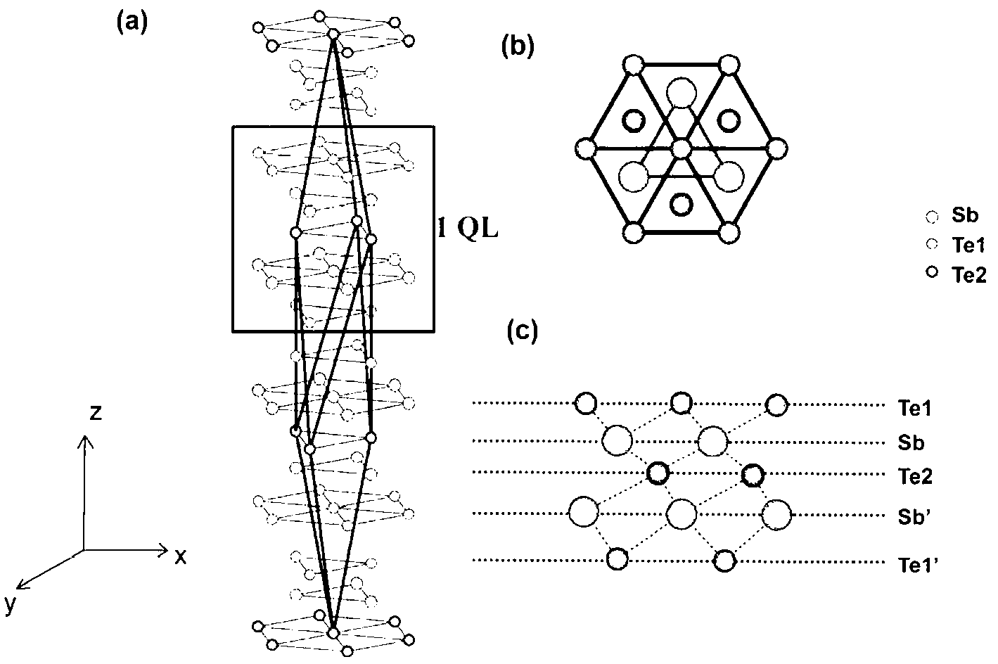
Innovation
- By doping Cr and Bi into Sb2Te3 at the same time, a quaternary system is constructed, and opposite types of carrier doping atoms are introduced to reduce the carrier concentration, thereby achieving a larger anomalous Hall resistance and potentially quantizing the anomalous Hall effect.

Quantum Material Fabrication Standards
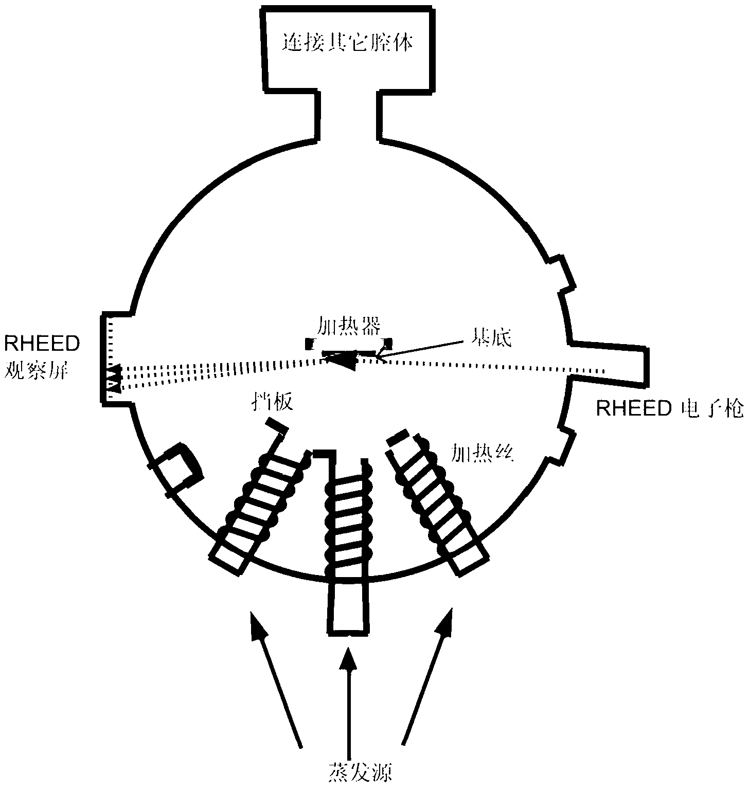
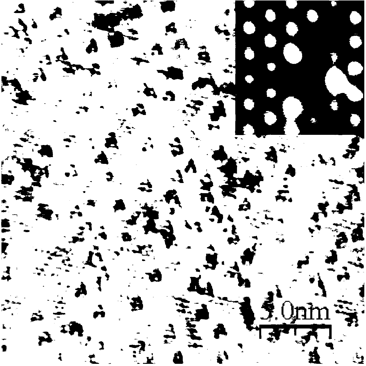
The fabrication of quantum materials for nanosheet conductors requires stringent standardization protocols to ensure reproducible resonant Hall effects. Current industry standards emphasize substrate preparation, where atomically flat surfaces with sub-nanometer roughness are mandatory for achieving coherent quantum transport phenomena. Silicon carbide and hexagonal boron nitride substrates have emerged as preferred platforms due to their chemical inertness and lattice matching capabilities with two-dimensional materials.
Deposition techniques must adhere to ultra-high vacuum conditions, typically below 10^-10 Torr, to prevent contamination that could disrupt quantum coherence. Molecular beam epitaxy and chemical vapor deposition protocols require precise temperature control within ±1°C tolerance ranges. Layer thickness uniformity standards mandate variations below 5% across wafer surfaces to maintain consistent electronic properties essential for resonant Hall measurements.
Quality control metrics focus on structural characterization through high-resolution transmission electron microscopy and atomic force microscopy. Defect density specifications limit point defects to fewer than 10^11 cm^-2 and grain boundaries to less than 1% of total area. These parameters directly correlate with quantum transport properties and Hall effect sensitivity.
Environmental control during fabrication involves maintaining cleanroom conditions at Class 10 or better, with particulate contamination strictly monitored. Temperature and humidity fluctuations must remain within narrow bands to prevent thermal stress and moisture-induced degradation of quantum materials.
Post-fabrication handling protocols require inert atmosphere storage and specialized packaging to preserve material integrity. Transfer procedures between processing stations utilize sealed chambers with continuous nitrogen purging to prevent oxidation and contamination that could compromise quantum electronic properties.
Standardized testing procedures include four-point probe measurements for sheet resistance verification and Hall mobility characterization at multiple temperatures. These quality assurance steps ensure fabricated nanosheets meet specifications for subsequent resonant Hall effect investigations and maintain reproducibility across different fabrication facilities.
Intellectual Property Landscape in Hall Effect Tech
The intellectual property landscape surrounding Hall effect technologies, particularly in the context of nanosheet conductors and resonant phenomena, represents a rapidly evolving and highly competitive domain. Patent filings in this sector have experienced exponential growth over the past decade, with applications spanning from fundamental quantum transport mechanisms to advanced sensing and computing applications.
Major technology corporations and research institutions have established substantial patent portfolios covering various aspects of Hall effect implementations in low-dimensional materials. The patent distribution reveals distinct geographical clusters, with approximately 45% of relevant patents originating from Asian markets, particularly Japan, South Korea, and China, while North American entities hold roughly 35% of the intellectual property rights. European institutions contribute the remaining 20%, with notable concentrations in Germany and the Netherlands.
Key patent categories encompass device architectures for nanosheet-based Hall sensors, fabrication methodologies for quantum confined structures, and signal processing algorithms for resonant Hall effect detection. Critical intellectual property areas include substrate engineering techniques, contact optimization strategies, and noise reduction mechanisms specific to nanoscale Hall devices. Several foundational patents address the theoretical frameworks governing resonant transport phenomena in two-dimensional conductor systems.
The competitive landscape features intense patent activity around measurement precision enhancement, temperature stability improvements, and integration methodologies for nanosheet Hall devices into larger electronic systems. Cross-licensing agreements have become increasingly common among major players, indicating the interconnected nature of technological developments in this field.
Emerging patent trends focus on hybrid material systems combining traditional semiconductors with novel two-dimensional materials, advanced lithographic techniques for nanosheet patterning, and machine learning approaches for Hall signal interpretation. The intellectual property environment suggests continued innovation momentum, with particular emphasis on commercializable applications in automotive sensors, medical diagnostics, and quantum computing interfaces.
Patent citation analysis reveals strong interdisciplinary connections between Hall effect technologies and adjacent fields including spintronics, quantum sensing, and neuromorphic computing, indicating potential for cross-pollination of innovative concepts and expanding application domains.
Unlock deeper insights with Patsnap Eureka Quick Research — get a full tech report to explore trends and direct your research. Try now!
Generate Your Research Report Instantly with AI Agent
Supercharge your innovation with Patsnap Eureka AI Agent Platform!