

Chip Embedding for Energy Storage Systems: Maximizing Power Density
MAY 29, 20269 MIN READ
Generate Your Research Report Instantly with AI Agent
Patsnap Eureka helps you evaluate technical feasibility & market potential.
Chip Embedding Energy Storage Background and Objectives
The evolution of electronic systems has consistently driven the demand for higher power density solutions, particularly in energy storage applications. Traditional energy storage architectures face significant challenges in meeting the compact form factor requirements of modern electronic devices while maintaining optimal performance characteristics. The spatial constraints imposed by conventional battery packaging and discrete component arrangements have created bottlenecks in achieving maximum energy efficiency per unit volume.
Chip embedding technology represents a paradigm shift in energy storage system design, where energy storage components are directly integrated into semiconductor substrates or package structures. This approach fundamentally alters the traditional separation between active electronic components and energy storage elements, enabling unprecedented levels of miniaturization and performance optimization. The technology leverages advanced semiconductor manufacturing processes to create hybrid structures that combine computational and energy storage capabilities within unified platforms.
The historical development of energy storage systems has progressed from bulky external batteries to increasingly sophisticated integrated solutions. Early implementations focused primarily on discrete component optimization, while recent advances have emphasized system-level integration approaches. The emergence of Internet of Things devices, wearable electronics, and autonomous systems has accelerated the need for ultra-compact energy storage solutions that can operate reliably in space-constrained environments.
Current market drivers include the proliferation of edge computing devices, medical implants, and portable consumer electronics that demand extended operational lifetimes without compromising device miniaturization. The automotive industry's transition toward electrification and the growing deployment of wireless sensor networks further amplify the importance of high-power-density energy storage solutions.
The primary objective of chip embedding for energy storage systems centers on maximizing power density through innovative integration methodologies. This involves developing manufacturing processes that enable seamless incorporation of energy storage materials into semiconductor substrates while maintaining electrical performance and thermal management capabilities. Key technical goals include achieving power densities exceeding conventional solutions by factors of three to five, establishing reliable interconnection schemes between embedded storage elements and active circuits, and ensuring long-term operational stability under various environmental conditions.
Secondary objectives encompass cost reduction through manufacturing process consolidation, improved system reliability through reduced interconnection complexity, and enhanced design flexibility enabling application-specific optimization. The ultimate vision involves creating self-powered electronic systems that eliminate external battery dependencies while providing sufficient energy capacity for extended autonomous operation.
Market Demand for High Power Density Energy Systems
The global energy storage market is experiencing unprecedented growth driven by the urgent need for higher power density solutions across multiple sectors. Electric vehicle manufacturers are pushing the boundaries of battery technology to achieve faster charging times and extended range capabilities, creating substantial demand for energy storage systems that can deliver maximum power output within minimal physical footprints. The automotive sector alone represents a significant portion of this demand, with manufacturers seeking solutions that can reduce vehicle weight while maintaining or improving performance metrics.
Data centers and cloud computing infrastructure represent another critical demand driver for high power density energy storage systems. As digital transformation accelerates globally, these facilities require backup power solutions that can deliver substantial energy output while occupying minimal rack space. The increasing adoption of edge computing and 5G networks further amplifies this need, as distributed infrastructure requires compact yet powerful energy storage solutions at numerous deployment points.
Consumer electronics continue to evolve toward thinner, lighter designs while demanding greater functionality and longer battery life. Smartphones, tablets, wearable devices, and portable computing equipment all require energy storage solutions that maximize power delivery within increasingly constrained form factors. The proliferation of Internet of Things devices and smart home technologies creates additional market segments where space-efficient, high-performance energy storage is essential.
Industrial applications present substantial opportunities for chip-embedded energy storage systems, particularly in robotics, automation equipment, and portable industrial tools. Manufacturing facilities increasingly rely on automated systems that require reliable, high-density power sources to maintain operational efficiency. The growing emphasis on industrial digitization and smart manufacturing processes creates sustained demand for compact energy storage solutions that can support advanced sensor networks and control systems.
Renewable energy integration challenges are driving demand for grid-scale energy storage systems that can rapidly respond to fluctuating power generation from solar and wind sources. Utility companies and energy providers require storage solutions that can deliver high power output during peak demand periods while maintaining compact installations that minimize land use requirements.
The aerospace and defense sectors represent specialized but lucrative market segments where power density requirements are particularly stringent. Unmanned aerial vehicles, satellite systems, and portable military equipment all demand energy storage solutions that maximize power output while minimizing weight and volume constraints. These applications often justify premium pricing for advanced energy storage technologies that deliver superior performance characteristics.
Current State and Challenges of Chip-Embedded Storage
The current landscape of chip-embedded energy storage systems represents a convergence of semiconductor technology and energy storage solutions, driven by the increasing demand for compact, high-performance power systems in portable electronics, electric vehicles, and IoT devices. This emerging field focuses on integrating energy storage components directly onto semiconductor substrates or within chip packages, fundamentally challenging traditional approaches to power delivery and energy management.
Existing chip-embedded storage technologies primarily encompass on-chip supercapacitors, thin-film batteries, and micro-scale electrochemical capacitors. These solutions leverage advanced microfabrication techniques including photolithography, chemical vapor deposition, and atomic layer deposition to create energy storage structures at the microscale. Current implementations achieve energy densities ranging from 1-10 mWh/cm² for thin-film batteries and power densities of 10-100 mW/cm² for on-chip supercapacitors.
The primary technical challenges center around maximizing power density while maintaining reliability and manufacturability. Material limitations pose significant constraints, as traditional battery chemistries struggle to maintain performance when scaled to microscopic dimensions. The limited thickness of deposited films restricts energy capacity, while the high surface-to-volume ratio at microscales introduces parasitic effects that reduce overall efficiency.
Thermal management emerges as a critical challenge, as the proximity of energy storage elements to active semiconductor components creates complex heat dissipation requirements. The mismatch in thermal expansion coefficients between storage materials and silicon substrates leads to mechanical stress issues that can compromise device reliability over extended cycling periods.
Manufacturing scalability represents another substantial hurdle, as current fabrication processes for chip-embedded storage require specialized equipment and materials that significantly increase production costs. The integration of electrochemical processes with standard CMOS fabrication flows introduces contamination risks and process compatibility issues that limit widespread adoption.
Interface engineering between the storage elements and the host semiconductor presents ongoing challenges in terms of electrical connectivity, mechanical adhesion, and electrochemical stability. The development of suitable electrolyte systems that remain stable in the semiconductor processing environment while providing adequate ionic conductivity continues to be a major research focus.
Despite these challenges, recent advances in nanostructured electrodes, solid-state electrolytes, and 3D integration techniques are beginning to address some fundamental limitations, paving the way for more practical implementations of chip-embedded energy storage systems with enhanced power density characteristics.
Existing Chip Embedding Solutions for Power Density
01 Thermal management and heat dissipation techniques for high-density chip embedding
Advanced thermal management solutions are essential for managing heat generated in high-density chip embedding applications. These techniques include specialized heat sinks, thermal interface materials, and cooling structures that efficiently dissipate heat from embedded chips. The methods focus on maintaining optimal operating temperatures while maximizing power density through improved thermal conductivity and heat transfer mechanisms.- Thermal management and heat dissipation techniques for high-density chip embedding: Advanced thermal management solutions are essential for managing heat generation in high power density embedded chips. These techniques include specialized heat sinks, thermal interface materials, and cooling structures that efficiently dissipate heat from densely packed semiconductor devices. The methods focus on maintaining optimal operating temperatures while maximizing power output per unit area.
- Power delivery and distribution architectures for embedded chip systems: Efficient power delivery networks are crucial for supporting high power density in embedded chip applications. These architectures involve optimized power distribution schemes, voltage regulation modules, and power management integrated circuits that ensure stable power supply to densely packed components while minimizing power losses and electromagnetic interference.
- Advanced packaging technologies for high-density chip integration: Innovative packaging solutions enable higher chip embedding densities through three-dimensional stacking, system-in-package configurations, and multi-chip modules. These technologies utilize advanced interconnection methods, substrate materials, and assembly processes to achieve compact form factors while maintaining electrical performance and reliability in high power density applications.
- Substrate and interconnect design for power-dense embedded systems: Specialized substrate materials and interconnect structures are designed to handle high current densities and power loads in embedded chip applications. These designs incorporate low-resistance pathways, optimized via structures, and advanced materials that support efficient power transmission while minimizing signal integrity issues and thermal hotspots.
- System-level optimization and control methods for power density management: Comprehensive system-level approaches optimize power density through intelligent control algorithms, dynamic power scaling, and adaptive management techniques. These methods monitor and adjust operating parameters in real-time to maximize power efficiency while preventing thermal runaway and ensuring system reliability in high-density embedded chip configurations.
02 Power delivery and distribution systems for embedded chips
Efficient power delivery systems are crucial for supporting high power density in chip embedding applications. These systems incorporate advanced power distribution networks, voltage regulation modules, and power management circuits that ensure stable and efficient power supply to embedded components. The designs optimize power conversion efficiency while minimizing power losses and electromagnetic interference.Expand Specific Solutions03 Packaging and interconnect technologies for high-density integration
Specialized packaging technologies enable higher power density through improved chip embedding techniques. These approaches include advanced substrate materials, multi-layer interconnect structures, and innovative bonding methods that allow for closer chip placement and better electrical performance. The technologies focus on reducing parasitic effects while increasing integration density.Expand Specific Solutions04 Power monitoring and control systems for embedded applications
Sophisticated monitoring and control systems are implemented to manage power consumption and optimize performance in high-density chip embedding scenarios. These systems include real-time power measurement circuits, adaptive power scaling mechanisms, and intelligent control algorithms that dynamically adjust operating parameters based on thermal and electrical conditions.Expand Specific Solutions05 Substrate and material innovations for enhanced power density
Novel substrate materials and structural innovations enable higher power density in chip embedding applications. These developments include advanced dielectric materials, improved conductor geometries, and specialized substrate designs that provide better electrical and thermal properties. The innovations focus on reducing size while maintaining or improving performance characteristics.Expand Specific Solutions
Key Players in Chip-Embedded Energy Storage Industry
The chip embedding technology for energy storage systems represents an emerging sector within the broader energy storage market, which is experiencing rapid growth driven by electrification trends and renewable energy integration. The industry is transitioning from early development to commercialization phase, with market size expanding significantly as automotive and grid-scale applications accelerate adoption. Technology maturity varies considerably across key players, with established semiconductor companies like Samsung Electronics, Taiwan Semiconductor Manufacturing, and Infineon Technologies providing foundational chip manufacturing capabilities, while energy specialists such as Huawei Digital Power Technologies and IHI Terrasun Solutions focus on system integration. Traditional automotive manufacturers like Toyota Motor and Audi AG are driving demand through electric vehicle development, supported by research institutions including Northwestern University and Georgia Tech Research Corp. advancing fundamental technologies. The competitive landscape shows convergence between semiconductor expertise and energy storage applications, indicating moderate technology maturity with significant growth potential.
Infineon Technologies AG
Technical Solution: Infineon has developed advanced power semiconductor solutions specifically designed for energy storage systems, focusing on silicon carbide (SiC) and gallium nitride (GaN) technologies that enable higher power density through reduced switching losses and improved thermal management. Their chip embedding approach integrates power management ICs directly into battery management systems, achieving up to 98% efficiency in power conversion while reducing system volume by 30%. The company's CoolSiC MOSFETs and OptiMOS power transistors are optimized for fast switching frequencies up to 100kHz, enabling smaller passive components and higher power density in energy storage applications.
Strengths: Industry-leading power semiconductor expertise, proven SiC and GaN technologies, strong automotive and industrial market presence. Weaknesses: Higher cost compared to silicon-based solutions, complex manufacturing processes requiring specialized facilities.
Taiwan Semiconductor Manufacturing Co., Ltd.
Technical Solution: TSMC provides advanced foundry services for power management and energy storage control chips, enabling customers to develop highly integrated solutions using their 16nm FinFET and specialized power management process technologies. Their chip embedding approach focuses on manufacturing ultra-low power consumption control chips that can be directly integrated into battery management systems, achieving power conversion efficiencies above 95% while reducing board space requirements by 40%. TSMC's advanced packaging technologies, including InFO and CoWoS, enable 3D integration of power management functions with sensing and communication capabilities in compact form factors.
Strengths: Leading-edge semiconductor manufacturing processes, advanced packaging capabilities, strong ecosystem of design partners. Weaknesses: Pure foundry model limits direct system integration expertise, dependency on customer designs for energy storage applications.
Core Technologies in Chip-Based Energy Storage
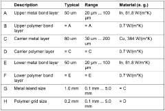
Embedded power package
PatentWO2025123276A1
Innovation
- The solution involves increasing the Cu line thickness in selected areas of the power module using metal layer reinforcement, allowing for enhanced current carrying capability and thermal mass without affecting areas requiring high density.


Hybrid bond sheet and cooled semiconductor power module
PatentWO2023179090A1
Innovation
- Direct vertical connections between pre-manufactured PCB core layers without outer layer plating process, enabling 3D stacking in chip embedding technology for power electronics applications.
- Large connection metal areas embedded in isolation material within the projected physical outline of embedded components, achieving high current carrying capability and thermal conductivity simultaneously.
- Formation of reliable vertical connections through diffusion soldering or sintering with intermetallic phases that do not remelt at bond temperature, suitable for high-power applications.
Safety Standards for Chip-Embedded Energy Systems
The safety standards for chip-embedded energy systems represent a critical framework governing the integration of semiconductor components within energy storage architectures. Current regulatory landscapes encompass multiple international standards including IEC 62133 for portable sealed secondary cells, UL 2054 for household and commercial batteries, and emerging IEEE standards specifically addressing embedded electronic components in energy systems. These standards establish fundamental safety requirements covering thermal management, electrical isolation, mechanical integrity, and electromagnetic compatibility.
Thermal safety protocols constitute the primary concern for chip-embedded systems, given the concentrated heat generation from both energy storage processes and semiconductor operations. Standards mandate specific temperature monitoring requirements, thermal runaway prevention mechanisms, and heat dissipation pathways. The integration of chips within energy cells necessitates enhanced thermal modeling and real-time temperature sensing capabilities to prevent catastrophic failures that could compromise both the embedded electronics and the energy storage medium.
Electrical safety standards address isolation requirements between high-voltage energy storage components and low-voltage embedded chips. These specifications define minimum creepage distances, clearance requirements, and insulation coordination principles. Protection against overvoltage, undervoltage, and transient electrical events must be implemented through both hardware design and embedded software algorithms. The standards also establish requirements for fail-safe modes and emergency shutdown procedures.
Mechanical safety considerations encompass structural integrity under various stress conditions including vibration, shock, and pressure variations. Standards specify testing protocols for mechanical durability, particularly focusing on the interfaces between embedded chips and energy storage materials. Special attention is given to preventing mechanical damage that could lead to internal short circuits or compromise the protective barriers between different system components.
Certification processes for chip-embedded energy systems require comprehensive testing protocols that validate compliance with multiple safety domains simultaneously. These processes involve accelerated aging tests, fault injection scenarios, and environmental stress screening. The certification framework also addresses cybersecurity aspects, establishing requirements for secure communication protocols and protection against malicious attacks that could compromise system safety through the embedded chip interfaces.
Thermal Management in High-Density Chip Storage
Thermal management represents one of the most critical challenges in high-density chip storage systems for energy applications. As chip embedding technology advances toward maximizing power density, the concentration of electronic components generates substantial heat loads that can severely impact system performance, reliability, and safety. The thermal challenge becomes exponentially more complex when multiple chips are densely packed within confined storage enclosures.
The primary thermal concern stems from the inherent heat generation characteristics of embedded chips during charge-discharge cycles. High-performance energy storage chips typically operate at elevated power levels, producing heat fluxes that can exceed 100 W/cm² in advanced configurations. This heat generation creates localized hot spots that can trigger thermal runaway conditions, particularly in lithium-based storage systems, leading to catastrophic failures and safety hazards.
Traditional air cooling methods prove inadequate for high-density chip storage applications due to limited heat transfer coefficients and space constraints. The compact nature of embedded chip systems restricts airflow pathways, creating thermal bottlenecks that compromise overall system efficiency. Additionally, temperature gradients across chip arrays can cause uneven aging and performance degradation, reducing the operational lifespan of storage systems.
Advanced thermal management solutions focus on multi-modal heat dissipation strategies. Liquid cooling systems utilizing micro-channel heat exchangers offer superior thermal conductivity, enabling efficient heat removal from densely packed chip configurations. Phase-change materials integrated within chip packaging provide passive thermal regulation by absorbing excess heat during peak operations and releasing it during low-power periods.
Thermal interface materials play a crucial role in optimizing heat transfer between chips and cooling systems. High-conductivity materials such as graphene-enhanced thermal pads and liquid metal interfaces significantly reduce thermal resistance, improving overall heat dissipation efficiency. These materials must maintain stable performance across wide temperature ranges while ensuring electrical isolation between components.
System-level thermal design requires sophisticated modeling and simulation tools to predict temperature distributions and optimize cooling strategies. Computational fluid dynamics analysis helps identify optimal chip placement patterns and cooling channel configurations that minimize thermal hotspots while maintaining compact form factors essential for high-density storage applications.
Unlock deeper insights with Patsnap Eureka Quick Research — get a full tech report to explore trends and direct your research. Try now!
Generate Your Research Report Instantly with AI Agent
Supercharge your innovation with Patsnap Eureka AI Agent Platform!