

Optimizing Cost Efficiency in Chip Embedding for Low-Volume Prototyping
MAY 29, 20269 MIN READ
Generate Your Research Report Instantly with AI Agent
Patsnap Eureka helps you evaluate technical feasibility & market potential.
Chip Embedding Cost Challenges and Goals
Chip embedding technology has evolved significantly over the past two decades, transitioning from traditional through-hole mounting to advanced surface-mount and embedded packaging solutions. The historical development began with basic component integration methods in the 1990s, progressing through flip-chip bonding innovations in the early 2000s, and culminating in today's sophisticated system-in-package and wafer-level packaging technologies. This evolution has been driven by the relentless pursuit of miniaturization, performance enhancement, and cost optimization across various electronic applications.
The current technological landscape presents a fundamental challenge in balancing cost efficiency with performance requirements, particularly in low-volume prototyping scenarios. Unlike high-volume manufacturing where economies of scale naturally reduce per-unit costs, prototype development faces inherent cost penalties due to limited production quantities, specialized tooling requirements, and the need for flexible manufacturing processes. This creates a complex optimization problem where traditional cost-reduction strategies become less effective.
The primary technical objectives center on developing cost-effective embedding methodologies that maintain acceptable performance standards while accommodating the unique constraints of prototype environments. Key goals include minimizing setup costs through standardized processes, reducing material waste through optimized design approaches, and implementing scalable solutions that can transition smoothly from prototype to production phases. Additionally, the technology aims to achieve reliable electrical and thermal performance while maintaining mechanical integrity under various operating conditions.
Contemporary challenges encompass multiple dimensions including material selection optimization, process parameter standardization, and quality assurance protocols. The integration of advanced materials such as low-loss dielectrics and high-thermal-conductivity substrates introduces additional cost variables that must be carefully managed. Furthermore, the need for rapid prototyping cycles demands flexible manufacturing approaches that can accommodate design iterations without significant cost penalties.
The strategic vision for chip embedding cost optimization involves establishing a comprehensive framework that addresses both immediate prototyping needs and long-term scalability requirements. This includes developing modular design approaches, implementing cost-predictive modeling tools, and creating standardized process libraries that can be efficiently deployed across different project requirements while maintaining the flexibility essential for innovative prototype development.
Market Demand for Low-Volume Prototype Solutions
The market demand for low-volume prototype solutions has experienced significant growth across multiple industries, driven by the accelerating pace of product development cycles and the increasing complexity of electronic systems. Startups, research institutions, and established companies developing innovative products require flexible manufacturing approaches that can accommodate small batch sizes without the prohibitive costs traditionally associated with semiconductor fabrication and assembly processes.
The consumer electronics sector represents a substantial portion of this demand, particularly among companies developing Internet of Things devices, wearable technology, and smart home products. These organizations typically require prototype quantities ranging from dozens to several hundred units during various development phases, making traditional high-volume manufacturing economically unfeasible. The automotive industry has also emerged as a key driver, especially with the rise of electric vehicles and autonomous driving technologies requiring extensive prototyping of electronic control units and sensor systems.
Medical device manufacturers constitute another critical market segment, where regulatory requirements necessitate extensive prototype testing before commercial production. The stringent validation processes in healthcare applications create sustained demand for cost-effective low-volume solutions that can support iterative design improvements without significant financial barriers.
The aerospace and defense sectors have historically relied on low-volume production due to the specialized nature of their applications. However, recent trends toward miniaturization and increased electronic content in these systems have intensified the need for optimized chip embedding solutions that can deliver reliability while managing costs effectively.
Market dynamics indicate a growing preference for rapid prototyping capabilities that can bridge the gap between proof-of-concept and pilot production. Companies increasingly seek solutions that offer scalability, allowing them to transition from prototype quantities to small-scale production without requiring complete process redesigns. This trend has created opportunities for specialized service providers and equipment manufacturers to develop targeted solutions for the low-volume segment.
The geographic distribution of demand shows concentration in technology hubs across North America, Europe, and Asia-Pacific regions, with emerging markets beginning to contribute as local innovation ecosystems mature and expand their electronic product development capabilities.
Current State and Cost Barriers in Chip Embedding
Chip embedding technology for low-volume prototyping currently faces significant economic challenges that limit its accessibility to smaller enterprises and research institutions. The traditional semiconductor packaging industry has been optimized for high-volume production runs, typically requiring minimum order quantities of thousands to tens of thousands of units to achieve cost-effective pricing. This volume-centric model creates substantial barriers for prototype development, where quantities often range from single units to hundreds of pieces.
The current cost structure in chip embedding is dominated by several key factors. Initial setup costs for embedding processes can range from $5,000 to $50,000 depending on the complexity of the substrate design and the number of embedded components. These costs include tooling preparation, substrate fabrication setup, and process qualification procedures. For low-volume runs, these fixed costs translate to prohibitively high per-unit expenses, often exceeding $100-500 per prototype unit compared to $1-10 for high-volume production.
Material costs present another significant barrier, as specialized embedding substrates and advanced packaging materials are typically sold in bulk quantities with minimum purchase requirements. Standard substrate materials for chip embedding, such as modified epoxy resins and glass-fiber composites, often require minimum orders of several square meters, far exceeding prototype needs. This results in material utilization rates below 10% for typical prototype projects, dramatically inflating effective material costs.
Manufacturing infrastructure represents a critical bottleneck in the current landscape. Most chip embedding facilities are designed for continuous, high-throughput operations using automated placement and lamination systems. These systems require extensive setup time and calibration procedures that can take 8-24 hours, making them economically unviable for small batch production. The lack of flexible, small-scale embedding equipment specifically designed for prototype volumes creates a significant gap in the market.
Quality assurance and testing protocols further compound cost challenges. Current industry standards require comprehensive electrical testing, thermal cycling, and reliability assessments that can add $50-200 per prototype unit. While these procedures are essential for production validation, their application to early-stage prototypes often represents an disproportionate cost burden relative to the prototype's developmental value.
The geographic concentration of advanced chip embedding capabilities in specific regions also contributes to cost barriers. Limited local access to embedding services forces many organizations to rely on distant suppliers, adding shipping costs, extended lead times, and communication complexities that can increase total project costs by 20-40%.
Existing Cost Optimization Solutions for Chip Embedding
01 Advanced chip packaging and embedding techniques
Various advanced packaging methods and embedding techniques are employed to reduce manufacturing costs while maintaining chip performance. These techniques focus on optimizing the physical integration of chips into substrates and improving the overall packaging efficiency through innovative structural designs and material selection.- Advanced chip packaging and embedding techniques: Various advanced packaging methods and embedding techniques are employed to reduce manufacturing costs while maintaining chip performance. These techniques include optimized substrate materials, improved bonding processes, and innovative encapsulation methods that streamline production workflows and reduce material waste.
- Cost-effective substrate and interconnection solutions: Development of economical substrate materials and interconnection architectures that maintain electrical performance while reducing overall production costs. These solutions focus on simplified manufacturing processes, reduced layer counts, and alternative materials that provide comparable functionality at lower expense.
- Automated manufacturing and assembly processes: Implementation of automated systems and robotics in chip embedding processes to reduce labor costs and improve production efficiency. These systems incorporate precision placement equipment, automated inspection capabilities, and streamlined workflow management to minimize human intervention and associated costs.
- Multi-chip integration and system-in-package solutions: Strategies for integrating multiple chips within single packages to achieve cost efficiencies through shared resources and reduced individual packaging requirements. These approaches optimize space utilization, reduce interconnection complexity, and enable economies of scale in manufacturing processes.
- Quality control and yield optimization methods: Implementation of advanced testing and quality assurance techniques to maximize production yields and minimize defect-related costs. These methods include real-time monitoring systems, predictive maintenance protocols, and statistical process control measures that identify and prevent costly manufacturing errors.
02 Cost-effective manufacturing processes and automation
Implementation of automated manufacturing processes and streamlined production workflows significantly reduces labor costs and improves yield rates. These approaches include optimized assembly line configurations, automated testing procedures, and quality control systems that minimize waste and rework during chip embedding operations.Expand Specific Solutions03 Material optimization and substrate design
Strategic selection and optimization of substrate materials and interconnect designs help reduce overall production costs while ensuring reliable chip performance. This includes the use of cost-effective materials, improved thermal management solutions, and enhanced electrical connectivity designs that balance performance requirements with economic considerations.Expand Specific Solutions04 Multi-chip integration and space utilization
Efficient utilization of available space through multi-chip integration techniques and compact design methodologies reduces per-unit costs by maximizing functionality within minimal footprint. These approaches include stacked configurations, shared interconnects, and optimized layout designs that improve cost efficiency through better space utilization.Expand Specific Solutions05 Testing and quality assurance optimization
Streamlined testing procedures and quality assurance methodologies reduce overall production costs by minimizing testing time and improving defect detection efficiency. These systems incorporate automated testing protocols, statistical quality control methods, and predictive maintenance approaches that ensure product reliability while reducing operational expenses.Expand Specific Solutions
Key Players in Prototype and Chip Embedding Industry
The chip embedding market for low-volume prototyping is experiencing rapid evolution driven by increasing demand for customized semiconductor solutions across automotive, IoT, and consumer electronics sectors. The industry is transitioning from mature to growth stage, with market size expanding significantly as companies seek cost-effective prototyping alternatives. Technology maturity varies considerably across market players, with established leaders like Taiwan Semiconductor Manufacturing Co., Intel Corp., and Samsung demonstrating advanced capabilities in specialized foundry services and embedded processing solutions. Mid-tier players including GlobalFoundries, Tower Semiconductor, and Infineon Technologies are developing competitive cost-optimization strategies, while emerging companies like eMemory Technology and Etron Technology focus on niche applications. Chinese manufacturers such as SMIC and Shanghai Huahong Grace are rapidly advancing their technological capabilities, intensifying global competition and driving innovation in cost-efficient embedding solutions for prototype development.
Texas Instruments Incorporated
Technical Solution: Texas Instruments focuses on cost-efficient prototyping solutions through their extensive analog and mixed-signal process technologies, offering specialized services for embedded applications. Their prototyping approach emphasizes proven, mature process nodes that provide excellent cost-performance characteristics for low-volume production. TI maintains flexible manufacturing capabilities that can accommodate small batch sizes while leveraging their advanced packaging technologies including chip-scale packages and system-in-package solutions. The company provides comprehensive design support and reference designs that accelerate prototype development cycles, reducing overall time-to-market and development costs for embedded chip applications.
Strengths: Extensive analog/mixed-signal expertise, mature and cost-effective process technologies, comprehensive design support ecosystem. Weaknesses: Limited digital processing capabilities, focus primarily on analog and power management applications.
Taiwan Semiconductor Manufacturing Co., Ltd.
Technical Solution: TSMC offers comprehensive prototyping services through their Open Innovation Platform (OIP), providing access to advanced process nodes including 7nm and 5nm technologies for low-volume production. Their shuttle services allow multiple designs to share mask costs, significantly reducing NRE expenses for prototyping. The company provides flexible packaging solutions and maintains dedicated prototype fabrication lines that can handle small batch orders efficiently. TSMC's advanced process control and yield optimization techniques ensure high-quality results even for limited production runs, making it cost-effective for companies developing proof-of-concept designs.
Strengths: Industry-leading process technology, established shuttle programs for cost sharing, comprehensive design ecosystem support. Weaknesses: Higher minimum order quantities compared to specialty prototype foundries, longer lead times due to high demand.
Core Innovations in Low-Volume Embedding Processes
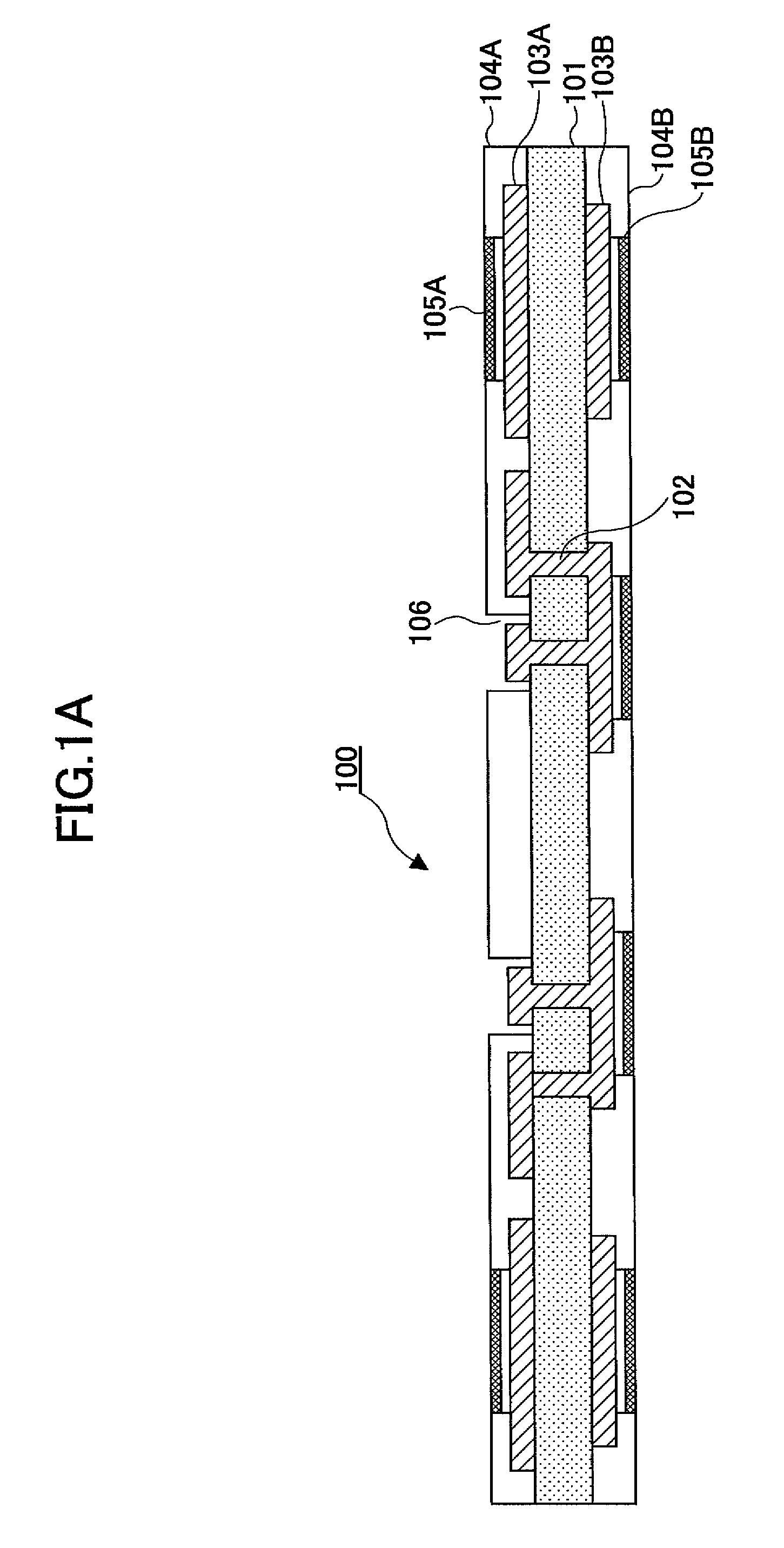
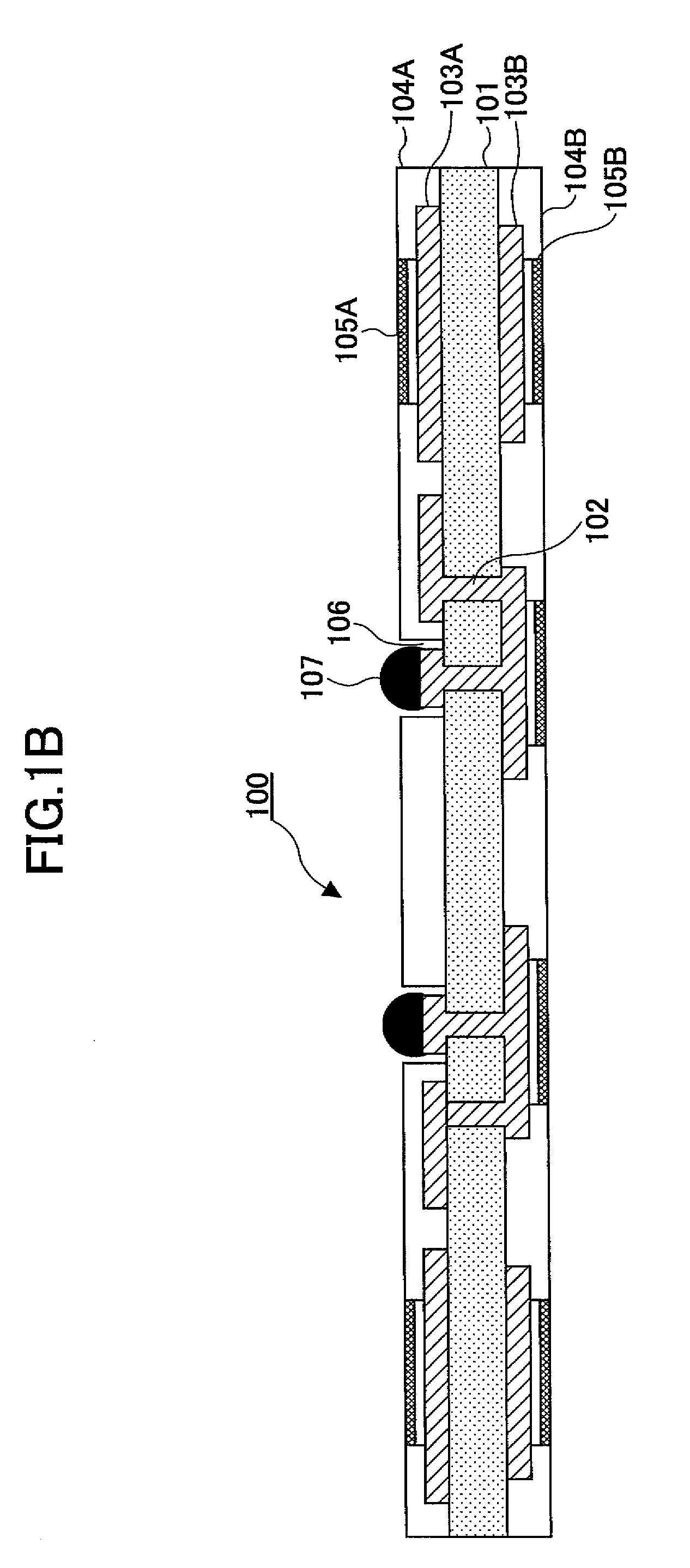
Low cost integrated circuit bonding process
PatentInactiveUS4661192A
Innovation
- A process involving the formation of conductive balls on bonding pads using a readily available wire bonder, followed by planarization and coating with conductive epoxy, allowing for bonding to a die support frame without the need for expensive bumping, utilizing existing wire bonding equipment.


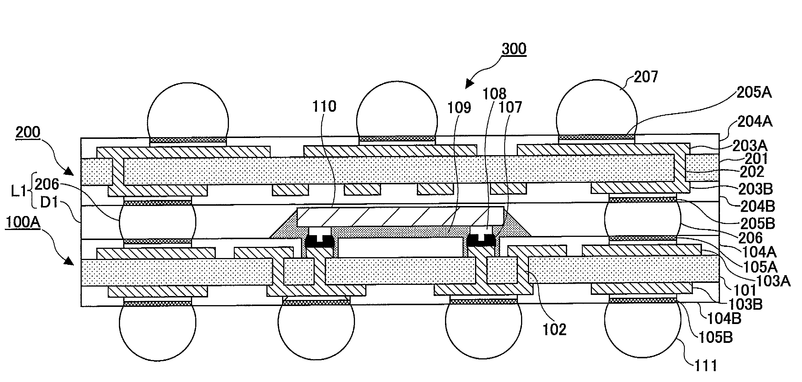
Chip embedded substrate and method of producing the same
PatentActiveUS7989707B2
Innovation
- A method involving the stacking of substrates with formed wirings, where a semiconductor chip is encapsulated between two substrates, and electrical connections are made between the wirings of these substrates to form multilayered connections, enhancing reliability and yield.

Supply Chain Optimization for Small-Batch Production
Supply chain optimization for small-batch production in chip embedding presents unique challenges that differ significantly from high-volume manufacturing paradigms. Traditional semiconductor supply chains are designed for economies of scale, where unit costs decrease dramatically with volume increases. However, low-volume prototyping requires a fundamentally different approach that prioritizes flexibility, speed, and cost-per-unit optimization rather than total volume efficiency.
The primary challenge lies in minimum order quantities imposed by component suppliers and fabrication facilities. Most semiconductor manufacturers establish MOQs that can range from thousands to millions of units, making direct procurement prohibitively expensive for prototype quantities. This creates a supply chain bottleneck where the cost of acquiring even basic components can exceed the entire prototype budget.
Inventory management becomes critical in small-batch scenarios. Unlike high-volume production where just-in-time delivery is feasible, prototype projects must balance carrying costs against stockout risks. Excess inventory ties up capital and may become obsolete before use, while insufficient stock can halt development timelines. Strategic partnerships with distributors who maintain diverse component inventories can mitigate these risks while providing access to smaller quantities at reasonable prices.
Alternative sourcing strategies have emerged to address these constraints. Component brokers and surplus dealers offer access to smaller quantities, though quality verification becomes paramount. Online marketplaces and peer-to-peer component exchanges provide additional sourcing options, particularly for legacy or hard-to-find components. However, these channels require robust authentication processes to ensure component authenticity and reliability.
Collaborative procurement models represent an innovative approach where multiple small-volume users aggregate their requirements to achieve better pricing and terms. Industry consortiums and shared fabrication services enable prototype developers to pool resources while maintaining individual project confidentiality. These models require sophisticated coordination mechanisms but can significantly reduce per-unit costs.
Supply chain digitization plays an increasingly important role in optimization. Real-time inventory tracking, predictive analytics for demand forecasting, and automated supplier qualification processes reduce administrative overhead while improving decision-making speed. Digital platforms that connect prototype developers with specialized suppliers create more efficient matching between supply and demand.
Risk mitigation strategies must account for the higher volatility inherent in small-batch supply chains. Dual sourcing, even at prototype scales, provides insurance against supplier disruptions. Flexible contracts that allow for quantity adjustments without significant penalties accommodate the uncertainty typical in prototype development phases.
Manufacturing Process Automation for Cost Reduction
Manufacturing process automation represents a critical pathway for achieving substantial cost reductions in chip embedding operations for low-volume prototyping environments. Traditional manual processes in prototype manufacturing often suffer from inconsistent quality, extended cycle times, and elevated labor costs that become particularly pronounced when dealing with precision chip embedding applications.
Automated pick-and-place systems have emerged as fundamental solutions for reducing labor-intensive assembly operations. These systems utilize computer vision and precision robotics to achieve consistent chip placement accuracy while minimizing material waste. Advanced placement machines can achieve positioning accuracies within ±25 micrometers, significantly reducing rework rates and associated costs. The integration of machine learning algorithms enables these systems to adapt to component variations and optimize placement strategies in real-time.
Automated optical inspection systems provide immediate quality feedback, eliminating the need for extensive manual inspection processes. These systems can detect placement errors, solder joint defects, and component orientation issues within seconds of assembly completion. Early defect detection prevents costly downstream failures and reduces the overall cost per prototype unit by minimizing scrap rates.
Process parameter optimization through automated control systems delivers consistent results across production batches. Automated reflow ovens with precise temperature profiling ensure optimal solder joint formation while reducing energy consumption. Smart conveyor systems with integrated sensors monitor component flow and automatically adjust processing speeds to maintain optimal throughput rates.
Data collection and analysis capabilities inherent in automated systems enable continuous process improvement. Real-time monitoring of key performance indicators such as cycle time, yield rates, and equipment utilization provides actionable insights for further cost optimization. Predictive maintenance algorithms reduce unexpected downtime and extend equipment lifecycle, distributing capital costs across larger production volumes.
Flexible automation solutions specifically designed for low-volume environments offer modular configurations that can be rapidly reconfigured for different chip embedding requirements. This adaptability reduces setup costs and enables efficient handling of diverse prototype specifications without requiring dedicated tooling for each variant.
Unlock deeper insights with Patsnap Eureka Quick Research — get a full tech report to explore trends and direct your research. Try now!
Generate Your Research Report Instantly with AI Agent
Supercharge your innovation with Patsnap Eureka AI Agent Platform!