

Chip Package vs PCB Warpage: Impact on Device Reliability
APR 7, 20269 MIN READ
Generate Your Research Report Instantly with AI Agent
PatSnap Eureka helps you evaluate technical feasibility & market potential.
Chip Package and PCB Warpage Background and Objectives
Warpage in semiconductor packaging and printed circuit boards represents one of the most critical reliability challenges in modern electronics manufacturing. This phenomenon occurs when thermal, mechanical, or chemical stresses cause deformation in materials, leading to non-planar surfaces that deviate from their original flat geometry. The increasing miniaturization of electronic devices, coupled with higher power densities and more complex multi-layer structures, has intensified the significance of warpage-related issues across the electronics industry.
The evolution of semiconductor packaging has witnessed a dramatic shift from traditional through-hole components to advanced surface-mount technologies, ball grid arrays, and system-in-package solutions. This progression has introduced new materials with varying coefficients of thermal expansion, creating interfaces where differential expansion and contraction occur during manufacturing processes and operational cycles. Similarly, PCB technology has advanced from simple single-layer boards to complex multi-layer structures incorporating high-density interconnects, embedded components, and advanced substrate materials.
Historical development in this field began with basic thermal cycling studies in the 1980s, progressing through finite element modeling capabilities in the 1990s, and evolving into today's sophisticated multi-physics simulation approaches. Early research focused primarily on solder joint reliability, but contemporary investigations encompass comprehensive system-level interactions between package warpage, board-level reliability, and overall device performance.
The primary technical objectives driving current research include developing predictive models that accurately forecast warpage behavior across various temperature profiles and mechanical loading conditions. Industry stakeholders seek to establish standardized measurement methodologies that enable consistent characterization of warpage phenomena across different manufacturing environments and product configurations.
Another critical objective involves optimizing material selection and structural design parameters to minimize warpage while maintaining electrical performance, thermal management, and cost-effectiveness. This includes investigating novel substrate materials, advanced underfill formulations, and innovative package architectures that inherently resist deformation under operational stresses.
Furthermore, the industry aims to develop real-time monitoring and control systems that can detect and compensate for warpage during manufacturing processes, particularly during reflow soldering and assembly operations where temperature-induced stresses are most pronounced.
Market Demand for Reliable Electronic Packaging Solutions
The global electronics industry faces mounting pressure to deliver increasingly reliable packaging solutions as devices become more compact, powerful, and mission-critical. Warpage-related failures in chip packages and PCBs represent a significant reliability concern that directly impacts product performance, manufacturing yields, and long-term durability. This challenge has created substantial market demand for advanced packaging technologies and solutions that can effectively mitigate warpage-induced stress and prevent device failures.
Consumer electronics manufacturers are driving significant demand for reliable packaging solutions as product lifecycles shorten and performance expectations rise. Smartphones, tablets, and wearable devices require packaging that can withstand thermal cycling, mechanical stress, and environmental conditions while maintaining electrical integrity. The automotive electronics sector presents particularly stringent reliability requirements, where packaging failures can have safety implications and costly warranty claims.
The data center and cloud computing infrastructure market represents another major demand driver for reliable electronic packaging. High-performance processors and memory modules generate substantial heat and operate under continuous stress, making warpage control critical for maintaining system reliability and preventing costly downtime. Enterprise customers increasingly prioritize packaging solutions that demonstrate proven reliability metrics and extended operational lifespans.
Industrial and aerospace applications create specialized demand for packaging solutions that can withstand extreme environmental conditions. These sectors require packaging technologies that maintain reliability across wide temperature ranges, high vibration environments, and extended operational periods. The growing adoption of Internet of Things devices in industrial settings further amplifies the need for robust packaging solutions that can operate reliably in harsh conditions.
The semiconductor packaging industry has responded to these market demands by developing advanced materials, design methodologies, and manufacturing processes specifically targeting warpage reduction. Demand for specialized substrates, underfill materials, and thermal interface materials continues to grow as manufacturers seek comprehensive solutions to address warpage-related reliability challenges.
Market growth in reliable electronic packaging is also driven by regulatory requirements and industry standards that mandate specific reliability performance criteria. Medical device manufacturers, telecommunications equipment providers, and defense contractors must comply with stringent reliability standards, creating consistent demand for proven packaging solutions that can meet these requirements while supporting ongoing technological advancement.
Current Warpage Issues and Reliability Challenges
Warpage-induced reliability challenges have become increasingly critical as electronic devices continue to miniaturize while demanding higher performance and functionality. The fundamental issue stems from the coefficient of thermal expansion (CTE) mismatch between different materials in the package-PCB assembly, creating mechanical stress during thermal cycling operations. This stress manifests as warpage deformation that can compromise solder joint integrity, leading to intermittent connections, complete joint failures, and ultimately device malfunction.
Current industry data indicates that warpage-related failures account for approximately 15-25% of all field reliability issues in consumer electronics, with the percentage rising significantly in high-performance computing applications. The problem is particularly acute in ball grid array (BGA) and chip scale package (CSP) configurations, where the large thermal mass differences between silicon die, organic substrates, and FR4 PCBs create substantial stress concentrations during reflow soldering and operational thermal cycles.
Package-level warpage typically occurs due to the interaction between the silicon die, die attach materials, substrate layers, and molding compounds. During reflow processes, temperatures reaching 260°C cause differential expansion rates that can generate warpage exceeding 100 micrometers in large packages. This deformation directly affects the coplanarity of solder balls, resulting in non-uniform joint formation and residual stress accumulation that degrades long-term reliability performance.
PCB warpage presents additional complexity as board-level thermal gradients during assembly create localized stress concentrations. Modern PCBs with multiple copper layers and varying trace densities exhibit non-uniform thermal expansion patterns, leading to twisted or saddle-shaped deformations. These deformations are further exacerbated by moisture absorption in organic materials, which can increase warpage by 30-50% under standard assembly conditions.
The reliability impact extends beyond initial assembly defects to include long-term degradation mechanisms. Thermal cycling during normal operation continuously stresses solder joints already compromised by initial warpage-induced misalignment. Finite element analysis studies demonstrate that even minor warpage of 50 micrometers can reduce solder joint fatigue life by up to 40%, while severe warpage conditions may cause immediate assembly failures or significantly shortened operational lifespans.
Emerging challenges include the adoption of lead-free soldering processes, which require higher reflow temperatures and create more severe warpage conditions. Additionally, the trend toward thinner package profiles and larger die sizes amplifies the warpage sensitivity, making traditional design approaches increasingly inadequate for next-generation electronic systems requiring enhanced reliability standards.
Existing Warpage Control and Measurement Solutions
01 Use of low-stress molding compounds and materials
Warpage in chip packages and PCBs can be reduced by selecting molding compounds and encapsulation materials with low coefficient of thermal expansion (CTE) and appropriate mechanical properties. These materials minimize thermal stress mismatch between different layers during manufacturing and operation. The selection of proper resin compositions and filler materials helps to balance the stress distribution and reduce deformation.- Use of low-stress molding compounds and materials: Warpage in chip packages and PCBs can be reduced by selecting molding compounds and encapsulation materials with lower coefficient of thermal expansion (CTE) and reduced internal stress. These materials minimize the mismatch between different layers during temperature cycling and reflow processes. Advanced epoxy molding compounds with fillers and modified resin systems can provide better stress distribution and dimensional stability, thereby reducing warpage deformation.
- Optimized package structure and substrate design: Structural modifications to the package and PCB design can effectively control warpage. This includes optimizing substrate thickness, adjusting copper layer distribution, implementing symmetrical layer stackup, and using stiffener rings or reinforcement structures. Balanced design of top and bottom layers helps to counteract bending moments caused by thermal expansion mismatch. Core thickness adjustment and material selection in multi-layer substrates also play crucial roles in warpage control.
- Die attach and adhesive layer optimization: The die attach process and adhesive materials significantly influence package warpage. Using die attach films or adhesives with appropriate elastic modulus and CTE can buffer the stress between the chip and substrate. Optimizing the thickness and curing conditions of the adhesive layer helps to minimize residual stress. Advanced underfill materials and their dispensing methods can also redistribute stress and reduce warpage during thermal cycling.
- Thermal management and process control: Controlling manufacturing process parameters is essential for warpage reduction. This includes optimizing reflow profiles, curing temperatures, and cooling rates to minimize thermal stress accumulation. Implementing step-by-step temperature ramping and controlled cooling can reduce warpage. Pre-heating and post-mold curing processes should be carefully designed to relieve internal stress. Process monitoring and real-time adjustment based on warpage measurement feedback can further improve manufacturing yield.
- Mechanical reinforcement and support structures: Adding mechanical reinforcement elements can effectively prevent warpage. This includes incorporating metal stiffeners, support frames, or backing plates to increase overall rigidity. Localized reinforcement at high-stress areas and edge regions can prevent bending. Temporary support fixtures during assembly and reflow processes can maintain flatness until the structure is fully stabilized. These mechanical solutions are particularly effective for large-area packages and thin substrates prone to warpage.
02 Structural design optimization of package substrate
The structural design of the package substrate plays a critical role in controlling warpage. This includes optimizing the thickness ratio between different layers, adjusting the copper pattern distribution, and designing balanced stack-up configurations. Symmetrical layer arrangements and proper core material selection help to minimize stress concentration and reduce overall warpage during thermal cycling and reflow processes.Expand Specific Solutions03 Implementation of reinforcement structures and stiffeners
Adding reinforcement structures such as stiffeners, support frames, or backing plates to the package or PCB assembly can effectively control warpage. These mechanical reinforcement elements provide additional rigidity to the structure and help maintain flatness during thermal processes. The reinforcement can be integrated into the package design or attached as separate components to critical areas prone to deformation.Expand Specific Solutions04 Process parameter control and thermal management
Controlling manufacturing process parameters is essential for warpage reduction. This includes optimizing curing profiles, reflow temperature curves, and cooling rates during assembly. Proper thermal management through controlled heating and cooling sequences, as well as the use of fixtures or jigs during critical process steps, helps to minimize thermal stress accumulation and prevent permanent deformation of the package and PCB.Expand Specific Solutions05 Die attach and interconnection design modifications
The die attach method and interconnection design significantly influence package warpage. Using flexible die attach materials, optimizing solder bump layouts, and implementing advanced interconnection technologies such as through-silicon vias or redistribution layers can help distribute stress more evenly. Proper selection of die attach adhesives with appropriate elastic modulus and the design of compliant interconnection structures reduce the stress transfer between the chip and substrate.Expand Specific Solutions
Key Players in Electronic Packaging and PCB Industry
The chip package versus PCB warpage challenge represents a critical reliability concern in the mature semiconductor packaging industry, which has reached a market size exceeding $30 billion globally. The industry is currently in a consolidation phase, with established players like Taiwan Semiconductor Manufacturing Co., Samsung Electronics, and Intel leading advanced packaging solutions development. Technology maturity varies significantly across the competitive landscape - while foundry leaders TSMC and Samsung demonstrate sophisticated warpage mitigation through advanced substrate technologies, packaging specialists like Advanced Semiconductor Engineering and LG Innotek focus on material innovations and thermal management. Companies such as Qualcomm, Apple, and Huawei drive demand-side requirements, pushing for stricter warpage tolerances in mobile applications. The competitive dynamics show increasing collaboration between foundries, packaging houses, and material suppliers like Sumitomo Bakelite and Resonac Corp to address this fundamental reliability challenge through integrated solutions.
Samsung Electronics Co., Ltd.
Technical Solution: Samsung addresses warpage challenges through integrated design approaches spanning from semiconductor fabrication to final assembly. Their advanced packaging solutions include fan-out wafer-level packaging (FOWLP) that reduces package thickness and associated warpage issues. The company has developed proprietary molding compounds with optimized filler content and particle size distribution to minimize stress during curing processes. Samsung's memory packaging technologies incorporate specialized substrate designs with controlled copper trace patterns that reduce differential thermal expansion. Their system-in-package (SiP) solutions use advanced underfill materials and optimized die attach processes to maintain planarity. The company employs sophisticated warpage measurement systems throughout manufacturing and has established design guidelines that account for package-PCB interaction effects. Samsung's vertical integration allows for coordinated optimization across chip design, packaging materials, and assembly processes.
Strengths: Comprehensive vertical integration enabling coordinated warpage control across entire value chain with strong memory and logic packaging expertise. Weaknesses: Solutions may be optimized primarily for Samsung's own product portfolio, potentially limiting broader applicability.
Advanced Semiconductor Engineering, Inc.
Technical Solution: ASE Group has developed comprehensive warpage control solutions through advanced substrate design and material selection. Their approach includes using low-CTE (Coefficient of Thermal Expansion) materials and optimized copper redistribution layers to minimize package warpage during assembly processes. The company implements real-time warpage monitoring systems during packaging operations and has developed proprietary molding compounds that reduce stress-induced deformation. Their flip-chip packaging technology incorporates underfill materials specifically engineered to counteract warpage effects, while their advanced thermal management solutions help maintain dimensional stability across temperature cycling. ASE's warpage mitigation strategies extend to PCB-level considerations, ensuring compatibility between package and board expansion characteristics.
Strengths: Leading assembly and test services provider with extensive warpage control experience and comprehensive material engineering capabilities. Weaknesses: Limited control over upstream chip design decisions that significantly impact warpage characteristics.
Core Innovations in Warpage Prediction and Prevention
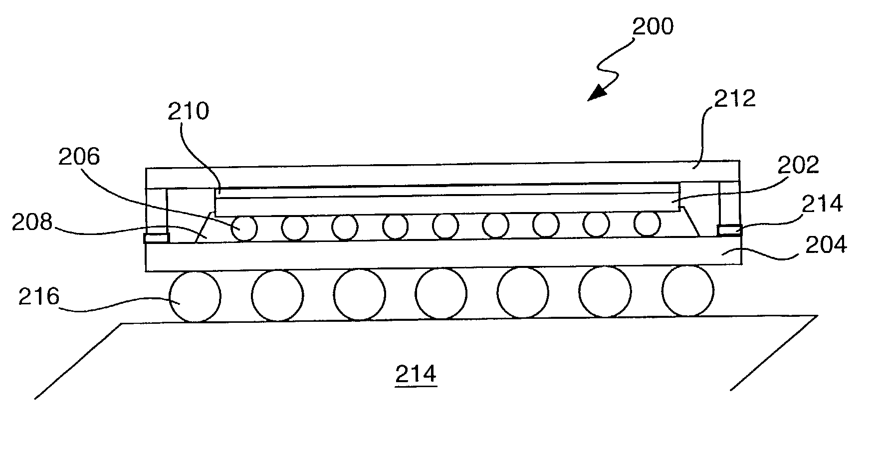
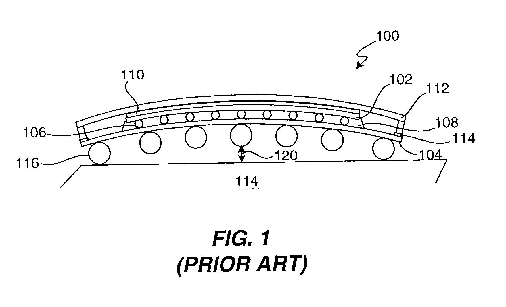
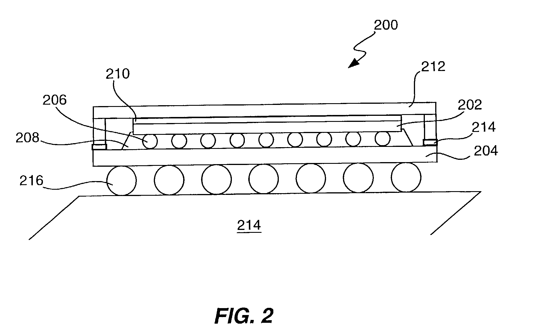
Flip chip package with warpage control
PatentInactiveUS6949404B1
Innovation
- The implementation of a heat spreader lid rigidly connected to the die or substrate with a balanced CTE and high shear strength adhesive, providing symmetrical bowing forces to counteract the CTE mismatch, thereby reducing or eliminating package bow and enhancing co-planarity.
Apparatus and method of printing solder on printed circuit board for warpage compensation
PatentPendingUS20250142735A1
Innovation
- A method involving the measurement of a chip package's warpage parameter, followed by the selection of a stencil configured to compensate for that warpage. The stencil is positioned above the PCB, and solder paste is applied through its apertures, allowing the PCB to be moved away before the chip package is attached.


Thermal Management Standards for Package Reliability
Thermal management standards for package reliability have evolved significantly to address the complex interplay between temperature variations and mechanical stress in semiconductor devices. The primary standards governing this domain include JEDEC JESD22-A104 for temperature cycling, IPC-9701A for board-level drop test methods, and JEDEC JESD22-B111 for board level temperature cycling. These standards establish critical temperature ranges, cycling parameters, and measurement protocols that directly influence warpage behavior in both chip packages and PCBs.
The JEDEC JESD22-A104 standard defines temperature cycling conditions ranging from -65°C to +150°C, with specific ramp rates and dwell times designed to simulate real-world thermal stress scenarios. This standard is particularly relevant to warpage analysis as it establishes the thermal boundaries within which package and PCB dimensional stability must be maintained. The cycling parameters directly correlate with coefficient of thermal expansion (CTE) mismatch effects between different materials in the assembly stack.
IPC-2221 and IPC-6012 standards provide comprehensive guidelines for PCB design and manufacturing tolerances that impact thermal performance. These standards specify maximum allowable bow and twist values for PCBs, typically limiting warpage to 0.75% of the diagonal length for surface mount applications. The thermal management aspects of these standards address copper distribution, via design, and layer stackup configurations that influence heat dissipation and thermal stress distribution.
Package-level thermal standards, including JEDEC JESD51 series, establish thermal characterization methodologies that directly impact reliability assessment. JESD51-2 defines integrated circuit thermal test method environmental conditions, while JESD51-14 provides transient dual interface test method guidelines. These standards enable accurate thermal resistance measurements that are essential for predicting warpage-induced reliability risks under various operating conditions.
The integration of thermal management standards with warpage control requires adherence to specific design rules and material selection criteria. Standards mandate the use of materials with compatible CTE values, typically within 2-3 ppm/°C difference between package substrate and PCB materials. Additionally, thermal interface material specifications under ASTM D5470 standard ensure proper heat transfer while minimizing mechanical stress that could exacerbate warpage issues and compromise long-term device reliability.
Material Selection Strategies for Warpage Minimization
Material selection represents the most fundamental approach to controlling warpage in chip packaging and PCB assemblies. The coefficient of thermal expansion (CTE) mismatch between different materials serves as the primary driver of warpage-induced stress during thermal cycling. Strategic material selection focuses on minimizing CTE differentials across the entire assembly stack, from die attach materials to substrate layers.
Substrate materials play a critical role in warpage control, with low-CTE options becoming increasingly important for advanced packaging applications. Bismaleimide triazine (BT) resins offer superior dimensional stability compared to traditional FR-4 materials, exhibiting CTE values ranging from 12-16 ppm/°C versus FR-4's 17-20 ppm/°C. For high-performance applications, ceramic substrates such as aluminum nitride (AlN) provide exceptional CTE matching with silicon dies, reducing thermal stress accumulation during operation.
Underfill materials require careful optimization to balance mechanical properties with thermal expansion characteristics. Modern underfill formulations incorporate silica fillers and specialized polymer matrices to achieve CTE values between 20-30 ppm/°C, creating a gradual transition zone between the silicon die and organic substrate. Advanced formulations utilize core-shell rubber particles and thermoplastic toughening agents to enhance fracture resistance while maintaining low shrinkage properties.
Mold compound selection significantly impacts package-level warpage behavior, particularly in overmolded assemblies. High-filler-content epoxy molding compounds with silica loadings exceeding 85% by weight demonstrate reduced CTE values and improved dimensional stability. Specialized grades incorporating spherical silica particles minimize viscosity increases while maximizing filler loading, enabling better flow characteristics during molding processes.
Die attach materials must provide both thermal and mechanical performance while minimizing CTE contributions to overall warpage. Silver-filled epoxy systems offer excellent thermal conductivity with moderate CTE values, while newer formulations incorporating thermally conductive ceramic fillers provide enhanced performance. Solder-based die attach solutions, particularly gold-tin eutectic systems, eliminate organic CTE contributions entirely but require careful thermal management during assembly.
Emerging material technologies focus on adaptive and smart material systems that respond dynamically to thermal stress conditions. Shape memory alloys integrated into package structures can provide active stress compensation, while gradient-index materials offer spatially varying CTE properties to optimize stress distribution across critical interfaces.
Unlock deeper insights with PatSnap Eureka Quick Research — get a full tech report to explore trends and direct your research. Try now!
Generate Your Research Report Instantly with AI Agent
Supercharge your innovation with PatSnap Eureka AI Agent Platform!