

Quantifying Chip Package Metallization Layer Peel Strength
APR 7, 20269 MIN READ
Generate Your Research Report Instantly with AI Agent
PatSnap Eureka helps you evaluate technical feasibility & market potential.
Chip Package Metallization Peel Strength Background and Objectives
Chip package metallization layers represent critical structural components in modern semiconductor devices, serving as the primary interface between the silicon die and external electrical connections. These thin metallic films, typically composed of materials such as aluminum, copper, or gold alloys, facilitate electrical conductivity while providing mechanical stability within the package assembly. The integrity of these metallization layers directly impacts device reliability, performance longevity, and overall system functionality.
The evolution of semiconductor packaging has witnessed a continuous trend toward miniaturization and increased functionality density. This progression has introduced unprecedented mechanical stresses on metallization layers, particularly during thermal cycling, mechanical shock, and long-term operational conditions. As package dimensions shrink and interconnect densities increase, the mechanical properties of these metallic interfaces become increasingly critical to device survival and performance maintenance.
Traditional reliability assessment methods have primarily focused on electrical characterization and thermal performance evaluation. However, the mechanical robustness of metallization layers has emerged as a fundamental limiting factor in advanced packaging technologies. Delamination, cracking, and adhesion failures at metallization interfaces represent significant failure modes that can compromise device functionality and reduce operational lifespan.
Current industry practices for evaluating metallization layer integrity often rely on qualitative assessment techniques or indirect measurement approaches. These methods frequently lack the precision and quantitative rigor necessary for comprehensive reliability prediction and process optimization. The absence of standardized quantitative measurement protocols has created significant challenges in establishing reliable design guidelines and quality control standards.
The primary objective of quantifying chip package metallization layer peel strength centers on developing robust, reproducible measurement methodologies that can accurately characterize the mechanical adhesion properties of these critical interfaces. This quantification effort aims to establish standardized testing protocols that enable precise comparison of different metallization materials, deposition processes, and interface treatments across various packaging platforms.
Furthermore, the development of quantitative peel strength measurement capabilities seeks to enable predictive reliability modeling for advanced packaging technologies. By establishing correlations between measured peel strength values and long-term reliability performance, engineers can optimize material selection, process parameters, and design configurations to maximize device durability and minimize field failure rates.
Market Demand for Reliable Semiconductor Packaging
The semiconductor packaging industry faces unprecedented demands for reliability as electronic devices become increasingly complex and mission-critical. Modern applications spanning automotive electronics, aerospace systems, medical devices, and high-performance computing require packaging solutions that can withstand extreme operating conditions while maintaining consistent performance over extended lifespans. The metallization layer peel strength represents a fundamental reliability parameter that directly impacts product longevity and field failure rates.
Market drivers for enhanced packaging reliability stem from multiple converging trends. The automotive sector's transition toward electric vehicles and autonomous driving systems demands semiconductor packages capable of operating reliably in harsh thermal and mechanical environments. These applications cannot tolerate packaging failures that could compromise safety-critical functions, creating stringent requirements for metallization layer adhesion performance.
Consumer electronics markets continue pushing for miniaturization while simultaneously increasing power densities and thermal cycling stresses. Advanced packaging technologies such as system-in-package configurations and heterogeneous integration place additional mechanical stresses on metallization layers, necessitating precise quantification methods to ensure adequate peel strength margins throughout product lifecycles.
The telecommunications infrastructure supporting 5G networks and edge computing requires semiconductor packages with exceptional reliability metrics. Network equipment manufacturers face substantial costs associated with field failures, driving demand for packaging solutions with quantifiable and predictable metallization layer performance characteristics.
Industrial automation and Internet of Things applications represent rapidly expanding market segments where packaging reliability directly correlates with system uptime and maintenance costs. These applications often operate in challenging environmental conditions with limited accessibility for repairs, making robust metallization layer adhesion essential for commercial viability.
Quality assurance requirements across all market segments increasingly emphasize statistical process control and predictive reliability modeling. Manufacturers require standardized methodologies for quantifying metallization layer peel strength to support design validation, production monitoring, and customer qualification processes. This market need drives development of advanced testing protocols and measurement technologies that can provide accurate, repeatable assessments of packaging reliability parameters.
Current State and Challenges in Metallization Adhesion Testing
The current landscape of metallization adhesion testing in semiconductor packaging presents a complex array of methodologies, each with distinct capabilities and limitations. Traditional mechanical testing approaches, including peel tests, pull tests, and shear tests, remain the industry standard for quantifying interfacial adhesion strength. However, these methods often struggle with reproducibility issues due to variations in sample preparation, loading conditions, and environmental factors.
Peel testing, specifically designed for measuring the force required to separate layered materials, faces significant challenges in semiconductor applications. The microscale dimensions of metallization layers, typically ranging from nanometers to micrometers in thickness, create substantial difficulties in achieving consistent grip attachment and uniform stress distribution during testing. Sample preparation becomes critical, as any surface contamination, oxidation, or mechanical damage can dramatically influence results.
Current testing standards, such as ASTM D903 and IPC-TM-650, were primarily developed for larger-scale applications and require substantial modifications for semiconductor metallization systems. The adaptation of these standards to chip package environments introduces uncertainties in measurement accuracy and inter-laboratory reproducibility. Many facilities report coefficient of variation values exceeding 20% for identical samples tested under supposedly identical conditions.
Advanced characterization techniques, including nanoindentation and atomic force microscopy-based methods, offer improved spatial resolution but introduce new complexities. These approaches often provide localized measurements that may not represent bulk adhesion behavior, particularly in heterogeneous metallization systems with varying grain structures and interfacial compositions.
Temperature and humidity control during testing represents another significant challenge. Metallization adhesion exhibits strong sensitivity to environmental conditions, with moisture absorption and thermal expansion effects potentially masking true interfacial strength characteristics. Many existing test protocols inadequately address these environmental dependencies.
The integration of real-time monitoring capabilities, such as acoustic emission detection and high-speed imaging, has improved understanding of failure mechanisms but has also revealed the complexity of adhesion failure modes. Multiple failure paths, including cohesive failure within metallization layers, interfacial delamination, and substrate cracking, often occur simultaneously, complicating result interpretation and correlation with field reliability data.
Existing Methods for Peel Strength Measurement
01 Surface treatment and roughening techniques for enhanced adhesion
Improving the peel strength of metallization layers in chip packages can be achieved through surface treatment methods such as plasma treatment, chemical etching, or mechanical roughening. These techniques modify the surface morphology and chemistry of the substrate, creating a rougher interface that promotes mechanical interlocking and chemical bonding between the metallization layer and the underlying material. The enhanced surface area and reactive sites facilitate stronger adhesion, reducing the risk of delamination during thermal cycling and mechanical stress.- Surface treatment and roughening techniques for enhanced adhesion: Surface treatment methods such as plasma treatment, chemical etching, or mechanical roughening can be applied to the substrate or metallization layer interface to improve peel strength. These techniques increase the surface area and create micro-mechanical interlocking between layers, resulting in stronger adhesion. The roughened surface provides better anchoring points for the metallization layer, reducing the risk of delamination during thermal cycling or mechanical stress.
- Adhesion promotion layers and interfacial materials: The incorporation of adhesion promotion layers or interfacial materials between the substrate and metallization layer significantly enhances peel strength. These intermediate layers can include titanium, chromium, or specialized polymer-based adhesion promoters that create strong chemical bonds with both the substrate and the metal layer. The adhesion layer acts as a bridge to reduce interfacial stress and improve overall bonding performance.
- Optimized metallization deposition parameters: Controlling deposition parameters such as temperature, pressure, deposition rate, and power during metallization processes like sputtering or electroplating can significantly affect peel strength. Optimized process conditions ensure better film density, reduced internal stress, and improved grain structure in the metallization layer. These factors contribute to enhanced mechanical properties and stronger adhesion to the underlying substrate.
- Multi-layer metallization structures with stress management: Implementing multi-layer metallization structures with alternating materials or varying compositions helps manage internal stress and improve peel strength. These structures can include stress-relief layers or gradient compositions that accommodate thermal expansion mismatches between different materials. The multi-layer approach distributes mechanical stress more evenly and prevents crack propagation at the interface.
- Post-deposition thermal treatment and annealing: Post-deposition thermal treatments such as annealing or heat treatment can enhance the peel strength of metallization layers by promoting interdiffusion at interfaces, relieving residual stress, and improving grain structure. These thermal processes allow for better atomic bonding between the metallization layer and substrate, resulting in improved mechanical integrity and resistance to delamination under operational conditions.
02 Use of adhesion promotion layers and interlayers
Incorporating adhesion promotion layers or interlayers between the substrate and metallization layer significantly improves peel strength. These intermediate layers, which may consist of materials with specific chemical compositions or structures, serve as a bridge to enhance bonding between dissimilar materials. They can reduce interfacial stress, accommodate thermal expansion mismatches, and provide additional bonding sites. The selection of appropriate interlayer materials and their thickness optimization are critical factors in achieving superior adhesion performance.Expand Specific Solutions03 Optimization of metallization deposition parameters
The peel strength of metallization layers is strongly influenced by deposition process parameters including temperature, pressure, deposition rate, and power settings. Optimizing these parameters during physical vapor deposition, chemical vapor deposition, or electroplating processes can control the microstructure, grain size, and internal stress of the metallization layer. Proper parameter selection results in denser films with fewer defects and better adhesion to the substrate. Post-deposition annealing treatments can further enhance adhesion by promoting interdiffusion and stress relief.Expand Specific Solutions04 Multi-layer metallization structures with graded compositions
Implementing multi-layer metallization structures with compositionally graded interfaces can effectively improve peel strength. By gradually transitioning the composition from the substrate material to the final metallization layer, interfacial stress concentrations are minimized and adhesion is enhanced. This approach allows for better accommodation of differences in thermal expansion coefficients and mechanical properties between layers. The graded structure distributes stress more uniformly across the interface, preventing crack initiation and propagation that lead to delamination.Expand Specific Solutions05 Testing and quality control methods for peel strength evaluation
Establishing robust testing protocols and quality control measures is essential for ensuring adequate metallization layer peel strength. Various mechanical testing methods including peel tests, pull tests, and shear tests can quantitatively assess adhesion strength. Non-destructive evaluation techniques such as acoustic microscopy and thermal imaging can detect interfacial defects before failure occurs. Implementing in-line monitoring during manufacturing processes enables real-time quality control and process adjustment to maintain consistent peel strength performance across production batches.Expand Specific Solutions
Key Players in Semiconductor Packaging and Testing Industry
The chip package metallization layer peel strength quantification field represents a mature but evolving technical domain within the broader semiconductor packaging industry. The market demonstrates significant scale, driven by increasing demand for reliable electronic devices across automotive, consumer electronics, and industrial applications. The competitive landscape features established materials science companies like Nitto Denko Corp., TDK Corp., and DuPont de Nemours, Inc., alongside major semiconductor manufacturers including Intel Corp., Advanced Micro Devices, Inc., and SMIC-Beijing. Technology maturity varies across players, with Japanese companies like Sumitomo Electric Industries Ltd. and LINTEC Corp. leading in advanced materials development, while Chinese foundries such as Semiconductor Manufacturing International (Shanghai) Corp. focus on manufacturing scale. The field benefits from cross-industry collaboration between packaging specialists like Xintec, Inc. and materials innovators, indicating a consolidating market where technical expertise in adhesion measurement and metallization processes determines competitive advantage.
Nitto Denko Corp.
Technical Solution: Nitto Denko has developed specialized adhesion testing solutions specifically designed for semiconductor packaging applications, focusing on quantifying peel strength of metallization layers through standardized 90-degree and 180-degree peel tests. Their methodology incorporates custom-designed test fixtures that accommodate various chip package geometries and sizes, with force measurement capabilities ranging from 0.01 to 100 N. The company's approach includes statistical analysis software that processes peel strength data to identify failure modes and optimize metallization processes for enhanced reliability.
Strengths: Specialized expertise in adhesion testing, flexible test fixture designs for various package types. Weaknesses: Limited to specific peel test configurations, may require customization for unique package designs.
Intel Corp.
Technical Solution: Intel employs advanced peel strength testing methodologies for their chip package metallization layers, utilizing precision mechanical testing equipment to measure adhesion forces between metal layers and substrate materials. Their approach combines standardized ASTM testing protocols with proprietary measurement techniques that can quantify peel strength values ranging from 0.1 to 50 N/mm. The company has developed automated testing systems that provide real-time monitoring of metallization layer integrity during manufacturing processes, ensuring consistent quality control across high-volume production lines.
Strengths: Industry-leading automation and precision measurement capabilities, extensive manufacturing experience. Weaknesses: High equipment costs and complex setup requirements for smaller scale operations.
Core Innovations in Metallization Adhesion Quantification
Peel strength simulating apparatus, peel strength simulating program storage medium, and peel strength simulating method
PatentInactiveUS7596477B2
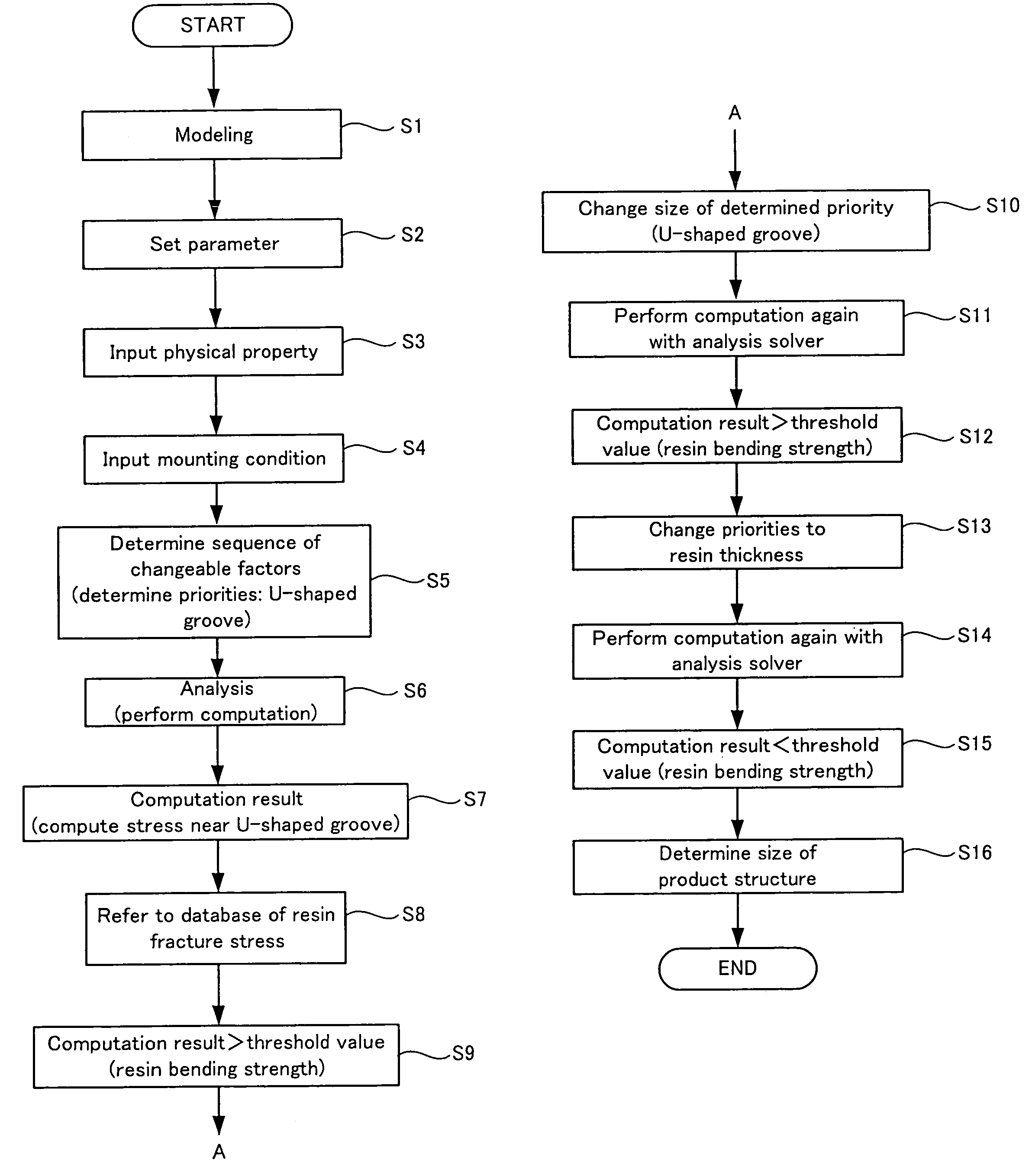
Innovation
- A peel strength simulating apparatus and method that adjusts various parameters such as size, material properties, and production conditions to simulate and enhance peel strength between the chip and resin package, ensuring the peel strength exceeds a predetermined threshold while minimizing cost increases.

Measurement method, peeling method, and peeling strength measuring apparatus
PatentPendingUS20240421006A1
Innovation
- A peeling method and apparatus using a blade with a first tool part having a first acute angle and a second tool part, where the first tool part is inserted along the substrate's surface toward the semiconductor chip's chamfered outer peripheral edge, and the second tool part applies a force away from the substrate to facilitate easy peeling, allowing measurement of bonding strength based on the peeling length.


Industry Standards for Semiconductor Package Reliability
The semiconductor industry has established comprehensive reliability standards to ensure package integrity throughout product lifecycles. These standards provide systematic frameworks for evaluating metallization layer adhesion strength, with organizations like JEDEC, IPC, and ASTM leading standardization efforts. JEDEC standards particularly focus on package-level reliability testing, while IPC standards address interconnect reliability requirements.
JEDEC JESD22 series standards form the backbone of semiconductor package reliability testing. JESD22-B117 specifically addresses die shear testing methodologies, while JESD22-B116 covers wire bond pull testing. These standards establish baseline requirements for metallization layer adhesion evaluation, defining test conditions, sample preparation protocols, and acceptance criteria. The standards mandate specific temperature cycling profiles, humidity exposure levels, and mechanical stress testing parameters.
IPC-9701A provides detailed guidelines for performance test methods and qualification requirements for surface mount solder attachments. This standard encompasses metallization layer integrity assessment through thermal cycling, mechanical shock, and vibration testing. The standard specifies minimum peel strength thresholds for different package types, ranging from 0.5 N/mm for fine-pitch components to 2.0 N/mm for high-power packages.
ASTM D6862 establishes standardized procedures for 90-degree peel adhesion testing of flexible substrates, directly applicable to flexible package metallization layers. The standard defines controlled peel rates, environmental conditioning requirements, and statistical analysis methods for adhesion strength quantification. Test specimens must undergo standardized conditioning at 23°C and 50% relative humidity for minimum 40 hours before testing.
Military standards MIL-STD-883 and MIL-STD-750 provide stringent reliability requirements for aerospace and defense applications. These standards mandate enhanced metallization layer adhesion testing under extreme environmental conditions, including temperature extremes from -65°C to +150°C, mechanical shock up to 1500G, and extended thermal cycling beyond commercial requirements.
Emerging standards development focuses on advanced packaging technologies including system-in-package and 3D integration architectures. New draft standards address through-silicon-via metallization reliability, wafer-level packaging adhesion requirements, and heterogeneous integration challenges. These evolving standards incorporate machine learning-based failure prediction models and real-time monitoring capabilities for next-generation reliability assessment methodologies.
Quality Control Integration in Manufacturing Process
The integration of peel strength quantification into manufacturing quality control systems represents a critical advancement in semiconductor packaging reliability. Modern manufacturing environments require real-time monitoring capabilities that can detect metallization layer adhesion defects before they propagate through the production line. This integration involves implementing automated testing protocols that seamlessly interface with existing manufacturing execution systems (MES) and statistical process control (SPC) frameworks.
Statistical process control implementation for peel strength monitoring requires establishing control limits based on historical performance data and customer reliability requirements. Control charts specifically designed for adhesion strength measurements enable operators to identify process drift before it results in field failures. The integration typically involves setting upper and lower specification limits at 3-sigma levels, with warning limits at 2-sigma to trigger preventive actions.
Automated data collection systems play a pivotal role in quality control integration, utilizing inline testing equipment that can perform peel strength measurements without disrupting production flow. These systems employ load cells and precision actuators integrated with vision systems to ensure consistent test positioning and force application. Data acquisition rates of up to 1000 samples per second enable comprehensive statistical analysis while maintaining production throughput requirements.
Real-time feedback mechanisms connect peel strength measurements directly to process control parameters, enabling immediate adjustments to deposition conditions, curing temperatures, or surface preparation protocols. Advanced manufacturing systems incorporate machine learning algorithms that can predict potential adhesion failures based on process parameter trends and historical correlation data.
Quality management system integration ensures that peel strength data becomes part of the comprehensive product quality record, enabling traceability from raw materials through final assembly. This integration supports regulatory compliance requirements and provides essential data for continuous improvement initiatives. The system architecture typically includes database integration with enterprise resource planning (ERP) systems and automated reporting capabilities for quality metrics dashboards.
Corrective action protocols triggered by out-of-specification peel strength measurements include automatic process holds, material quarantine procedures, and escalation pathways for engineering investigation. These protocols ensure that potential reliability issues are addressed immediately, preventing the shipment of potentially defective products while minimizing production disruption through targeted interventions.
Unlock deeper insights with PatSnap Eureka Quick Research — get a full tech report to explore trends and direct your research. Try now!
Generate Your Research Report Instantly with AI Agent
Supercharge your innovation with PatSnap Eureka AI Agent Platform!