

Compare Chip Package Substrate Materials for Better Integration
APR 7, 20269 MIN READ
Generate Your Research Report Instantly with AI Agent
PatSnap Eureka helps you evaluate technical feasibility & market potential.
Chip Package Substrate Evolution and Integration Goals
The evolution of chip package substrate materials has been driven by the relentless pursuit of higher performance, miniaturization, and enhanced functionality in electronic devices. From the early days of ceramic substrates in the 1960s to today's advanced organic and hybrid materials, substrate technology has undergone continuous transformation to meet increasingly demanding integration requirements. This evolution reflects the semiconductor industry's need to balance electrical performance, thermal management, mechanical reliability, and cost-effectiveness while enabling ever-smaller form factors.
Traditional ceramic substrates, primarily aluminum oxide and aluminum nitride, dominated early packaging applications due to their excellent thermal conductivity and dimensional stability. However, as circuit complexity increased and cost pressures mounted, organic substrates based on epoxy resins and polyimides gained prominence. These materials offered superior electrical properties for high-frequency applications and enabled finer pitch interconnections essential for advanced integrated circuits.
The integration goals for modern chip package substrates encompass multiple critical objectives that must be simultaneously achieved. Primary among these is the enhancement of electrical performance through reduced signal loss, minimized crosstalk, and improved power delivery efficiency. Advanced substrates must support increasingly dense interconnect structures while maintaining signal integrity across a broad frequency spectrum, particularly as data rates continue to escalate in applications ranging from 5G communications to artificial intelligence processors.
Thermal management represents another fundamental integration goal, as power densities in modern semiconductors continue to rise. Substrate materials must efficiently conduct heat away from active devices while maintaining structural integrity across wide temperature ranges. This requirement has driven the development of thermally enhanced organic substrates and hybrid solutions that combine the benefits of both organic and inorganic materials.
Mechanical reliability and dimensional stability constitute equally important objectives, particularly as package sizes shrink and component densities increase. Substrates must withstand thermal cycling, mechanical stress, and environmental conditions while maintaining precise dimensional tolerances necessary for reliable interconnections. The coefficient of thermal expansion matching between substrate and silicon die has become increasingly critical to prevent solder joint failures and ensure long-term reliability.
Cost optimization remains a persistent goal, driving the industry toward materials and processes that can deliver required performance levels while maintaining economic viability for high-volume production. This objective often necessitates trade-offs between performance characteristics and manufacturing complexity, leading to innovative material formulations and processing techniques that achieve optimal cost-performance ratios for specific application requirements.
Market Demand for Advanced Substrate Materials
The semiconductor packaging industry is experiencing unprecedented demand for advanced substrate materials driven by the rapid evolution of electronic devices and computing requirements. Consumer electronics, automotive systems, and data center infrastructure are pushing the boundaries of chip performance, necessitating substrate materials that can support higher frequencies, increased power densities, and enhanced thermal management capabilities.
Mobile device manufacturers are particularly driving demand for ultra-thin, high-density interconnect substrates that enable compact form factors while maintaining signal integrity. The proliferation of 5G technology has created substantial market pull for substrates capable of handling millimeter-wave frequencies with minimal signal loss. These applications require materials with low dielectric constants and dissipation factors that traditional organic substrates struggle to achieve.
The automotive sector represents a rapidly expanding market segment for advanced substrate materials, fueled by the electrification of vehicles and the integration of autonomous driving systems. Electric vehicles demand power electronics packages that can withstand extreme thermal cycling and high current densities, creating opportunities for ceramic and metal-core substrate technologies. Advanced driver assistance systems require radar and sensor modules with precise RF characteristics, driving adoption of specialized low-loss materials.
Data centers and high-performance computing applications are generating significant demand for substrates that can support advanced packaging techniques such as chiplet architectures and heterogeneous integration. These applications require materials capable of accommodating multiple die types with varying thermal expansion coefficients while maintaining reliable interconnections. The growing adoption of artificial intelligence accelerators and graphics processing units is particularly driving demand for substrates with superior thermal conductivity.
Emerging applications in Internet of Things devices, wearable electronics, and medical implants are creating new market segments for flexible and biocompatible substrate materials. These applications often require substrates that can conform to curved surfaces or withstand harsh environmental conditions while maintaining electrical performance.
The market is also responding to sustainability concerns, with increasing demand for substrate materials that support recycling initiatives and reduce environmental impact. This trend is driving research into bio-based organic materials and more efficient manufacturing processes that minimize waste generation.
Current Substrate Material Limitations and Challenges
Current chip package substrate materials face significant thermal management challenges that limit their effectiveness in high-performance applications. Traditional organic substrates, primarily composed of epoxy resin and glass fiber, exhibit poor thermal conductivity ranging from 0.3 to 0.8 W/mK. This inadequate heat dissipation capability creates thermal hotspots and reduces device reliability, particularly in power-intensive applications such as processors and graphics units. The thermal expansion mismatch between substrate materials and silicon chips further exacerbates these issues, leading to mechanical stress and potential failure points.
Electrical performance limitations represent another critical constraint in existing substrate technologies. Conventional FR-4 based substrates suffer from high dielectric loss at frequencies above 1 GHz, making them unsuitable for advanced RF and high-speed digital applications. The dielectric constant variations across temperature ranges cause signal integrity issues, while the relatively high loss tangent values contribute to power dissipation and signal degradation. These electrical limitations become increasingly problematic as chip operating frequencies continue to escalate.
Manufacturing complexity and cost considerations pose substantial barriers to substrate material optimization. Advanced materials such as low-temperature co-fired ceramics (LTCC) and liquid crystal polymers (LCP) offer superior electrical properties but require specialized processing equipment and techniques. The multi-layer fabrication processes demand precise control of via formation, layer alignment, and material compatibility, significantly increasing production costs and yield challenges. These manufacturing constraints limit the widespread adoption of high-performance substrate materials.
Mechanical reliability issues plague current substrate solutions, particularly in demanding environmental conditions. Organic substrates exhibit moisture absorption rates of 0.1-0.3%, leading to dimensional instability and delamination risks during reflow soldering processes. The coefficient of thermal expansion mismatch between different substrate layers creates internal stresses that can result in warpage, cracking, and interconnect failures. These mechanical limitations become more pronounced as package sizes increase and component densities rise.
Material compatibility challenges further complicate substrate selection and integration processes. The chemical interactions between different substrate materials, solder masks, and metallization layers can lead to adhesion failures and corrosion issues over time. Outgassing from organic materials can contaminate sensitive components, while material degradation under thermal cycling affects long-term reliability. These compatibility constraints require careful material selection and extensive qualification testing, adding complexity to the development process.
Mainstream Substrate Material Solutions Comparison
01 Advanced substrate materials for high-density interconnection
Integration of advanced substrate materials such as organic laminates, ceramic substrates, and composite materials to achieve high-density interconnection in chip packages. These materials provide improved electrical performance, thermal management, and mechanical stability for modern semiconductor packaging. The selection of appropriate substrate materials is critical for achieving miniaturization while maintaining signal integrity and reliability in high-performance applications.- Advanced substrate materials for high-density interconnection: Integration of advanced substrate materials enables high-density interconnection in chip packages. These materials provide improved electrical performance, thermal management, and mechanical stability. The substrates are designed to accommodate fine-pitch connections and support multiple layers of circuitry, allowing for compact package designs with enhanced signal integrity and reduced parasitic effects.
- Multi-layer substrate construction and lamination techniques: Multi-layer substrate construction involves stacking and laminating multiple dielectric and conductive layers to create complex interconnection structures. Advanced lamination techniques ensure proper bonding between layers while maintaining dimensional stability and electrical properties. These methods enable the integration of embedded components and facilitate the creation of high-performance package substrates with improved routing density and signal distribution capabilities.
- Thermal management integration in package substrates: Integration of thermal management features within package substrates addresses heat dissipation challenges in high-power applications. This includes the incorporation of thermal vias, heat spreaders, and thermally conductive materials into the substrate structure. The thermal management integration helps maintain optimal operating temperatures, improves reliability, and extends the lifespan of packaged semiconductor devices.
- Substrate material compatibility with flip-chip and wire bonding: Package substrate materials are engineered to be compatible with various interconnection methods including flip-chip bonding and wire bonding technologies. The materials must provide appropriate surface finishes, pad structures, and mechanical properties to support reliable connections. This compatibility ensures flexibility in package design and assembly processes while maintaining electrical performance and mechanical integrity across different bonding techniques.
- Organic and composite substrate material systems: Development of organic and composite substrate material systems offers cost-effective alternatives to traditional ceramic substrates while providing adequate electrical and mechanical properties. These materials include epoxy-based laminates, polyimide films, and reinforced composites that can be processed using standard manufacturing techniques. The material systems are designed to meet the requirements of various applications including consumer electronics, automotive, and telecommunications.
02 Multi-layer substrate structure integration
Development of multi-layer substrate structures that integrate various functional layers including dielectric layers, conductive layers, and via structures. This approach enables complex routing architectures and improved electrical characteristics through optimized layer stack-up designs. The integration of multiple layers allows for better space utilization and enhanced functionality in compact chip package designs.Expand Specific Solutions03 Thermal management substrate integration
Integration of thermal management features within substrate materials to enhance heat dissipation capabilities. This includes the use of thermally conductive materials, heat spreaders, and thermal vias embedded within the substrate structure. Effective thermal management through substrate design is essential for maintaining chip performance and reliability under high power operating conditions.Expand Specific Solutions04 Embedded component substrate technology
Integration of passive and active components directly into the substrate material to reduce package size and improve electrical performance. This technology involves embedding components such as capacitors, resistors, and even dies within the substrate layers, enabling system-in-package solutions. The embedded approach reduces interconnection lengths and improves overall system performance while achieving significant space savings.Expand Specific Solutions05 Substrate-to-chip interconnection methods
Development of advanced interconnection methods between substrate and chip including wire bonding, flip-chip, and through-silicon via technologies. These methods focus on achieving reliable electrical connections while minimizing parasitic effects and enabling high-speed signal transmission. The integration of optimized interconnection techniques with substrate materials is crucial for achieving high-performance chip packages with improved electrical characteristics and manufacturing yield.Expand Specific Solutions
Leading Substrate Material Suppliers and Manufacturers
The chip package substrate materials market represents a mature yet rapidly evolving sector driven by increasing demand for miniaturization and enhanced performance in semiconductor packaging. The industry is experiencing significant growth, with market expansion fueled by 5G, AI, and IoT applications requiring advanced substrate solutions. Technology maturity varies across players, with established semiconductor giants like Intel, Qualcomm, and Samsung Electronics leading in advanced packaging innovations, while specialized substrate manufacturers such as Nan Ya PCB, Siliconware Precision Industries, and LG Innotek focus on material optimization. Foundry leaders including GLOBALFOUNDRIES and SMIC are advancing substrate integration capabilities, while material suppliers like BASF and Merck Patent GmbH drive chemical innovations. Research institutions like IMEC and universities contribute fundamental breakthroughs, creating a competitive landscape where traditional boundaries between chipmakers, substrate manufacturers, and material suppliers increasingly blur as integration demands intensify.
QUALCOMM, Inc.
Technical Solution: Qualcomm focuses on advanced substrate materials optimized for RF and mixed-signal applications in mobile and wireless communication devices. Their substrate technology emphasizes low-loss dielectric materials with stable electrical properties across wide frequency ranges. Qualcomm has developed specialized substrate solutions incorporating liquid crystal polymer (LCP) and modified polyimide materials that provide excellent high-frequency performance while maintaining mechanical reliability. The company's substrate designs feature optimized stackup configurations with controlled impedance structures and integrated shielding capabilities, enabling better isolation between different functional blocks in complex system-on-package (SiP) implementations.
Strengths: Specialized expertise in RF substrate materials and high-frequency performance optimization. Weaknesses: Limited focus on general-purpose applications and dependency on external substrate manufacturers.
Intel Corp.
Technical Solution: Intel has developed advanced organic substrate materials with enhanced thermal management capabilities for their processor packages. Their substrate technology incorporates low-loss dielectric materials with optimized coefficient of thermal expansion (CTE) matching to silicon dies. Intel's substrate solutions feature multi-layer build-up structures with embedded passive components and fine-pitch interconnects supporting high-density I/O requirements. The company utilizes advanced materials like modified polyimide and liquid crystal polymer (LCP) substrates for high-frequency applications, enabling better signal integrity and reduced electromagnetic interference in complex multi-chip packages.
Strengths: Industry-leading thermal management and signal integrity solutions, extensive R&D capabilities. Weaknesses: High cost structure and complex manufacturing processes limiting scalability.
Key Innovations in High-Performance Substrate Materials
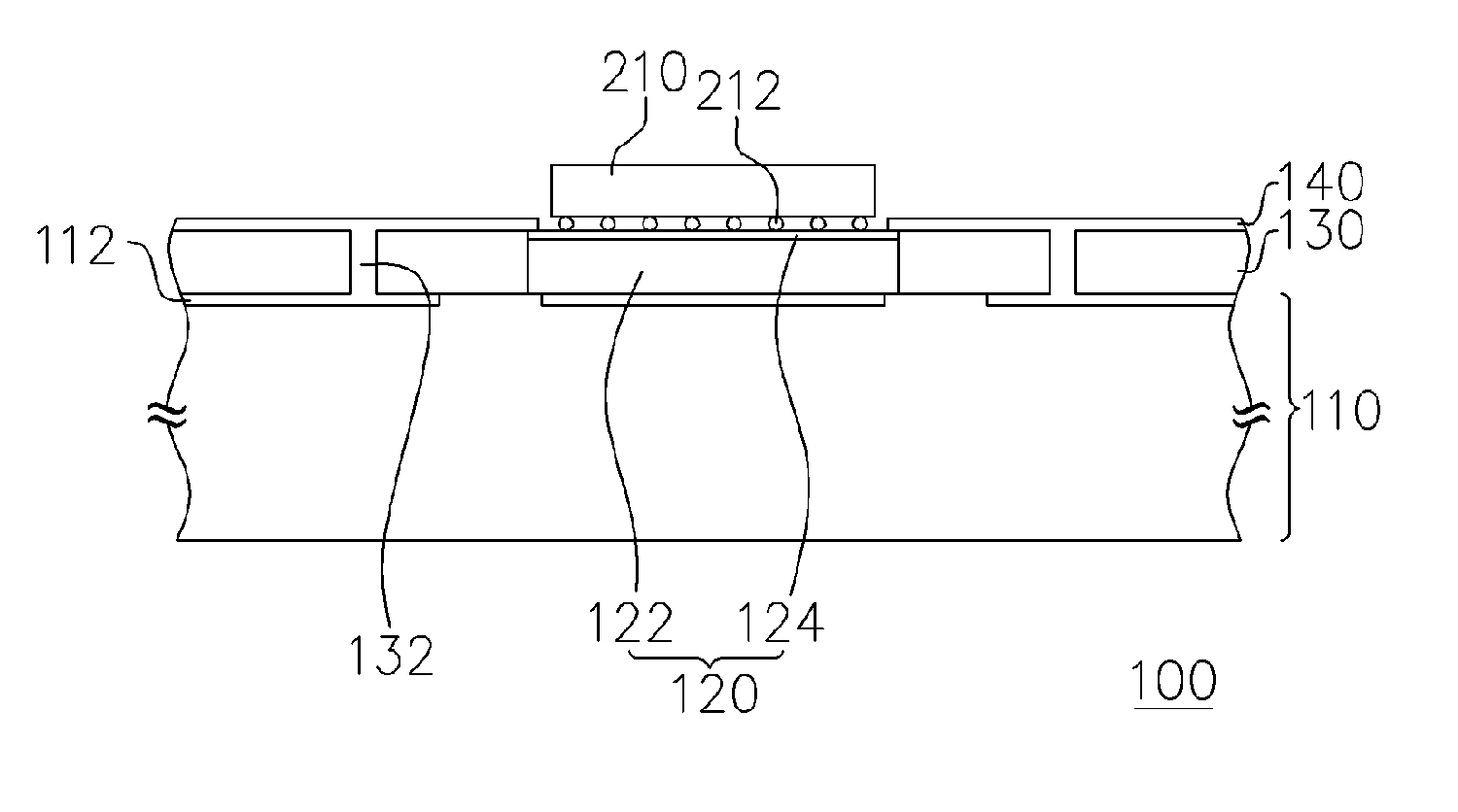
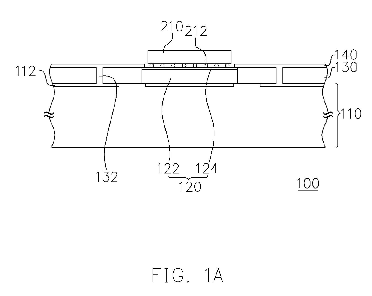
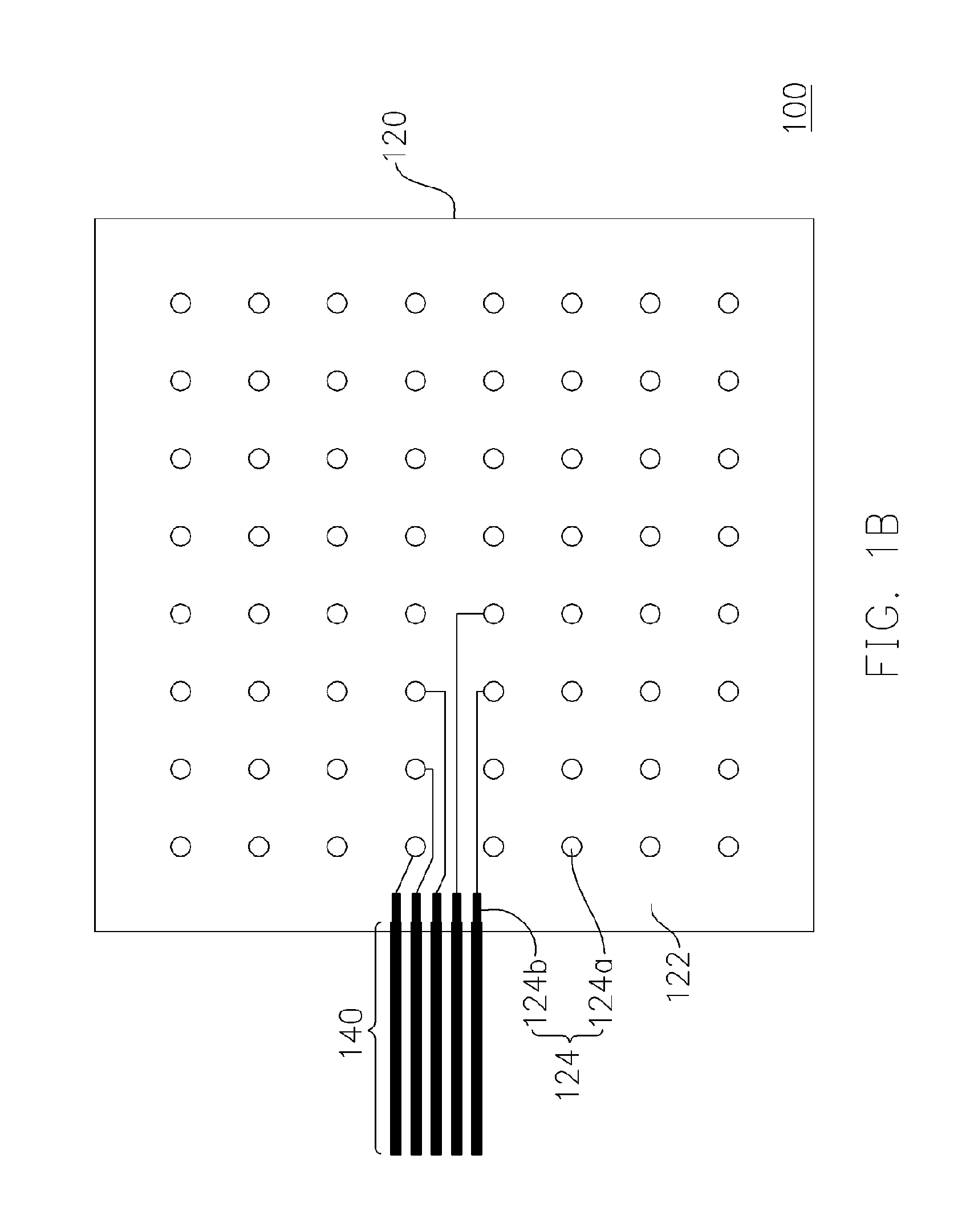
Chip package
PatentPendingUS20240120300A1
Innovation
- A chip package design utilizing a glass fiber substrate made of FR-4 fiberglass with a stacked metal substrate pad composed of nickel, palladium, and gold layers, or a nickel and gold layer stack, providing structural strength and reducing gold usage, while withstanding positive pressure during wire bonding.


Chip package structure, package substrate and manufacturing method thereof
PatentInactiveUS20060076659A1
Innovation
- A package substrate design incorporating an interposer with a second substrate and circuit layer, made of different materials than the first substrate, which allows for flexible bump pitch and reduced thermal stress by matching the thermal expansion coefficient of the chip, and includes a dielectric layer and conductive vias for electrical connectivity.

Thermal Management Considerations in Substrate Design
Thermal management represents one of the most critical design considerations in modern chip package substrate development, directly impacting device reliability, performance, and longevity. As semiconductor devices continue to shrink while power densities increase, the substrate's ability to efficiently dissipate heat becomes paramount for maintaining optimal operating conditions and preventing thermal-induced failures.
The thermal conductivity of substrate materials varies significantly across different options, fundamentally influencing heat dissipation capabilities. Ceramic substrates, particularly aluminum nitride and aluminum oxide, demonstrate superior thermal conductivity ranging from 20-180 W/mK, making them ideal for high-power applications. In contrast, organic substrates typically exhibit lower thermal conductivity values of 0.3-0.8 W/mK, requiring additional thermal management strategies such as embedded thermal vias or heat spreaders.
Coefficient of thermal expansion matching between substrate materials and semiconductor dies is crucial for preventing thermal stress-induced failures. Silicon-based substrates offer excellent CTE compatibility with silicon chips, minimizing thermal stress during temperature cycling. Organic substrates face greater challenges due to CTE mismatches, necessitating careful material selection and structural design optimization to accommodate thermal expansion differences.
Advanced thermal management techniques in substrate design include the integration of thermal interface materials, embedded cooling channels, and multi-layer thermal distribution networks. These approaches enable more effective heat spreading and removal, particularly important for high-performance computing and power electronics applications where thermal hotspots can significantly impact device performance.
The selection of substrate materials for thermal management must balance multiple factors including thermal conductivity, thermal capacity, manufacturing feasibility, and cost considerations. Glass-ceramic substrates emerge as promising compromise solutions, offering improved thermal properties compared to organic materials while maintaining reasonable manufacturing costs and design flexibility for complex integration requirements.
Environmental Impact of Substrate Manufacturing Processes
The environmental implications of chip package substrate manufacturing have become increasingly critical as the semiconductor industry faces mounting pressure to adopt sustainable practices. Traditional substrate manufacturing processes generate significant environmental burdens through energy-intensive production methods, chemical waste streams, and resource consumption patterns that challenge long-term sustainability goals.
Organic substrate manufacturing, particularly for build-up substrates using epoxy resin systems, involves multiple chemical processing steps that produce hazardous waste streams. The photolithography processes require toxic solvents and developers, while the electroplating operations generate heavy metal-containing effluents. These processes typically consume substantial amounts of water and energy, with manufacturing facilities requiring extensive wastewater treatment systems to meet environmental discharge standards.
Ceramic substrate production presents different environmental challenges, primarily related to high-temperature sintering processes that demand significant energy consumption. The firing of alumina and aluminum nitride substrates requires temperatures exceeding 1600°C, resulting in substantial carbon footprints. However, ceramic substrates offer superior longevity and recyclability compared to organic alternatives, potentially offsetting initial environmental costs through extended product lifecycles.
Glass substrate manufacturing involves melting processes at temperatures around 1000-1200°C, creating moderate energy demands compared to ceramics. The production of glass substrates generates fewer toxic byproducts than organic substrate manufacturing, though the energy-intensive melting and forming processes contribute to greenhouse gas emissions. Glass substrates also present advantages in terms of material recyclability and chemical stability.
Emerging sustainable manufacturing approaches focus on reducing solvent usage through dry processing techniques, implementing closed-loop water systems, and developing bio-based polymer alternatives for organic substrates. Advanced manufacturing facilities are increasingly adopting renewable energy sources and implementing circular economy principles to minimize waste generation and maximize material recovery rates.
The regulatory landscape continues to evolve, with stricter environmental standards driving innovation in cleaner production technologies. Life cycle assessment methodologies are becoming standard practice for evaluating the total environmental impact of different substrate materials, from raw material extraction through end-of-life disposal or recycling processes.
Unlock deeper insights with PatSnap Eureka Quick Research — get a full tech report to explore trends and direct your research. Try now!
Generate Your Research Report Instantly with AI Agent
Supercharge your innovation with PatSnap Eureka AI Agent Platform!