

Optimizing Chip Package PCB Pad Geometry for Connectivity Gains
APR 7, 20269 MIN READ
Generate Your Research Report Instantly with AI Agent
PatSnap Eureka helps you evaluate technical feasibility & market potential.
Chip Package PCB Evolution and Connectivity Targets
The evolution of chip package PCB technology has undergone significant transformation over the past three decades, driven by the relentless demand for higher performance, miniaturization, and enhanced connectivity. Early PCB designs in the 1990s featured relatively simple pad geometries with basic circular or rectangular shapes, primarily supporting through-hole and early surface-mount technologies. These initial designs were constrained by manufacturing limitations and focused on basic electrical connectivity rather than signal integrity optimization.
The transition to advanced packaging technologies marked a pivotal shift in PCB pad design philosophy. As semiconductor devices evolved from single-core processors to multi-core architectures and system-on-chip solutions, the complexity of interconnection requirements increased exponentially. This evolution necessitated more sophisticated pad geometries capable of supporting higher pin densities, improved thermal management, and enhanced electrical performance characteristics.
Modern chip package PCB development has been fundamentally shaped by the convergence of multiple technological drivers. The proliferation of mobile computing, artificial intelligence applications, and high-speed communication systems has created unprecedented demands for bandwidth, power efficiency, and form factor optimization. These market forces have directly influenced the evolution of pad geometry design, pushing engineers to develop innovative solutions that maximize connectivity while minimizing signal degradation and electromagnetic interference.
Contemporary connectivity targets have become increasingly ambitious, with industry standards now demanding support for multi-gigabit data rates, ultra-low latency communication, and power delivery capabilities exceeding 200 watts in compact form factors. The emergence of advanced packaging techniques such as chip-on-wafer-on-substrate and 2.5D/3D integration has further elevated the importance of optimized pad geometries as critical enablers of next-generation electronic systems.
The current technological landscape reflects a sophisticated understanding of the relationship between pad geometry optimization and overall system performance. Engineers now recognize that strategic pad design can significantly impact signal integrity, power distribution efficiency, thermal dissipation, and manufacturing yield. This recognition has established pad geometry optimization as a cornerstone technology for achieving ambitious connectivity targets in modern electronic systems, setting the foundation for continued innovation in high-performance computing and communication applications.
Market Demand for Enhanced PCB Connectivity Solutions
The global electronics industry is experiencing unprecedented demand for enhanced PCB connectivity solutions, driven by the rapid evolution of consumer electronics, automotive systems, and industrial applications. Modern electronic devices require increasingly sophisticated interconnection technologies to support higher data transmission rates, improved signal integrity, and enhanced power delivery capabilities. This growing complexity has created substantial market opportunities for advanced PCB pad geometry optimization technologies.
Consumer electronics manufacturers are particularly focused on miniaturization while maintaining or improving performance standards. Smartphones, tablets, and wearable devices demand PCB solutions that can accommodate higher component densities without compromising connectivity reliability. The proliferation of 5G technology has further intensified requirements for optimized pad geometries that can handle high-frequency signals with minimal loss and interference.
The automotive sector represents another significant growth driver for enhanced PCB connectivity solutions. Electric vehicles and autonomous driving systems require robust electronic architectures with superior connectivity performance. Advanced driver assistance systems, battery management units, and infotainment systems all depend on optimized PCB designs that can ensure reliable signal transmission under harsh operating conditions.
Data center and telecommunications infrastructure markets are experiencing substantial demand for high-performance PCB connectivity solutions. Cloud computing expansion and edge computing deployment require server hardware with exceptional signal integrity and thermal management capabilities. These applications necessitate precise pad geometry optimization to support high-speed data processing and transmission requirements.
Industrial automation and Internet of Things applications are creating additional market demand for reliable PCB connectivity solutions. Manufacturing equipment, sensor networks, and control systems require robust electronic connections that can operate reliably in challenging environmental conditions while maintaining consistent performance over extended operational periods.
Market research indicates strong growth potential for companies developing innovative PCB pad geometry optimization technologies. The increasing complexity of electronic systems, combined with stringent performance requirements across multiple industry sectors, has created a substantial addressable market for advanced connectivity solutions that can deliver measurable performance improvements through optimized design approaches.
Current PCB Pad Design Limitations and Challenges
Traditional PCB pad designs face significant geometric constraints that limit their ability to support high-density chip packaging requirements. Conventional circular and rectangular pad geometries often result in suboptimal electrical performance due to impedance mismatches and signal integrity issues. These standard shapes create discontinuities in signal paths, leading to reflection losses and reduced connectivity efficiency, particularly at higher frequencies where modern semiconductor devices operate.
Thermal management presents another critical limitation in current pad design approaches. Standard pad geometries frequently concentrate heat in localized areas, creating thermal hotspots that can compromise solder joint reliability and overall package performance. The inability to effectively distribute thermal loads across the pad surface results in temperature gradients that stress the interconnection materials and reduce long-term reliability of the chip-to-board interface.
Manufacturing tolerances impose strict constraints on achievable pad dimensions and spacing. Current lithographic processes limit the minimum feature sizes and aspect ratios that can be reliably produced, restricting designers' ability to optimize pad geometry for specific electrical requirements. These manufacturing limitations become increasingly problematic as chip packages demand finer pitch interconnections and higher I/O densities.
Signal crosstalk between adjacent pads represents a growing challenge in high-density packaging scenarios. Traditional pad layouts often lack adequate isolation mechanisms, allowing electromagnetic coupling between neighboring connections. This crosstalk degrades signal quality and limits the maximum achievable data rates, particularly in high-speed digital applications where signal integrity is paramount.
Mechanical stress concentration around conventional pad edges creates reliability concerns under thermal cycling and mechanical loading conditions. Sharp corners and abrupt geometry transitions in standard pad designs act as stress risers, potentially leading to solder joint fatigue and connection failures over the product lifecycle.
Current design methodologies also struggle with multi-layer routing complexity, where pad geometry must accommodate both surface connections and via transitions to internal layers. The three-dimensional nature of modern PCB designs requires pad shapes that can efficiently manage signal transitions between layers while maintaining controlled impedance characteristics throughout the interconnection path.
Current PCB Pad Geometry Optimization Methods
01 Pad geometry design for improved electrical connectivity
PCB pad geometry can be optimized through specific shapes, sizes, and configurations to enhance electrical connectivity and signal integrity. Various pad designs including circular, rectangular, oval, and custom geometries are employed to ensure reliable electrical connections between components and circuit traces. The geometry selection depends on component type, current requirements, and manufacturing constraints.- Pad geometry design for improved electrical connectivity: PCB pad geometry can be optimized through specific shapes, sizes, and configurations to enhance electrical connectivity and signal integrity. This includes designing pad dimensions, contours, and surface areas to ensure reliable solder joint formation and minimize contact resistance. Various geometric patterns such as circular, rectangular, or custom-shaped pads can be employed to accommodate different component types and mounting requirements.
- Multi-layer pad structures and via connections: Advanced PCB designs incorporate multi-layer pad structures with integrated via connections to establish electrical pathways between different circuit layers. These structures utilize through-hole vias, blind vias, or buried vias to create vertical interconnections while maintaining proper pad geometry at each layer. The design considerations include via placement relative to pad centers, annular ring dimensions, and thermal relief patterns to ensure robust connectivity throughout the board stack-up.
- Pad geometry for surface mount technology components: Specialized pad geometries are designed for surface mount technology applications, featuring precise dimensional tolerances and spacing to accommodate various component packages. These designs include considerations for solder paste deposition, component alignment, and reflow soldering processes. The pad layouts incorporate features such as solder mask openings, copper pad extensions, and optimized land patterns to ensure proper component placement and reliable solder joint formation.
- Thermal management in pad design: PCB pad geometry incorporates thermal management features to facilitate heat dissipation from components and improve overall thermal performance. This includes the integration of thermal pads, heat sink attachment areas, and thermal via arrays within or adjacent to component pads. The geometric design considers thermal conductivity paths, copper area distribution, and thermal relief patterns to balance electrical connectivity with effective heat transfer capabilities.
- Automated design and verification of pad connectivity: Modern PCB design methodologies employ automated tools and algorithms for designing and verifying pad geometry and connectivity. These systems analyze pad-to-trace connections, check for design rule violations, and optimize pad layouts for manufacturability. The verification processes include electrical connectivity testing, geometric dimension checking, and simulation of signal integrity to ensure that pad designs meet specified performance criteria before manufacturing.
02 Multi-layer pad structure and via connectivity
Advanced PCB designs utilize multi-layer pad structures with integrated via connections to establish electrical pathways between different layers. These structures incorporate through-hole vias, blind vias, or buried vias that connect pads across multiple layers, enabling complex routing and improved space utilization. The pad-via interface geometry is critical for maintaining signal integrity and reducing impedance mismatches.Expand Specific Solutions03 Thermal management through pad geometry optimization
Pad geometry plays a crucial role in thermal management by incorporating thermal relief patterns, heat dissipation structures, and optimized copper areas. Specialized pad designs include thermal vias, enlarged pad areas, and specific geometric patterns that facilitate heat transfer from components to the PCB substrate and surrounding layers. These designs help prevent component overheating and improve overall reliability.Expand Specific Solutions04 Solder joint reliability and pad geometry relationship
The geometry of PCB pads directly influences solder joint formation, strength, and long-term reliability. Optimized pad shapes and dimensions ensure proper solder wetting, adequate fillet formation, and mechanical stability. Design considerations include pad-to-component footprint matching, solder mask openings, and geometric features that prevent solder bridging while promoting consistent joint quality across manufacturing processes.Expand Specific Solutions05 High-frequency signal transmission and pad geometry
For high-frequency applications, pad geometry must be carefully designed to minimize signal reflection, crosstalk, and electromagnetic interference. Specialized pad configurations include controlled impedance designs, ground plane integration, and geometric features that maintain signal integrity at high frequencies. The pad shape, spacing, and connection to transmission lines are optimized to reduce parasitic capacitance and inductance effects.Expand Specific Solutions
Key Players in PCB and Semiconductor Packaging Industry
The chip package PCB pad geometry optimization market represents a mature yet evolving sector within the broader semiconductor packaging industry. The market demonstrates significant scale, driven by increasing demand for miniaturization and enhanced connectivity in electronic devices. Technology maturity varies considerably across market participants, with established leaders like Samsung Electronics, Intel, and NVIDIA driving advanced packaging innovations through sophisticated pad design methodologies. Asian manufacturers including SMIC, SK Hynix, and Advanced Semiconductor Engineering have achieved substantial technical capabilities in packaging solutions, while specialized companies like Himax Technologies and LG Innotek focus on display and component-specific applications. The competitive landscape shows consolidation around companies with integrated design-to-manufacturing capabilities, where pad geometry optimization directly impacts signal integrity, thermal management, and overall device performance in next-generation semiconductor packages.
Samsung Electronics Co., Ltd.
Technical Solution: Samsung has implemented sophisticated PCB pad geometry optimization strategies in their semiconductor packaging division, particularly for mobile processors and memory devices. Their approach combines advanced lithography techniques with precision etching to create optimized pad structures that enhance signal integrity and reduce crosstalk. Samsung's packaging solutions utilize fan-out wafer-level packaging (FOWLP) technology with carefully designed pad geometries that minimize parasitic effects while maximizing routing density. Their optimization methodology includes extensive use of 3D electromagnetic simulation tools to model pad-to-pad interactions and optimize via placement for improved electrical performance. The company has achieved notable success in reducing package size while maintaining or improving connectivity performance through innovative pad geometry designs.
Strengths: Strong integration capabilities across the entire semiconductor value chain and extensive experience in high-volume manufacturing. Weaknesses: Focus primarily on consumer electronics may limit applicability to specialized industrial or automotive applications.
Texas Instruments Incorporated
Technical Solution: Texas Instruments has developed comprehensive PCB pad geometry optimization solutions specifically tailored for analog and mixed-signal applications. Their approach emphasizes thermal management and electrical isolation through strategic pad placement and sizing. TI's packaging methodology incorporates advanced thermal interface materials with optimized pad geometries that enhance heat dissipation while maintaining signal integrity. Their design guidelines include detailed specifications for pad dimensions, solder mask openings, and via placement to minimize electromagnetic interference and improve overall system reliability. TI has pioneered the use of exposed thermal pads combined with optimized signal pad arrangements that provide superior thermal performance while reducing package footprint. Their solutions are particularly effective in power management applications where thermal considerations are critical.
Strengths: Deep expertise in analog circuit design and thermal management with strong focus on reliability and long-term performance. Weaknesses: Limited presence in high-speed digital applications compared to competitors, potentially restricting applicability in advanced computing systems.
Core Innovations in Advanced Pad Design Technologies
Optimized Circuit Design Layout for High Performance Ball Grid Array Packages
PatentInactiveUS20090170240A1
Innovation
- The layout of differential wiring pairs is optimized by ensuring maximum parallelism, equal length, and identical cross-sectional geometry, with traces spaced equally from the ground plane and controlled dielectric constant, to minimize these issues.


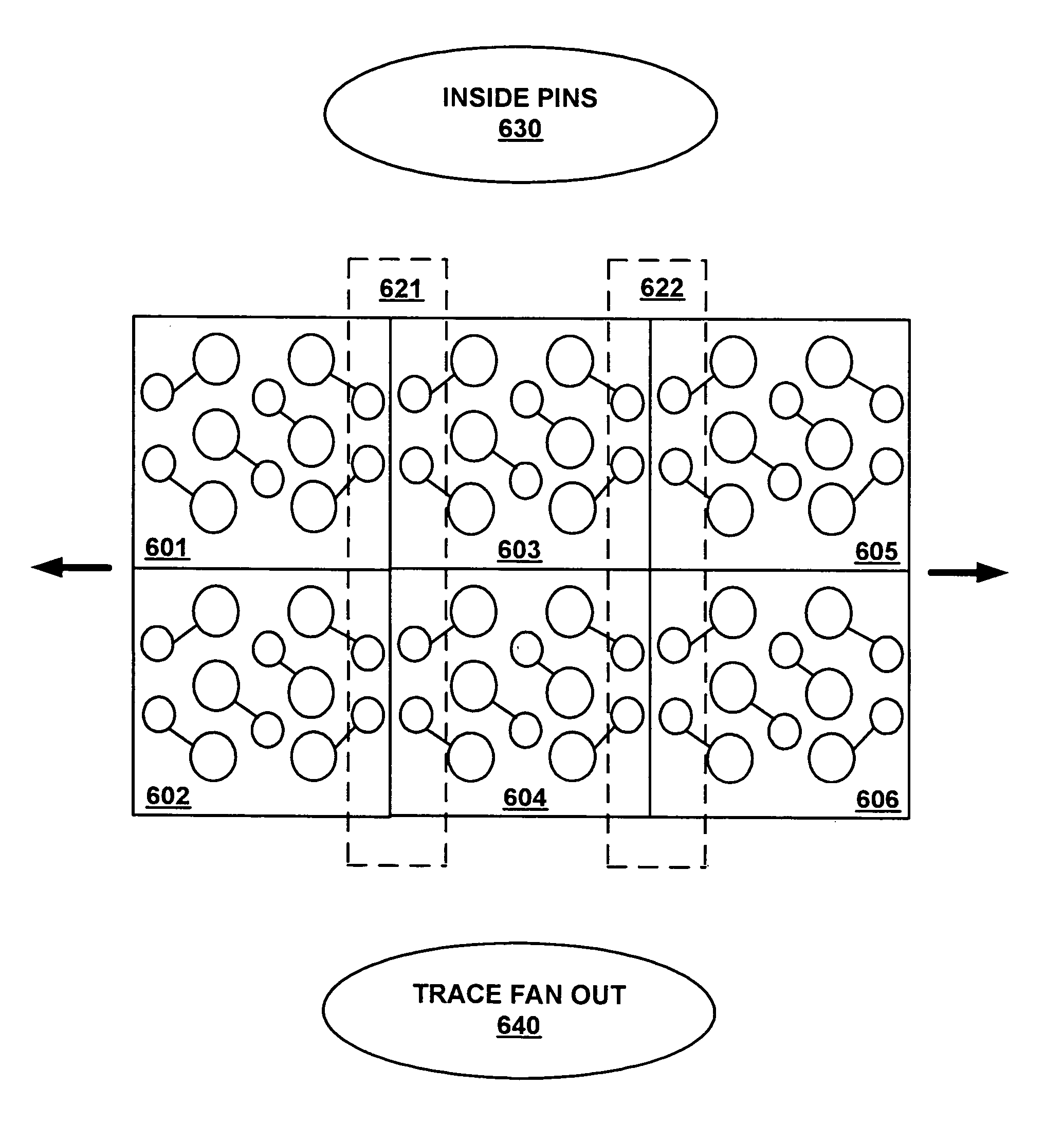
System for arraying surface mount grid array contact pads to optimize trace escape routing for a printed circuit board
PatentInactiveUS7161812B1
Innovation
- The implementation of a tiled arrangement of connection blocks with trace escape channels on the PCB, where the array of pins and vias are configured to minimize the impact of vias on trace routing, allowing for fewer PCB layers and improved copper plane arrangements for power and signal transmission.

Manufacturing Standards for PCB Design Compliance
The optimization of chip package PCB pad geometry for enhanced connectivity must operate within a comprehensive framework of manufacturing standards that ensure design compliance across the entire production lifecycle. These standards encompass dimensional tolerances, material specifications, and process control parameters that directly impact the feasibility and reliability of advanced pad geometries.
IPC standards, particularly IPC-2221 and IPC-2222, establish fundamental guidelines for PCB design that govern pad sizing, spacing, and geometric configurations. These standards define minimum annular ring requirements, via-to-pad relationships, and copper feature dimensions that must be maintained regardless of optimization objectives. Compliance with IPC-6012 qualification standards ensures that optimized pad geometries can be consistently manufactured while meeting electrical performance criteria.
Manufacturing process capabilities impose critical constraints on pad geometry optimization strategies. Standard PCB fabrication processes typically support minimum feature sizes of 75-100 micrometers for line width and spacing, with drill accuracy tolerances of ±50 micrometers. Advanced HDI manufacturing can achieve finer geometries down to 25-50 micrometers, but requires specialized equipment and process controls that impact cost and yield considerations.
Solder mask registration tolerances, typically ±75 micrometers, significantly influence pad geometry design decisions. Optimized pad shapes must account for these manufacturing variations to ensure proper solder mask opening alignment and prevent bridging or insufficient solder joint formation. Design rules must incorporate adequate safety margins while maximizing connectivity performance gains.
Surface finish specifications under IPC-4552 standards affect pad geometry optimization outcomes. Different surface finishes such as HASL, ENIG, or OSP exhibit varying thickness uniformities and planarity characteristics that influence optimal pad dimensions and shapes. Compliance requirements mandate consideration of finish thickness variations in pad geometry calculations.
Quality control standards including IPC-A-600 acceptability criteria establish inspection parameters for optimized pad geometries. These standards define acceptable limits for pad edge definition, copper adhesion, and dimensional accuracy that must be maintained throughout the optimization process. Statistical process control requirements ensure consistent reproduction of optimized geometries across production volumes.
Environmental compliance standards such as RoHS and REACH impose material restrictions that influence pad geometry optimization approaches. Lead-free soldering requirements affect thermal profiles and joint formation characteristics, necessitating pad geometry adjustments to maintain reliability while meeting regulatory compliance obligations.
Thermal Management in Optimized PCB Structures
Thermal management represents a critical consideration in optimized PCB pad geometries, as enhanced connectivity gains often come with increased power density and heat generation challenges. The geometric optimization of chip package PCB pads directly influences thermal dissipation pathways, requiring careful balance between electrical performance and thermal efficiency. Modern high-performance semiconductor packages generate substantial heat flux that must be effectively managed through strategic pad design and thermal interface optimization.
The relationship between pad geometry and thermal performance is multifaceted, involving conductive, convective, and radiative heat transfer mechanisms. Optimized pad configurations can serve dual purposes as electrical interconnects and thermal conduits, particularly when incorporating thermal vias and enhanced copper coverage areas. The thermal resistance from junction to ambient is significantly influenced by the pad-to-substrate interface design, where larger pad geometries generally provide improved thermal spreading but may compromise signal integrity in high-frequency applications.
Advanced thermal management strategies in optimized PCB structures include the implementation of thermal interface materials with enhanced conductivity, strategic placement of thermal vias beneath critical pads, and the integration of embedded cooling solutions. Copper pour optimization around pad areas creates effective heat spreading planes while maintaining electromagnetic compatibility. The thermal coefficient of expansion matching between pad materials and substrate becomes crucial in preventing thermal stress-induced failures during temperature cycling.
Emerging approaches focus on three-dimensional thermal management architectures that leverage optimized pad geometries as integral components of comprehensive cooling systems. These include micro-channel cooling integration, phase-change material incorporation, and active thermal management solutions that work synergistically with enhanced pad designs. The thermal modeling and simulation of these optimized structures require sophisticated computational fluid dynamics analysis to predict performance under various operating conditions.
Future developments in thermal management for optimized PCB structures will likely incorporate smart materials with adaptive thermal properties, advanced packaging techniques that integrate cooling directly into the pad geometry, and novel substrate materials with enhanced thermal conductivity while maintaining electrical performance requirements.
Unlock deeper insights with PatSnap Eureka Quick Research — get a full tech report to explore trends and direct your research. Try now!
Generate Your Research Report Instantly with AI Agent
Supercharge your innovation with PatSnap Eureka AI Agent Platform!