

How to Achieve Optimal Adhesion in Chip Package Stack Layers
APR 7, 20269 MIN READ
Generate Your Research Report Instantly with AI Agent
PatSnap Eureka helps you evaluate technical feasibility & market potential.
Chip Package Adhesion Background and Objectives
Chip packaging technology has undergone significant evolution since the early days of semiconductor manufacturing, transitioning from simple single-chip packages to complex multi-layer stack configurations. The progression from through-hole packages to surface-mount devices, and subsequently to advanced packaging solutions like System-in-Package (SiP) and 3D stacking, has fundamentally transformed the industry landscape. This evolution has been driven by the relentless pursuit of miniaturization, enhanced performance, and cost optimization in electronic devices.
The emergence of heterogeneous integration and chiplet architectures has further accelerated the demand for sophisticated packaging solutions. Modern electronic systems require the integration of diverse semiconductor technologies, including logic processors, memory devices, sensors, and RF components, within increasingly compact form factors. This integration challenge has positioned adhesion quality as a critical determinant of package reliability and performance.
Contemporary packaging approaches encompass various stacking methodologies, including wire bonding, flip-chip configurations, through-silicon vias (TSVs), and wafer-level packaging techniques. Each approach presents unique adhesion challenges related to material compatibility, thermal expansion mismatches, and mechanical stress distribution. The complexity is further amplified by the need to accommodate different die sizes, thicknesses, and material compositions within a single package assembly.
The primary technical objective centers on establishing robust interfacial bonding between dissimilar materials while maintaining structural integrity under diverse operational conditions. This encompasses achieving optimal adhesion strength to prevent delamination, ensuring uniform stress distribution to minimize warpage, and maintaining electrical connectivity throughout the package lifecycle. Additionally, the adhesion solution must accommodate thermal cycling, mechanical shock, and moisture exposure without compromising package performance.
Performance targets include achieving adhesion strengths exceeding industry standards for specific applications, minimizing interfacial void formation, and ensuring long-term reliability under accelerated aging conditions. The solution must also support manufacturing scalability while maintaining cost-effectiveness for high-volume production environments. These objectives collectively define the framework for developing next-generation adhesion technologies that can meet the evolving demands of advanced semiconductor packaging applications.
Market Demand for Advanced Chip Packaging Solutions
The semiconductor industry is experiencing unprecedented demand for advanced chip packaging solutions, driven by the relentless pursuit of higher performance, miniaturization, and functional integration across multiple technology sectors. This surge in demand stems from the fundamental shift toward heterogeneous integration, where different chip functionalities are combined within single packages to overcome the limitations of traditional monolithic scaling approaches.
Consumer electronics represent the largest market segment driving advanced packaging adoption. Smartphones, tablets, and wearable devices require increasingly sophisticated packaging technologies to accommodate multiple processors, memory modules, sensors, and communication chips within severely constrained form factors. The integration of artificial intelligence capabilities at the edge has further intensified requirements for high-density packaging solutions that can maintain reliable interconnections between diverse semiconductor components.
Data center and cloud computing infrastructure constitute another critical demand driver for advanced packaging technologies. The exponential growth in data processing requirements has created substantial market pressure for packaging solutions that can support high-bandwidth memory integration, advanced processor architectures, and efficient thermal management systems. Server processors increasingly rely on sophisticated packaging approaches to achieve the performance densities required for modern computational workloads.
Automotive electronics present rapidly expanding market opportunities for advanced packaging solutions, particularly with the acceleration of electric vehicle adoption and autonomous driving technologies. Modern vehicles incorporate hundreds of semiconductor devices requiring robust packaging that can withstand harsh environmental conditions while maintaining precise electrical performance. The automotive sector's reliability requirements have established stringent standards for adhesion quality and long-term package integrity.
The telecommunications infrastructure market, particularly with the global deployment of fifth-generation wireless networks, has generated substantial demand for advanced packaging technologies capable of supporting high-frequency operations and complex signal processing requirements. Base station equipment and network infrastructure components require packaging solutions that can maintain signal integrity while managing thermal dissipation effectively.
Emerging applications in artificial intelligence, machine learning accelerators, and quantum computing are creating new market segments with unique packaging requirements. These applications often demand novel approaches to chip stacking and interconnection that push the boundaries of conventional packaging technologies, creating opportunities for innovative adhesion solutions and advanced materials integration.
Current Adhesion Challenges in Multi-Layer Packaging
Multi-layer chip packaging faces significant adhesion challenges that directly impact device reliability and performance. The primary challenge stems from the inherent mismatch in thermal expansion coefficients between different materials used in the package stack. Silicon dies, organic substrates, metal interconnects, and polymer underfills each exhibit distinct thermal behaviors, creating interfacial stresses during temperature cycling that can lead to delamination and failure.
Interface contamination represents another critical challenge in achieving optimal adhesion. Organic residues, moisture, and oxidation layers can accumulate on bonding surfaces during manufacturing processes, significantly reducing the effectiveness of adhesive bonds. These contaminants are particularly problematic at the die-attach interface and between redistribution layers, where even microscopic contamination can compromise long-term reliability.
The complexity of modern package architectures introduces additional adhesion difficulties. Advanced packaging technologies such as 2.5D and 3D integration require multiple heterogeneous materials to be bonded in close proximity, creating a complex web of interfacial interactions. Each interface presents unique challenges related to surface energy matching, wettability, and chemical compatibility between adjacent layers.
Processing-related adhesion challenges arise from the sequential nature of package assembly. High-temperature processes required for subsequent layers can degrade previously formed adhesive bonds, leading to cumulative stress buildup and potential failure modes. The challenge is particularly acute in through-silicon-via structures where multiple thermal cycles are necessary for complete package formation.
Moisture sensitivity poses ongoing challenges for adhesion integrity. Hygroscopic materials within the package stack can absorb moisture during storage and handling, leading to vapor pressure buildup during reflow processes. This phenomenon, known as the popcorn effect, can cause catastrophic delamination at weak interfaces, particularly affecting polymer-based adhesive layers.
Scale-related challenges emerge as package dimensions continue to shrink while functional density increases. Achieving uniform adhesion across large die areas becomes increasingly difficult due to warpage and planarity issues. Additionally, the reduced bond line thickness in advanced packages demands extremely precise control of adhesive application and curing processes to maintain consistent interfacial properties.
Current Adhesion Solutions for Stack Layer Bonding
01 Adhesive layer composition and material selection
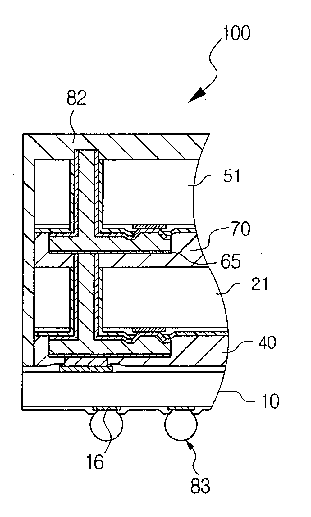
The adhesion between chip package stack layers can be improved through careful selection of adhesive materials and their composition. Various adhesive compositions including epoxy-based adhesives, thermoplastic adhesives, and modified resin systems can be formulated to enhance bonding strength between different layers in chip packages. The selection of appropriate adhesive materials with suitable viscosity, curing temperature, and mechanical properties is critical for achieving reliable layer-to-layer adhesion in stacked chip packages.- Use of adhesive layers between chip and substrate: Adhesive layers are applied between the chip and substrate to enhance bonding strength in stacked package structures. These adhesive materials provide mechanical stability and ensure reliable electrical connections. The adhesive composition and thickness are optimized to accommodate thermal expansion differences and prevent delamination during thermal cycling.
- Surface treatment and roughening techniques: Surface modification methods are employed to improve adhesion between stacked layers in chip packages. These techniques include plasma treatment, chemical etching, and mechanical roughening to increase surface area and enhance bonding characteristics. The treated surfaces provide better mechanical interlocking and chemical bonding with adhesive materials.
- Underfill materials for gap filling: Underfill materials are dispensed into gaps between stacked chips to improve adhesion and provide mechanical support. These materials flow into spaces and cure to form strong bonds while also protecting against moisture and contaminants. The underfill composition is formulated to match thermal expansion properties of adjacent materials and minimize stress concentration.
- Die attach films and thermal interface materials: Specialized die attach films and thermal interface materials are utilized to bond chip layers while facilitating heat dissipation. These materials combine adhesive properties with thermal conductivity to maintain junction temperatures within acceptable ranges. The film thickness and composition are controlled to optimize both mechanical adhesion and thermal performance.
- Molding compounds and encapsulation materials: Molding compounds are applied to encapsulate stacked chip structures and enhance overall package integrity. These materials provide protection against environmental factors while contributing to interlayer adhesion through compression and chemical bonding. The encapsulation process parameters are optimized to minimize voids and ensure uniform coverage across all stack layers.
02 Surface treatment and preparation methods
Surface treatment techniques play a crucial role in enhancing adhesion between chip package layers. Methods such as plasma treatment, chemical etching, surface roughening, and application of coupling agents can significantly improve the bonding interface. These surface modification techniques help to increase surface energy, remove contaminants, and create mechanical interlocking structures that promote stronger adhesion between stacked layers.Expand Specific Solutions03 Bonding process parameters and conditions
The adhesion quality between chip package stack layers is significantly influenced by bonding process parameters including temperature, pressure, time, and atmosphere control. Optimizing these parameters ensures proper curing of adhesives, minimizes void formation, and achieves uniform bonding across the interface. Process control methods such as staged heating, pressure profiling, and vacuum bonding can be employed to enhance layer adhesion and reduce defects.Expand Specific Solutions04 Interlayer structure design and configuration
The structural design of interlayer configurations affects adhesion performance in chip package stacks. Design considerations include the thickness of adhesive layers, the use of buffer layers, incorporation of reinforcement structures, and the arrangement of bonding patterns. Proper interlayer design helps to manage thermal expansion mismatch, reduce stress concentration, and improve overall adhesion reliability between stacked components.Expand Specific Solutions05 Adhesion testing and reliability evaluation
Various testing methods and reliability evaluation techniques are employed to assess the adhesion quality of chip package stack layers. These include mechanical testing such as die shear testing, pull testing, and peel testing, as well as reliability tests under thermal cycling, moisture exposure, and mechanical stress conditions. Comprehensive testing protocols help to ensure that the adhesion meets performance requirements and can withstand operational stresses throughout the product lifecycle.Expand Specific Solutions
Key Players in Semiconductor Packaging Industry
The chip package stack layer adhesion technology represents a mature yet rapidly evolving sector within the semiconductor packaging industry, currently valued at approximately $25 billion globally with projected growth driven by advanced 3D packaging demands. The competitive landscape is dominated by established players across three key segments: major semiconductor manufacturers like Samsung Electronics, Intel, Qualcomm, and SK Hynix who develop proprietary adhesion solutions for their products; specialized packaging service providers including Advanced Semiconductor Engineering, ChipMOS Technologies, STATS ChipPAC, and Siliconware Precision Industries who offer comprehensive turnkey solutions; and materials suppliers such as Henkel, LINTEC, and Mitsui Chemicals providing advanced adhesive formulations. Technology maturity varies significantly, with companies like Adeia Semiconductor Technologies and EV Group pushing cutting-edge direct bonding and hybrid bonding technologies, while traditional players focus on optimizing established adhesive methodologies for high-volume production applications.
Samsung Electronics Co., Ltd.
Technical Solution: Samsung employs advanced wafer-level packaging (WLP) technologies and through-silicon via (TSV) integration for optimal adhesion in chip package stack layers. Their approach utilizes proprietary underfill materials and die attach adhesives optimized for their memory and logic devices. Samsung's packaging solutions incorporate plasma surface treatment and chemical cleaning processes to enhance adhesion between different layers. The company has developed specialized bonding techniques for their 3D NAND and DRAM stacking technologies, utilizing temperature-controlled curing processes and precision dispensing systems. Their packaging methodology includes comprehensive adhesion testing protocols and reliability validation to ensure long-term performance in various operating conditions, particularly for mobile and automotive applications.
Strengths: Integrated manufacturing capabilities, extensive R&D resources, proven reliability in high-volume production. Weaknesses: Solutions primarily optimized for internal products, limited availability of technologies to external customers.
Advanced Semiconductor Engineering, Inc.
Technical Solution: ASE Group specializes in advanced packaging and test services, developing comprehensive solutions for chip package stack layer adhesion through their extensive portfolio of packaging technologies. Their approach includes flip-chip packaging, wafer-level packaging, and system-in-package (SiP) solutions that require precise adhesion control. ASE utilizes advanced underfill processes, die attach materials, and molding compounds specifically formulated for multi-layer package structures. The company employs sophisticated process control systems including automated dispensing equipment, controlled curing ovens, and real-time monitoring of adhesion parameters. Their solutions incorporate surface treatment technologies and material compatibility testing to ensure optimal bonding between different substrate materials and chip technologies across various applications including automotive, mobile, and IoT devices.
Strengths: Extensive packaging experience, high-volume manufacturing capabilities, comprehensive testing and validation services. Weaknesses: Primarily service-focused rather than materials development, dependent on third-party adhesive suppliers for core materials.
Core Adhesion Innovations in Package Stack Design
Stacked chip package using photosensitive polymer and manufacturing method thereof
PatentActiveUS20070048969A1
Innovation
- A photosensitive polymer layer is applied to the chips or wafers before stacking, partially cured for structural stability and adhesive retention, then fully cured to ensure complete gap filling and bonding between layers, enhancing adhesion and mechanical reliability.

Chip Attach Adhesive To Facilitate Embedded Chip Build Up And Related Systems And Methods
PatentInactiveEP2221860A3
Innovation
- A photosensitive, thermoset adhesive with reduced photoacid generator (PAG) levels and inclusion of thermal epoxy catalysts, antioxidants, and photo sensitizers to promote curing and prevent corrosion, while maintaining flexibility and reducing surface tackiness, is used in the ECBU process.


Reliability Standards for Chip Package Adhesion
Reliability standards for chip package adhesion have evolved significantly to address the increasing complexity of modern semiconductor packaging technologies. These standards establish critical benchmarks for evaluating adhesive performance under various environmental and operational conditions. The primary international standards include JEDEC JESD22 series, IPC standards, and ASTM test methods, which collectively define testing protocols for thermal cycling, moisture sensitivity, and mechanical stress evaluation.
Temperature cycling tests, as specified in JEDEC JESD22-A104, represent a fundamental reliability assessment method. These tests subject packaged devices to alternating high and low temperature extremes, typically ranging from -65°C to +150°C, to evaluate adhesive layer integrity under thermal stress. The standard defines specific ramp rates, dwell times, and cycle counts based on package complexity and intended application environments.
Moisture sensitivity level (MSL) classifications, outlined in JEDEC J-STD-020, establish critical parameters for adhesive performance in humid conditions. These standards categorize packages into six moisture sensitivity levels, with each level defining maximum floor life and baking requirements. Adhesive layers must maintain structural integrity and electrical isolation throughout specified moisture exposure periods without delamination or performance degradation.
Mechanical reliability standards focus on adhesive shear strength, peel strength, and die shear testing methodologies. ASTM D1002 and D3163 provide standardized approaches for measuring adhesive bond strength under controlled loading conditions. These tests evaluate the adhesive's ability to withstand mechanical stresses encountered during assembly, handling, and operational use.
Package-level reliability testing standards incorporate comprehensive stress combinations that simulate real-world operating conditions. Highly Accelerated Life Testing (HALT) and Highly Accelerated Stress Screening (HASS) protocols evaluate adhesive performance under combined thermal, mechanical, and electrical stresses. These standards ensure that adhesive systems maintain performance integrity throughout the product's intended operational lifetime.
Emerging reliability standards address advanced packaging technologies including 3D stacking, system-in-package configurations, and heterogeneous integration approaches. These evolving standards incorporate new test methodologies for evaluating adhesive performance in complex multi-layer structures where traditional testing approaches may prove insufficient for comprehensive reliability assessment.
Thermal Management Impact on Adhesion Performance
Thermal cycling represents one of the most critical factors affecting adhesion performance in chip package stack layers. During operational conditions, semiconductor packages experience repeated heating and cooling cycles that induce thermal stress at interfaces between different materials. The coefficient of thermal expansion (CTE) mismatch between silicon dies, organic substrates, and adhesive materials creates differential expansion and contraction rates, leading to interfacial shear and normal stresses that can compromise adhesion integrity over time.
The relationship between temperature and adhesion strength follows complex patterns that vary significantly across different adhesive chemistries. Epoxy-based underfills typically exhibit decreased adhesion strength at elevated temperatures due to polymer chain mobility increases and glass transition temperature effects. Conversely, some thermoplastic adhesives may show improved wetting and interfacial bonding at moderate temperature elevations, though excessive heat can lead to thermal degradation and bond failure.
Thermal gradient distribution within package stacks creates non-uniform stress fields that particularly challenge adhesion performance at critical interfaces. Hot spots generated by high-power semiconductor devices create localized thermal expansion zones, while peripheral areas remain at lower temperatures. This thermal non-uniformity results in complex stress distributions that can initiate delamination at weak interfacial points, propagating through the stack structure.
Moisture absorption combined with thermal cycling creates particularly challenging conditions for adhesion maintenance. Hygrothermal effects cause swelling in organic materials and can lead to hydrolysis of adhesive bonds, especially in silicone-based systems. The presence of moisture during thermal cycling accelerates interfacial degradation through steam pressure generation and chemical bond weakening mechanisms.
Advanced thermal management strategies directly influence adhesion longevity through stress mitigation approaches. Thermal interface materials with optimized CTE matching help reduce differential expansion stresses, while improved heat spreading techniques minimize thermal gradients. Package-level thermal design considerations, including heat sink placement and thermal via implementation, significantly impact the thermal environment experienced by adhesive interfaces, ultimately determining long-term reliability performance of the entire stack assembly.
Unlock deeper insights with PatSnap Eureka Quick Research — get a full tech report to explore trends and direct your research. Try now!
Generate Your Research Report Instantly with AI Agent
Supercharge your innovation with PatSnap Eureka AI Agent Platform!