

Compare EUV Lithography to E-Beam Lithography: Cost Implications
APR 2, 20269 MIN READ
Generate Your Research Report Instantly with AI Agent
PatSnap Eureka helps you evaluate technical feasibility & market potential.
EUV vs E-Beam Lithography Background and Objectives
Lithography technology represents the cornerstone of modern semiconductor manufacturing, enabling the precise patterning of integrated circuits at increasingly smaller dimensions. As the semiconductor industry continues its relentless pursuit of Moore's Law, the limitations of traditional optical lithography have necessitated the development of advanced patterning techniques capable of achieving sub-10nm feature sizes with the precision and reliability required for next-generation electronic devices.
Extreme Ultraviolet (EUV) lithography emerged as the industry's primary solution for high-volume manufacturing at advanced nodes, utilizing 13.5nm wavelength light to achieve unprecedented resolution capabilities. This technology represents a paradigm shift from conventional deep ultraviolet (DUV) lithography, requiring entirely new infrastructure, materials, and process methodologies. EUV lithography has become essential for producing leading-edge processors, memory devices, and system-on-chip solutions that power modern computing applications.
Electron Beam (E-beam) lithography, conversely, has established itself as a critical technology for mask making, prototyping, and specialized low-volume production applications. By directly writing patterns using focused electron beams, E-beam systems achieve exceptional resolution and flexibility, making them indispensable for research and development activities, photomask fabrication, and niche manufacturing requirements where design flexibility outweighs throughput considerations.
The fundamental objective of comparing these lithographic approaches centers on understanding their respective cost structures and economic implications for semiconductor manufacturing strategies. This analysis aims to evaluate the total cost of ownership, including capital equipment investments, operational expenses, yield considerations, and throughput capabilities that directly impact manufacturing economics.
Key technical objectives include assessing the scalability of each technology for different production volumes, examining the infrastructure requirements and associated costs, and evaluating the long-term viability of each approach for various semiconductor applications. The comparison seeks to identify optimal deployment scenarios where each technology provides maximum economic value while meeting stringent performance requirements.
Understanding these cost implications becomes crucial for strategic decision-making in semiconductor manufacturing, particularly as companies navigate the complex trade-offs between production flexibility, manufacturing volumes, and capital efficiency in an increasingly competitive global market environment.
Market Demand for Advanced Lithography Solutions
The semiconductor industry's relentless pursuit of smaller node geometries has created unprecedented demand for advanced lithography solutions capable of manufacturing chips at 7nm, 5nm, and beyond. This demand is primarily driven by the proliferation of high-performance computing applications, artificial intelligence processors, and mobile devices requiring increasingly sophisticated semiconductor architectures. Major foundries and integrated device manufacturers are investing heavily in next-generation lithography technologies to maintain competitive advantages in the global market.
Traditional optical lithography has reached fundamental physical limitations, creating a critical technology gap that advanced lithography solutions must address. The industry's transition toward extreme ultraviolet and electron beam lithography represents a paradigm shift necessitated by the inability of conventional deep ultraviolet systems to achieve the required resolution for advanced nodes. This technological inflection point has generated substantial market opportunities for companies developing cutting-edge lithography equipment and related infrastructure.
Market demand exhibits distinct characteristics across different application segments. High-volume manufacturing applications prioritize throughput efficiency and cost-effectiveness, driving interest in solutions that can process large quantities of wafers while maintaining precise pattern fidelity. Conversely, research and development applications, along with specialized low-volume production scenarios, demonstrate greater tolerance for slower processing speeds in exchange for superior resolution capabilities and design flexibility.
The automotive semiconductor sector has emerged as a significant demand driver, particularly with the accelerated adoption of electric vehicles and autonomous driving technologies. These applications require advanced processors manufactured using state-of-the-art lithography techniques, contributing to sustained market growth beyond traditional consumer electronics applications.
Geographically, demand concentration reflects the global semiconductor manufacturing landscape, with particularly strong requirements in regions hosting major foundries and memory manufacturers. The strategic importance of advanced lithography capabilities has also influenced government policies and investment priorities, further amplifying market demand through public-private partnerships and national semiconductor initiatives.
Supply chain considerations significantly impact market dynamics, as the complexity and specialized nature of advanced lithography equipment create dependencies on a limited number of suppliers. This supply constraint has intensified competition among semiconductor manufacturers seeking access to the most advanced lithography solutions, driving premium pricing and extended delivery timelines that reflect the critical nature of these technologies in enabling next-generation semiconductor production capabilities.
Current Cost Challenges in EUV and E-Beam Technologies
EUV lithography faces substantial cost challenges primarily stemming from its complex infrastructure requirements. The technology demands specialized light sources operating at 13.5 nanometer wavelengths, requiring sophisticated laser-produced plasma systems that consume enormous amounts of power. These EUV sources typically operate at only 2-5% efficiency, necessitating continuous maintenance and frequent component replacements. The mirrors used in EUV systems must maintain near-perfect reflectivity under extreme conditions, with each mirror set costing millions of dollars and requiring periodic refurbishment.
The manufacturing environment for EUV presents additional cost burdens through ultra-high vacuum requirements and contamination control systems. Any particle contamination can severely impact yield, demanding cleanroom facilities that exceed traditional semiconductor manufacturing standards. Pellicle technology, essential for protecting photomasks from contamination, remains technically challenging and expensive to implement at EUV wavelengths.
E-beam lithography encounters different but equally significant cost obstacles centered around throughput limitations. The serial writing process inherent to electron beam systems creates fundamental speed constraints, with typical throughput rates measured in wafers per day rather than wafers per hour. This low throughput directly translates to higher cost per wafer, making e-beam economically viable primarily for low-volume applications such as photomask production and research applications.
The precision required for e-beam systems introduces substantial equipment costs through ultra-stable mechanical platforms, sophisticated electron optics, and advanced beam control systems. These systems require constant calibration and environmental control to maintain nanometer-level accuracy. Additionally, the complexity of pattern data preparation and processing creates computational overhead that adds to operational expenses.
Both technologies share common cost challenges in resist chemistry optimization and process development. EUV requires specialized chemically amplified resists that can function effectively with limited photon flux, while e-beam systems need resists optimized for electron sensitivity. The development and qualification of these materials represent significant ongoing investments for both technology paths.
Maintenance costs constitute a major expense category for both technologies, though manifesting differently. EUV systems require frequent source maintenance and mirror cleaning cycles, while e-beam systems demand regular electron gun replacements and column maintenance. These operational requirements significantly impact total cost of ownership calculations for both lithography approaches.
Current Cost-Effective Lithography Solutions
01 Cost reduction through multi-beam lithography systems
Multi-beam lithography systems, particularly those using multiple electron beams in parallel, can significantly reduce manufacturing costs by increasing throughput. These systems allow simultaneous patterning of multiple areas, reducing the time required for wafer processing. The implementation of multi-column or multi-beam architectures enables higher productivity while maintaining pattern quality, making the technology more economically viable for high-volume manufacturing.- Cost reduction through hybrid lithography approaches: Combining EUV lithography with e-beam lithography in a hybrid approach can optimize manufacturing costs. This strategy leverages EUV for high-volume pattern transfer while using e-beam for critical dimension control and defect repair, reducing overall process costs. The hybrid methodology allows for selective application of each technology based on feature requirements, minimizing the use of expensive EUV exposure time while maintaining pattern fidelity.
- Throughput optimization for cost-effective EUV lithography: Improving throughput in EUV lithography systems directly impacts cost per wafer by reducing exposure time and increasing production volume. Advanced source power management, optimized resist sensitivity, and enhanced optical systems contribute to higher wafer processing rates. Multi-patterning techniques and computational lithography methods further enhance throughput while maintaining resolution requirements.
- E-beam direct write cost reduction through parallel processing: Multi-beam e-beam lithography systems reduce writing time and operational costs compared to single-beam systems. Parallel beam processing increases throughput significantly, making e-beam lithography more economically viable for mask making and small-volume production. Advanced beam control algorithms and optimized scanning strategies further enhance cost efficiency.
- Mask and reticle cost optimization: The cost of masks and reticles represents a significant portion of lithography expenses. Advanced mask repair techniques using focused ion beam or e-beam systems reduce mask replacement costs. Pellicle-free EUV masks and improved mask blank quality control minimize defects and extend mask lifetime, distributing costs over more wafer exposures.
- Process integration for reduced total cost of ownership: Integrated lithography solutions that combine pattern generation, inspection, and metrology reduce overall manufacturing costs. Optimized resist processing, reduced chemical consumption, and improved defect detection lower operational expenses. System automation and predictive maintenance strategies minimize downtime and extend equipment lifetime, improving total cost of ownership for both EUV and e-beam lithography systems.
02 Hybrid lithography approaches for cost optimization
Combining different lithography techniques, such as using electron beam lithography for critical layers and optical lithography for less critical layers, can optimize overall manufacturing costs. This hybrid approach leverages the high resolution of electron beam systems where needed while utilizing more cost-effective methods for other layers. The selective application of expensive lithography technologies based on feature criticality helps balance performance requirements with economic constraints.Expand Specific Solutions03 Throughput enhancement through advanced beam control
Advanced beam control mechanisms and optimization algorithms can improve the writing speed and efficiency of electron beam lithography systems, directly impacting cost-effectiveness. Techniques include optimized beam shaping, improved deflection systems, and intelligent pattern writing strategies that minimize beam movement and settling time. These enhancements reduce the time required per wafer, thereby lowering the cost per unit.Expand Specific Solutions04 Mask and maskless lithography cost considerations
The choice between mask-based and maskless lithography approaches significantly affects overall costs. Maskless electron beam direct write eliminates expensive mask fabrication but may have lower throughput. For EUV lithography, mask costs are substantial due to the complexity of multilayer reflective masks. Cost analysis must consider mask fabrication, inspection, repair costs, and the number of wafers to be processed to determine the most economical approach.Expand Specific Solutions05 Infrastructure and operational cost factors
The total cost of ownership for advanced lithography systems includes infrastructure requirements such as clean room specifications, power consumption, maintenance, and operational complexity. EUV systems require specialized facilities with precise environmental controls and high-power light sources, while electron beam systems need vacuum environments and sophisticated electron optics. Reducing these operational costs through improved system design, energy efficiency, and simplified maintenance procedures is crucial for commercial viability.Expand Specific Solutions
Major Lithography Equipment Manufacturers Analysis
The EUV versus E-beam lithography landscape represents a mature yet evolving semiconductor manufacturing sector with substantial market implications. The industry has reached advanced technological maturity, particularly in EUV adoption, driven by leading players like ASML Netherlands BV dominating EUV equipment supply and Taiwan Semiconductor Manufacturing Co., Ltd. leading high-volume production implementation. Major semiconductor manufacturers including Intel Corp. and Samsung Electronics Co., Ltd. have invested heavily in EUV infrastructure despite significantly higher capital costs compared to E-beam alternatives. While E-beam lithography, supported by companies like D2S Inc. and equipment providers such as Applied Materials Inc., offers lower initial investment requirements, it faces throughput limitations for mass production. The competitive dynamics show EUV commanding premium positioning for advanced node manufacturing, while E-beam maintains relevance in specialized applications and mask production, creating a bifurcated market structure with distinct cost-performance trade-offs.
Taiwan Semiconductor Manufacturing Co., Ltd.
Technical Solution: TSMC operates both EUV and e-beam lithography systems for different applications. For high-volume production nodes (7nm, 5nm, 3nm), TSMC relies heavily on ASML's EUV systems despite their $200+ million cost, as the superior throughput makes cost per wafer competitive at scale. For mask repair, critical dimension control, and low-volume specialty products, TSMC utilizes e-beam lithography which offers lower capital costs ($10-50 million) but significantly slower throughput. TSMC's cost analysis shows EUV becomes economically favorable when production volumes exceed certain thresholds, typically for leading-edge consumer processors.
Strengths: Extensive experience with both technologies, volume-based cost optimization, leading-edge process integration. Weaknesses: High dependency on expensive EUV infrastructure, complex technology transition costs.
ASML Netherlands BV
Technical Solution: ASML dominates the EUV lithography market as the sole supplier of EUV scanners, with systems costing $200-300 million each. Their Twinscan NXE series achieves 13.5nm wavelength lithography for sub-7nm node production. While EUV offers high throughput of 170+ wafers per hour for volume manufacturing, the capital expenditure is substantially higher than e-beam systems. ASML's EUV technology enables cost-effective mass production despite high initial investment, with cost per wafer decreasing significantly at high volumes due to superior throughput compared to e-beam's sequential writing approach.
Strengths: Market monopoly in EUV, high-volume manufacturing capability, established ecosystem. Weaknesses: Extremely high capital costs, complex infrastructure requirements, limited flexibility for prototyping.
Core Cost-Reduction Patents in Advanced Lithography
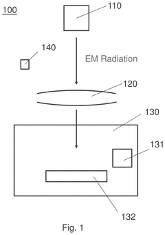
Methods and apparatus to reduce extreme ultraviolet light for photolithography
PatentPendingEP4625049A1
Innovation
- Employing a dual-dose exposure method using both UV and EUV light to sensitize the photoresist, reducing the EUV light dose needed for patterning by altering the solubility characteristics of the photoresist, thereby lowering energy and equipment costs.


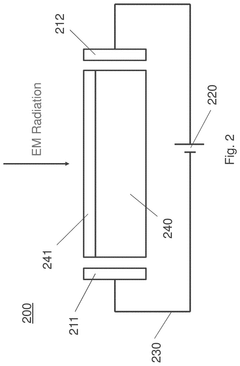
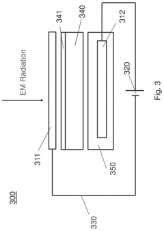
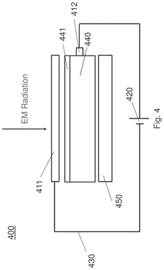
Methods and systems for electric field-assisted lithography
PatentPendingUS20250085639A1
Innovation
- The system comprises an electromagnetic radiation source, an optical assembly, and an exposure chamber with a substrate support and an electrode assembly that applies an electric field to an EM-sensitive layer on the semiconductor substrate during exposure to EUV radiation.
Semiconductor Industry Cost Regulations Impact
The semiconductor industry operates under a complex web of cost regulations that significantly influence the economic viability of advanced lithography technologies. These regulatory frameworks encompass environmental compliance standards, safety protocols, and international trade policies that directly impact the total cost of ownership for both EUV and E-beam lithography systems.
Environmental regulations impose substantial compliance costs on semiconductor manufacturers. EUV lithography systems require extensive environmental controls due to their use of hydrogen gas and tin plasma generation, necessitating specialized ventilation systems and waste management protocols. The regulatory requirements for handling and disposing of tin debris and hydrogen byproducts add operational complexity and ongoing compliance costs. E-beam lithography faces different environmental challenges, primarily related to electron beam safety regulations and electromagnetic interference shielding requirements.
Safety regulations significantly affect equipment design and operational procedures for both technologies. EUV systems must comply with stringent radiation safety standards, requiring specialized containment systems and personnel protection measures. The regulatory framework mandates regular safety audits, equipment certifications, and operator training programs, all contributing to increased operational costs. E-beam systems face similar safety regulations regarding electron beam exposure limits and require compliance with occupational safety standards for high-voltage equipment operation.
International trade regulations and export controls create additional cost implications for lithography equipment procurement and maintenance. Advanced lithography systems often fall under strategic technology export restrictions, affecting supply chain costs and service availability. These regulations can limit vendor options, increase procurement timelines, and elevate maintenance costs due to restricted access to specialized components and technical support.
Regulatory compliance reporting requirements impose ongoing administrative costs on semiconductor facilities. Both EUV and E-beam lithography operations must maintain detailed records of environmental emissions, safety incidents, and equipment performance metrics. The cost of regulatory compliance personnel, documentation systems, and periodic audits represents a significant portion of the total operational expenditure for advanced lithography facilities.
The evolving nature of semiconductor industry regulations creates uncertainty in long-term cost projections. As environmental standards become more stringent and safety requirements evolve, manufacturers must anticipate future compliance costs when evaluating lithography technology investments. This regulatory uncertainty particularly affects the economic comparison between EUV and E-beam lithography, as each technology faces different regulatory risk profiles and compliance cost trajectories.
Total Cost of Ownership Analysis Framework
The Total Cost of Ownership (TCO) analysis framework for comparing EUV and E-beam lithography requires a comprehensive multi-dimensional approach that extends beyond initial capital expenditure to encompass the entire operational lifecycle. This framework establishes standardized methodologies for evaluating both direct and indirect costs associated with each lithography technology over a defined time horizon, typically spanning 5-10 years to capture equipment depreciation cycles and technology evolution impacts.
Capital expenditure analysis forms the foundation layer, incorporating equipment acquisition costs, facility infrastructure modifications, and installation expenses. EUV systems demand substantial upfront investments ranging from $200-300 million per tool, while E-beam systems vary significantly based on throughput requirements, from $10-50 million for advanced multi-beam configurations. Infrastructure costs differ markedly, with EUV requiring specialized clean room environments, hydrogen safety systems, and high-power electrical installations.
Operational expenditure evaluation encompasses consumables, maintenance, utilities, and labor costs. EUV systems consume expensive photoresists, pellicles, and require frequent source maintenance, while E-beam systems incur costs through electron source replacements and column maintenance. Energy consumption patterns differ substantially, with EUV systems requiring continuous high-power operation versus E-beam systems' variable power consumption based on pattern complexity.
Productivity metrics integration translates technical performance into economic impact through throughput analysis, yield considerations, and defect-related costs. EUV achieves superior throughput for high-volume production but faces availability challenges due to source reliability. E-beam systems offer deterministic patterning with minimal defects but suffer from inherently lower throughput, making them suitable for low-volume, high-mix applications.
Risk assessment components address technology maturity, supply chain dependencies, and obsolescence factors. EUV technology carries risks related to source availability and mask infrastructure, while E-beam systems face challenges in scaling throughput for volume manufacturing. The framework incorporates sensitivity analysis to evaluate cost implications under various production scenarios and technology advancement trajectories.
Unlock deeper insights with PatSnap Eureka Quick Research — get a full tech report to explore trends and direct your research. Try now!
Generate Your Research Report Instantly with AI Agent
Supercharge your innovation with PatSnap Eureka AI Agent Platform!