

Compare Mechanical Flexibility in Wafer Reconstitution vs Embedding
APR 21, 20269 MIN READ
Generate Your Research Report Instantly with AI Agent
PatSnap Eureka helps you evaluate technical feasibility & market potential.
Wafer Reconstitution vs Embedding Technology Background and Goals
Wafer-level packaging technologies have undergone significant evolution over the past two decades, driven by the relentless demand for miniaturization, enhanced performance, and cost-effective manufacturing in semiconductor devices. The emergence of advanced packaging solutions has fundamentally transformed how electronic components are integrated, particularly in applications requiring high-density interconnections and superior mechanical properties.
Wafer reconstitution technology emerged in the early 2000s as a revolutionary approach to address the limitations of traditional packaging methods. This technique involves the assembly of individual dies onto a carrier substrate, followed by molding compound encapsulation to create a reconstituted wafer format. The process enables the handling of heterogeneous components and different die sizes within a single package, offering unprecedented flexibility in system integration.
Embedding technology, conversely, represents a paradigm shift toward true three-dimensional integration. This approach involves the direct placement of active and passive components within the substrate layers, creating embedded systems that achieve remarkable space efficiency. The technology has gained substantial traction in applications where mechanical robustness and thermal management are critical considerations.
The mechanical flexibility comparison between these two approaches has become increasingly relevant as electronic devices face more demanding operational environments. Modern applications in automotive, aerospace, and wearable electronics require packaging solutions that can withstand mechanical stress, thermal cycling, and dynamic loading conditions while maintaining electrical integrity.
The primary technical objective centers on understanding how each technology responds to mechanical deformation, stress distribution, and long-term reliability under various loading conditions. Wafer reconstitution typically exhibits different mechanical behavior due to the presence of molding compounds and the interface characteristics between dies and carrier substrates. The stress concentration patterns and failure modes in reconstituted structures often differ significantly from embedded configurations.
Embedding technology aims to achieve superior mechanical integration by eliminating traditional packaging interfaces and creating monolithic structures. The embedded components experience stress distribution patterns that are more closely coupled to the substrate mechanical properties, potentially offering enhanced reliability under certain loading scenarios.
Current research focuses on developing comprehensive mechanical characterization methodologies that can accurately predict the performance of both technologies under real-world operating conditions. Advanced finite element modeling, coupled with experimental validation through mechanical testing protocols, forms the foundation for understanding the comparative advantages and limitations of each approach in terms of mechanical flexibility and long-term durability.
Wafer reconstitution technology emerged in the early 2000s as a revolutionary approach to address the limitations of traditional packaging methods. This technique involves the assembly of individual dies onto a carrier substrate, followed by molding compound encapsulation to create a reconstituted wafer format. The process enables the handling of heterogeneous components and different die sizes within a single package, offering unprecedented flexibility in system integration.
Embedding technology, conversely, represents a paradigm shift toward true three-dimensional integration. This approach involves the direct placement of active and passive components within the substrate layers, creating embedded systems that achieve remarkable space efficiency. The technology has gained substantial traction in applications where mechanical robustness and thermal management are critical considerations.
The mechanical flexibility comparison between these two approaches has become increasingly relevant as electronic devices face more demanding operational environments. Modern applications in automotive, aerospace, and wearable electronics require packaging solutions that can withstand mechanical stress, thermal cycling, and dynamic loading conditions while maintaining electrical integrity.
The primary technical objective centers on understanding how each technology responds to mechanical deformation, stress distribution, and long-term reliability under various loading conditions. Wafer reconstitution typically exhibits different mechanical behavior due to the presence of molding compounds and the interface characteristics between dies and carrier substrates. The stress concentration patterns and failure modes in reconstituted structures often differ significantly from embedded configurations.
Embedding technology aims to achieve superior mechanical integration by eliminating traditional packaging interfaces and creating monolithic structures. The embedded components experience stress distribution patterns that are more closely coupled to the substrate mechanical properties, potentially offering enhanced reliability under certain loading scenarios.
Current research focuses on developing comprehensive mechanical characterization methodologies that can accurately predict the performance of both technologies under real-world operating conditions. Advanced finite element modeling, coupled with experimental validation through mechanical testing protocols, forms the foundation for understanding the comparative advantages and limitations of each approach in terms of mechanical flexibility and long-term durability.
Market Demand for Advanced Wafer-Level Packaging Solutions
The semiconductor industry is experiencing unprecedented demand for advanced wafer-level packaging solutions, driven by the relentless pursuit of miniaturization, enhanced performance, and cost optimization across multiple application domains. Consumer electronics, automotive systems, telecommunications infrastructure, and emerging technologies such as artificial intelligence and Internet of Things devices are collectively pushing the boundaries of traditional packaging approaches.
Mobile devices continue to serve as primary catalysts for packaging innovation, requiring increasingly sophisticated solutions that can accommodate multiple functionalities within severely constrained form factors. The integration of advanced sensors, high-performance processors, memory modules, and wireless communication components necessitates packaging technologies that can deliver superior electrical performance while maintaining mechanical reliability under diverse operating conditions.
Automotive electronics represent another significant growth driver, particularly with the accelerating adoption of electric vehicles and autonomous driving systems. These applications demand packaging solutions that can withstand extreme temperature variations, mechanical stress, and long-term reliability requirements that far exceed consumer electronics standards. The mechanical flexibility characteristics of different packaging approaches become critical factors in meeting these stringent automotive qualification requirements.
Data center and high-performance computing applications are increasingly adopting advanced packaging technologies to address thermal management challenges and achieve higher bandwidth densities. The mechanical properties of wafer-level packaging solutions directly impact their ability to handle thermal cycling stress and maintain signal integrity under high-power operating conditions.
The telecommunications sector, particularly with the ongoing deployment of fifth-generation wireless networks, requires packaging solutions that can support higher frequencies while maintaining cost-effectiveness for mass deployment. The mechanical flexibility differences between reconstitution and embedding approaches significantly influence their suitability for radio frequency applications where mechanical stability directly affects electrical performance.
Emerging applications in wearable devices, medical implants, and flexible electronics are creating new market segments that prioritize mechanical adaptability and reliability. These applications often require packaging solutions that can conform to non-planar surfaces or withstand repeated mechanical deformation, making the comparative mechanical flexibility of different wafer-level packaging approaches a crucial selection criterion for design engineers and product developers.
Mobile devices continue to serve as primary catalysts for packaging innovation, requiring increasingly sophisticated solutions that can accommodate multiple functionalities within severely constrained form factors. The integration of advanced sensors, high-performance processors, memory modules, and wireless communication components necessitates packaging technologies that can deliver superior electrical performance while maintaining mechanical reliability under diverse operating conditions.
Automotive electronics represent another significant growth driver, particularly with the accelerating adoption of electric vehicles and autonomous driving systems. These applications demand packaging solutions that can withstand extreme temperature variations, mechanical stress, and long-term reliability requirements that far exceed consumer electronics standards. The mechanical flexibility characteristics of different packaging approaches become critical factors in meeting these stringent automotive qualification requirements.
Data center and high-performance computing applications are increasingly adopting advanced packaging technologies to address thermal management challenges and achieve higher bandwidth densities. The mechanical properties of wafer-level packaging solutions directly impact their ability to handle thermal cycling stress and maintain signal integrity under high-power operating conditions.
The telecommunications sector, particularly with the ongoing deployment of fifth-generation wireless networks, requires packaging solutions that can support higher frequencies while maintaining cost-effectiveness for mass deployment. The mechanical flexibility differences between reconstitution and embedding approaches significantly influence their suitability for radio frequency applications where mechanical stability directly affects electrical performance.
Emerging applications in wearable devices, medical implants, and flexible electronics are creating new market segments that prioritize mechanical adaptability and reliability. These applications often require packaging solutions that can conform to non-planar surfaces or withstand repeated mechanical deformation, making the comparative mechanical flexibility of different wafer-level packaging approaches a crucial selection criterion for design engineers and product developers.
Current State and Mechanical Flexibility Challenges
The semiconductor packaging industry currently faces significant mechanical flexibility challenges when implementing advanced packaging technologies, particularly in wafer-level packaging approaches. Both wafer reconstitution and embedding techniques have emerged as critical solutions for achieving higher integration density and improved performance, yet each approach presents distinct mechanical stress profiles and flexibility limitations that impact device reliability and manufacturing yield.
Wafer reconstitution technology encounters substantial mechanical challenges primarily related to coefficient of thermal expansion (CTE) mismatches between different materials in the reconstructed wafer stack. The process involves mounting individual dies onto a temporary carrier substrate, followed by molding compound encapsulation and subsequent processing steps. During thermal cycling, the CTE differences between silicon dies, molding compounds, and carrier substrates generate significant mechanical stress concentrations at interfaces, leading to potential delamination, cracking, and warpage issues.
Current wafer reconstitution implementations struggle with maintaining uniform stress distribution across large panel sizes, particularly when processing dies of varying thicknesses or materials. The mechanical flexibility is further constrained by the limited elastic modulus range of available molding compounds, which must balance between providing adequate mechanical support during processing while minimizing stress transfer to sensitive die structures. Warpage control remains a critical challenge, with typical reconstituted wafers exhibiting bow and warp values that can exceed acceptable limits for subsequent lithography and assembly processes.
Embedding technology faces different but equally challenging mechanical flexibility constraints. The embedding process requires precise control of die placement within organic substrates, where mechanical stress management becomes critical for maintaining electrical connectivity and preventing substrate cracking. The primary challenge lies in achieving optimal mechanical coupling between embedded components and the surrounding substrate material while accommodating differential thermal expansion during operation.
Current embedding approaches are limited by substrate material properties, particularly the trade-off between mechanical flexibility and electrical performance. Low-modulus substrates provide better stress accommodation but may compromise signal integrity and thermal management, while high-modulus materials offer superior electrical characteristics but increase mechanical stress concentrations around embedded components. The challenge is further complicated by the need to maintain planarity across the embedded surface while ensuring adequate mechanical protection for sensitive die edges and interconnect structures.
Both technologies currently face manufacturing scalability challenges related to mechanical stress control across larger panel formats, where edge effects and non-uniform processing conditions can significantly impact mechanical flexibility performance and overall device reliability.
Wafer reconstitution technology encounters substantial mechanical challenges primarily related to coefficient of thermal expansion (CTE) mismatches between different materials in the reconstructed wafer stack. The process involves mounting individual dies onto a temporary carrier substrate, followed by molding compound encapsulation and subsequent processing steps. During thermal cycling, the CTE differences between silicon dies, molding compounds, and carrier substrates generate significant mechanical stress concentrations at interfaces, leading to potential delamination, cracking, and warpage issues.
Current wafer reconstitution implementations struggle with maintaining uniform stress distribution across large panel sizes, particularly when processing dies of varying thicknesses or materials. The mechanical flexibility is further constrained by the limited elastic modulus range of available molding compounds, which must balance between providing adequate mechanical support during processing while minimizing stress transfer to sensitive die structures. Warpage control remains a critical challenge, with typical reconstituted wafers exhibiting bow and warp values that can exceed acceptable limits for subsequent lithography and assembly processes.
Embedding technology faces different but equally challenging mechanical flexibility constraints. The embedding process requires precise control of die placement within organic substrates, where mechanical stress management becomes critical for maintaining electrical connectivity and preventing substrate cracking. The primary challenge lies in achieving optimal mechanical coupling between embedded components and the surrounding substrate material while accommodating differential thermal expansion during operation.
Current embedding approaches are limited by substrate material properties, particularly the trade-off between mechanical flexibility and electrical performance. Low-modulus substrates provide better stress accommodation but may compromise signal integrity and thermal management, while high-modulus materials offer superior electrical characteristics but increase mechanical stress concentrations around embedded components. The challenge is further complicated by the need to maintain planarity across the embedded surface while ensuring adequate mechanical protection for sensitive die edges and interconnect structures.
Both technologies currently face manufacturing scalability challenges related to mechanical stress control across larger panel formats, where edge effects and non-uniform processing conditions can significantly impact mechanical flexibility performance and overall device reliability.
Existing Mechanical Flexibility Solutions Comparison
01 Wafer reconstitution using flexible substrate materials
Wafer reconstitution techniques employ flexible substrate materials to provide mechanical flexibility to the reconstituted wafer assembly. These substrates can accommodate stress and strain during processing and handling, enabling the creation of flexible semiconductor devices. The flexible substrates may include polymer films or other compliant materials that support the thinned dies while maintaining structural integrity.- Wafer reconstitution using flexible substrate materials: Wafer reconstitution techniques employ flexible substrate materials to provide mechanical flexibility to reconstituted wafers. These substrates can accommodate stress and strain during processing and handling, enabling the creation of flexible semiconductor devices. The flexible substrates may include polymer films or other compliant materials that support die attachment while maintaining structural integrity during subsequent processing steps.
- Embedding materials with controlled mechanical properties: The selection and formulation of embedding materials with specific mechanical properties is crucial for wafer reconstitution. These materials are designed to provide appropriate flexibility, adhesion, and stress relief characteristics. The embedding compounds can be tailored to match thermal expansion coefficients and provide cushioning effects that protect embedded dies from mechanical damage during handling and processing operations.
- Thin wafer handling and support structures: Specialized handling and support structures are utilized to manage thin wafers during reconstitution processes. These structures provide temporary mechanical support while allowing flexibility in the final product. Techniques include the use of carrier wafers, temporary bonding layers, and release mechanisms that enable processing of ultra-thin semiconductor devices while maintaining mechanical flexibility in the reconstituted assembly.
- Multi-layer reconstitution with flexible interconnects: Multi-layer wafer reconstitution approaches incorporate flexible interconnect structures between layers to enhance overall mechanical flexibility. These designs allow for redistribution layers and interconnections that can accommodate bending and flexing without failure. The architecture enables three-dimensional integration while maintaining the ability to conform to curved surfaces or withstand mechanical deformation.
- Stress management through material composition and process optimization: Stress management techniques focus on optimizing material compositions and process parameters to achieve desired mechanical flexibility in reconstituted wafers. This includes controlling curing conditions, selecting materials with appropriate modulus values, and implementing process sequences that minimize residual stress. The approach ensures that the reconstituted structure can withstand mechanical flexing while maintaining electrical performance and reliability.
02 Embedding dies in flexible encapsulation materials
Dies are embedded within flexible encapsulation materials that provide both protection and mechanical flexibility. The encapsulation process involves molding or laminating flexible polymeric compounds around the semiconductor dies, creating a reconstituted wafer with enhanced bendability. This approach allows for the production of thin, flexible packages suitable for wearable electronics and curved display applications.Expand Specific Solutions03 Temporary carrier-based reconstitution with release mechanisms
Temporary carrier substrates are utilized during wafer reconstitution to provide mechanical support during processing, with subsequent release mechanisms enabling flexibility. The dies are mounted on temporary carriers using adhesive layers that can be thermally, mechanically, or chemically released after processing. This method facilitates handling of ultra-thin dies while allowing the final product to achieve desired flexibility characteristics.Expand Specific Solutions04 Multi-layer flexible interconnect structures
Reconstituted wafers incorporate multi-layer flexible interconnect structures that enable electrical connectivity while maintaining mechanical flexibility. These structures utilize flexible redistribution layers with conductive traces embedded in compliant dielectric materials. The interconnect design accommodates bending and flexing without compromising electrical performance, making them suitable for flexible electronic applications.Expand Specific Solutions05 Stress management through material selection and design
Mechanical flexibility in wafer reconstitution is achieved through careful selection of materials with matched thermal expansion coefficients and stress-absorbing properties. The design incorporates stress relief features such as compliant underfill materials, flexible die attach adhesives, and optimized thickness profiles. These approaches minimize warpage and cracking while enabling the reconstituted wafer to withstand mechanical deformation during use.Expand Specific Solutions
Key Players in Advanced Packaging Industry
The wafer reconstitution versus embedding technology landscape represents a mature semiconductor packaging sector experiencing significant growth driven by miniaturization demands and advanced packaging requirements. Major industry players demonstrate varying technological maturity levels, with established semiconductor giants like Samsung Electronics, Intel, and Qualcomm leading in advanced packaging solutions and embedding technologies. Memory specialists such as Yangtze Memory Technologies and equipment manufacturers like Nikon and Hitachi High-Tech America showcase sophisticated reconstitution capabilities. Material science companies including Shin-Etsu Chemical, Asahi Kasei, and Kuraray provide critical substrate and adhesive technologies enabling both approaches. The competitive landscape reveals a bifurcated market where embedding technologies show higher maturity in consumer electronics applications, while reconstitution methods are advancing rapidly in high-performance computing and automotive sectors, supported by specialized equipment providers like SILTECTRA and MEI Wet Processing Systems.
Samsung Electronics Co., Ltd.
Technical Solution: Samsung has developed advanced wafer reconstitution technologies using temporary bonding and debonding processes with specialized adhesives that provide controlled mechanical flexibility. Their approach utilizes thermoplastic polymer layers that can be precisely controlled for thermal release, allowing for flexible handling during die placement and subsequent rigid support during processing. The company has implemented multi-layer reconstitution techniques that enable different flexibility zones within a single reconstituted wafer, optimizing both mechanical support and thermal management. Samsung's reconstitution process incorporates stress-relief structures and flexible interconnects that accommodate thermal expansion differences between heterogeneous dies while maintaining electrical connectivity and mechanical integrity throughout the assembly process.
Strengths: Proven high-volume manufacturing capability, advanced thermal management solutions. Weaknesses: Higher complexity in multi-layer processes, potential yield challenges in heterogeneous integration.
Intel Corp.
Technical Solution: Intel has pioneered embedding technologies through their EMIB (Embedded Multi-die Interconnect Bridge) and Foveros 3D packaging approaches, which provide superior mechanical flexibility compared to traditional reconstitution methods. Their embedding process involves placing dies directly into organic substrates with controlled mechanical properties, allowing for better stress distribution and thermal cycling performance. Intel's approach uses advanced molding compounds and substrate materials that provide graduated mechanical flexibility, transitioning from rigid support areas to more flexible interconnect regions. The company has developed proprietary underfill and encapsulation materials that maintain mechanical flexibility while providing robust protection against environmental stresses, enabling complex heterogeneous integration with minimal warpage and improved reliability under thermal and mechanical loading conditions.
Strengths: Industry-leading 3D packaging expertise, excellent thermal cycling performance. Weaknesses: High development costs, complex manufacturing processes requiring specialized equipment.
Core Innovations in Flexible Wafer Processing
Method and Structure for Implementing Control of Mechanical Flexibility With Variable Pitch Meshed Reference Planes Yielding Nearly Constant Signal Impedance
PatentInactiveUS20080230259A1
Innovation
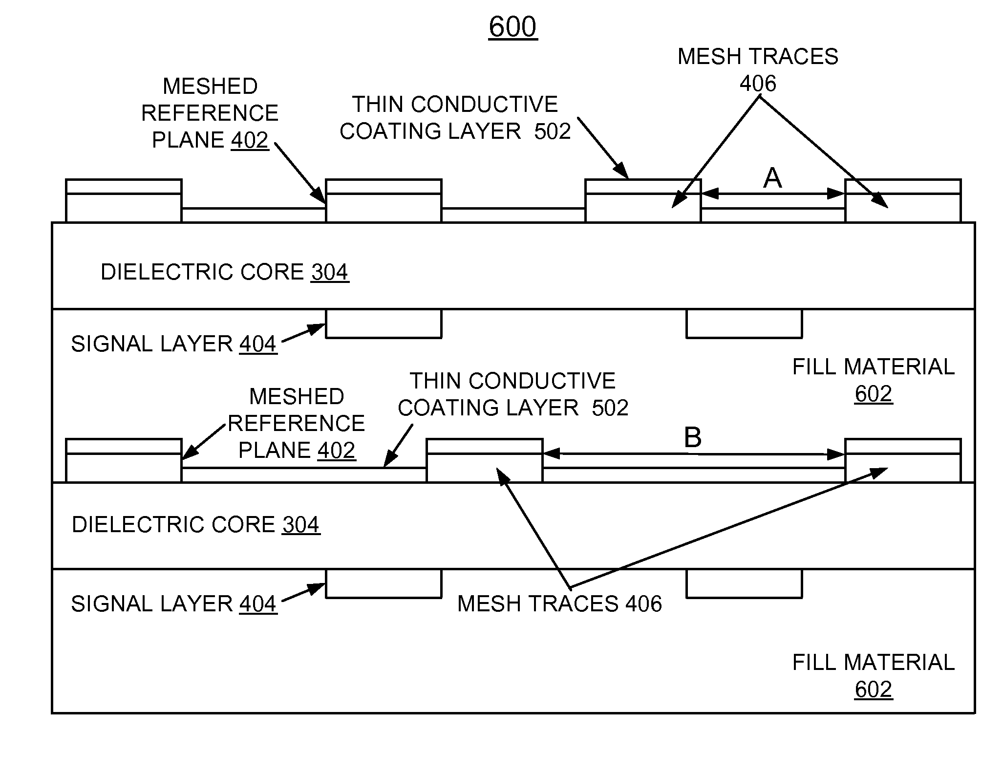
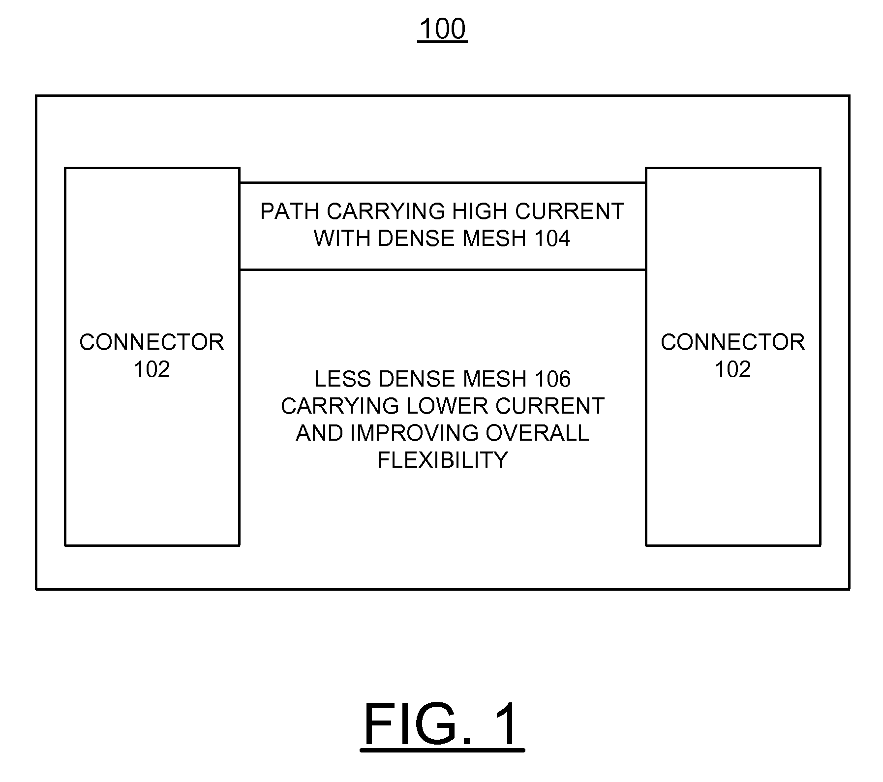
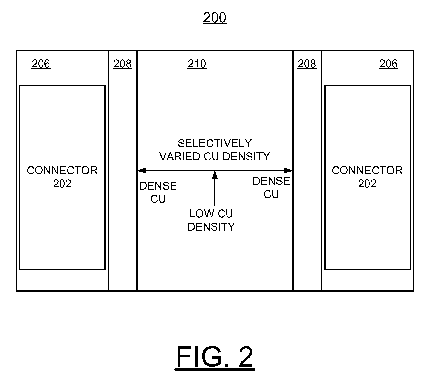
- A method and structure implementing a variable pitch meshed reference plane with a thin copper coating, separated by a dielectric core, allowing for enhanced mechanical flexibility and constant signal impedance by using a dense mesh for high current areas and a less dense mesh for low current areas, with the copper coating deposited via sputtering to maintain flexibility.

Wafer backing member for mechanical and chemical-mechanical planarization of substrates
PatentInactiveUS5830806A
Innovation
- A wafer backing member with a rigid first layer to inhibit wafer flexing and a compressible second layer to cushion the wafer, reducing pressure differences and enabling uniform force distribution, made from materials like epoxy fiberglass or PTFE for the first layer and resilient foam or porous materials for the second layer.


Thermal Management Considerations in Flexible Packaging
Thermal management represents a critical design consideration when evaluating mechanical flexibility approaches in advanced packaging technologies. The fundamental difference between wafer reconstitution and embedding methodologies creates distinct thermal challenges that directly impact the viability of flexible packaging solutions.
In wafer reconstitution processes, the thermal pathway typically involves multiple material interfaces, including the reconstituted substrate, adhesive layers, and the redistributed interconnect structures. The coefficient of thermal expansion (CTE) mismatch between these heterogeneous materials becomes particularly pronounced under thermal cycling conditions. This mismatch generates thermomechanical stress that can compromise the mechanical flexibility advantages initially sought through reconstitution approaches.
Embedding technologies present alternative thermal management characteristics due to their monolithic integration approach. The embedded components experience more uniform thermal distribution through the host substrate material, reducing localized hot spots that could degrade flexible packaging performance. However, the thermal conductivity limitations of typical embedding materials, such as organic substrates, can create challenges in dissipating heat generated by high-power density components.
The thermal interface resistance between different material layers significantly influences the overall thermal performance in both approaches. Reconstituted structures often exhibit higher thermal interface resistance due to multiple bonding interfaces, while embedded solutions may achieve lower resistance through direct material integration. This difference becomes critical when considering the thermal budget constraints of flexible packaging applications.
Package-level thermal simulation results indicate that embedding approaches generally provide more predictable thermal behavior under mechanical deformation conditions. The integrated thermal pathway remains more stable during bending or twisting operations compared to reconstituted structures, where interface delamination risks increase under combined thermal and mechanical stress conditions.
Advanced thermal management solutions, including integrated heat spreaders and thermal via structures, show different implementation complexities between the two approaches. Reconstitution processes offer greater flexibility in incorporating dedicated thermal management features, while embedding methods require more sophisticated design optimization to achieve equivalent thermal performance without compromising mechanical flexibility objectives.
In wafer reconstitution processes, the thermal pathway typically involves multiple material interfaces, including the reconstituted substrate, adhesive layers, and the redistributed interconnect structures. The coefficient of thermal expansion (CTE) mismatch between these heterogeneous materials becomes particularly pronounced under thermal cycling conditions. This mismatch generates thermomechanical stress that can compromise the mechanical flexibility advantages initially sought through reconstitution approaches.
Embedding technologies present alternative thermal management characteristics due to their monolithic integration approach. The embedded components experience more uniform thermal distribution through the host substrate material, reducing localized hot spots that could degrade flexible packaging performance. However, the thermal conductivity limitations of typical embedding materials, such as organic substrates, can create challenges in dissipating heat generated by high-power density components.
The thermal interface resistance between different material layers significantly influences the overall thermal performance in both approaches. Reconstituted structures often exhibit higher thermal interface resistance due to multiple bonding interfaces, while embedded solutions may achieve lower resistance through direct material integration. This difference becomes critical when considering the thermal budget constraints of flexible packaging applications.
Package-level thermal simulation results indicate that embedding approaches generally provide more predictable thermal behavior under mechanical deformation conditions. The integrated thermal pathway remains more stable during bending or twisting operations compared to reconstituted structures, where interface delamination risks increase under combined thermal and mechanical stress conditions.
Advanced thermal management solutions, including integrated heat spreaders and thermal via structures, show different implementation complexities between the two approaches. Reconstitution processes offer greater flexibility in incorporating dedicated thermal management features, while embedding methods require more sophisticated design optimization to achieve equivalent thermal performance without compromising mechanical flexibility objectives.
Reliability Testing Standards for Flexible Wafer Solutions
The establishment of comprehensive reliability testing standards for flexible wafer solutions represents a critical framework for evaluating the long-term performance and durability of both wafer reconstitution and embedding technologies. These standards must address the unique mechanical challenges posed by flexible substrates while ensuring consistent evaluation methodologies across different implementation approaches.
Current industry standards primarily focus on rigid semiconductor packaging, creating a significant gap in testing protocols for flexible applications. The development of specialized testing standards requires consideration of multiple stress factors including cyclic bending, torsional loading, temperature cycling under mechanical stress, and humidity exposure combined with flexural deformation. These multi-modal stress conditions better simulate real-world operating environments where flexible electronic devices experience simultaneous thermal and mechanical loading.
Mechanical flexibility testing protocols must incorporate standardized bend radius specifications, typically ranging from 1mm to 50mm depending on application requirements. The testing methodology should define specific bend angles, cycling frequencies, and total cycle counts that reflect anticipated service life conditions. For wafer reconstitution approaches, particular attention must be paid to die-to-die interconnect integrity under flexural stress, while embedding solutions require focused evaluation of substrate-embedded component interface reliability.
Temperature cycling standards for flexible solutions differ significantly from conventional reliability testing due to the coefficient of thermal expansion mismatches between flexible substrates and embedded components. Testing protocols should specify temperature ranges from -40°C to +125°C with controlled ramp rates to prevent thermal shock while maintaining mechanical flexing during thermal transitions.
Accelerated aging methodologies specific to flexible wafer technologies must account for the synergistic effects of environmental exposure and mechanical stress. Combined temperature-humidity-bias testing under continuous or intermittent flexural loading provides more realistic reliability projections than individual stress testing approaches.
Standardized failure criteria definition remains crucial for meaningful reliability assessment. These criteria should encompass electrical parameter drift, mechanical fracture detection, delamination onset, and functional performance degradation thresholds. The integration of real-time monitoring capabilities during testing enables precise failure mode identification and reliability model validation.
Current industry standards primarily focus on rigid semiconductor packaging, creating a significant gap in testing protocols for flexible applications. The development of specialized testing standards requires consideration of multiple stress factors including cyclic bending, torsional loading, temperature cycling under mechanical stress, and humidity exposure combined with flexural deformation. These multi-modal stress conditions better simulate real-world operating environments where flexible electronic devices experience simultaneous thermal and mechanical loading.
Mechanical flexibility testing protocols must incorporate standardized bend radius specifications, typically ranging from 1mm to 50mm depending on application requirements. The testing methodology should define specific bend angles, cycling frequencies, and total cycle counts that reflect anticipated service life conditions. For wafer reconstitution approaches, particular attention must be paid to die-to-die interconnect integrity under flexural stress, while embedding solutions require focused evaluation of substrate-embedded component interface reliability.
Temperature cycling standards for flexible solutions differ significantly from conventional reliability testing due to the coefficient of thermal expansion mismatches between flexible substrates and embedded components. Testing protocols should specify temperature ranges from -40°C to +125°C with controlled ramp rates to prevent thermal shock while maintaining mechanical flexing during thermal transitions.
Accelerated aging methodologies specific to flexible wafer technologies must account for the synergistic effects of environmental exposure and mechanical stress. Combined temperature-humidity-bias testing under continuous or intermittent flexural loading provides more realistic reliability projections than individual stress testing approaches.
Standardized failure criteria definition remains crucial for meaningful reliability assessment. These criteria should encompass electrical parameter drift, mechanical fracture detection, delamination onset, and functional performance degradation thresholds. The integration of real-time monitoring capabilities during testing enables precise failure mode identification and reliability model validation.
Unlock deeper insights with PatSnap Eureka Quick Research — get a full tech report to explore trends and direct your research. Try now!
Generate Your Research Report Instantly with AI Agent
Supercharge your innovation with PatSnap Eureka AI Agent Platform!