Compare MOSFET Gate Drivers for Robust Switching Control
APR 1, 20269 MIN READ
Generate Your Research Report Instantly with AI Agent
Patsnap Eureka helps you evaluate technical feasibility & market potential.
MOSFET Gate Driver Technology Background and Objectives
MOSFET gate drivers have emerged as critical components in modern power electronics systems, serving as the essential interface between low-power control circuits and high-power switching devices. These specialized circuits amplify control signals from microcontrollers or digital signal processors to provide sufficient current and voltage levels required to rapidly switch MOSFETs between their on and off states. The fundamental role of gate drivers extends beyond simple signal amplification, encompassing critical functions such as electrical isolation, noise immunity, and protection against fault conditions.
The evolution of MOSFET gate driver technology has been driven by the increasing demands of power electronics applications across multiple industries. From automotive electric vehicle inverters to renewable energy systems, industrial motor drives, and high-frequency switching power supplies, the need for robust switching control has become paramount. Modern applications require gate drivers capable of operating at switching frequencies exceeding several hundred kilohertz while maintaining precise timing control and minimizing switching losses.
Contemporary gate driver designs must address several fundamental challenges inherent in high-power switching applications. These include managing high dv/dt transients that can cause false triggering, providing adequate drive strength for large power MOSFETs with significant gate capacitance, and maintaining stable operation across wide temperature ranges. Additionally, electromagnetic interference mitigation and common-mode transient immunity have become increasingly critical as power density requirements continue to escalate.
The primary objective of advancing MOSFET gate driver technology centers on achieving optimal balance between switching speed, efficiency, and reliability. Fast switching transitions minimize conduction and switching losses, directly impacting overall system efficiency. However, excessively rapid switching can generate electromagnetic interference and stress system components. Therefore, gate drivers must provide controllable switching characteristics while maintaining robust operation under adverse conditions.
Protection functionality represents another crucial objective in gate driver development. Advanced gate drivers incorporate features such as undervoltage lockout, overcurrent protection, and desaturation detection to safeguard both the driver circuit and the power MOSFET from potentially destructive fault conditions. These protection mechanisms must respond rapidly enough to prevent device damage while avoiding false triggering during normal operation.
The integration of intelligent features into gate driver designs has become an increasingly important objective. Modern gate drivers often include programmable drive strength, adaptive dead-time control, and diagnostic capabilities that enable real-time monitoring of switching performance. These features support the development of more sophisticated power management systems capable of optimizing performance dynamically based on operating conditions.
Market Demand for Robust MOSFET Switching Solutions
The global power electronics market is experiencing unprecedented growth driven by the accelerating adoption of electric vehicles, renewable energy systems, and advanced industrial automation. This expansion has created substantial demand for robust MOSFET switching solutions that can deliver superior performance, reliability, and efficiency across diverse applications. The automotive sector represents one of the most significant growth drivers, with electric vehicle manufacturers requiring gate drivers capable of handling high-frequency switching operations while maintaining thermal stability and electromagnetic compatibility.
Industrial automation and motor control applications constitute another major demand segment, where precise switching control directly impacts system efficiency and operational reliability. Manufacturing facilities increasingly require gate drivers that can operate reliably in harsh industrial environments while providing consistent performance across varying load conditions. The trend toward higher power density and miniaturization in industrial equipment has intensified the need for compact yet robust switching solutions.
Renewable energy infrastructure development has generated substantial market opportunities for advanced MOSFET gate drivers. Solar inverters and wind power conversion systems demand switching solutions capable of handling high-voltage operations with minimal power losses. Grid-tied applications particularly require gate drivers with exceptional noise immunity and fault protection capabilities to ensure stable power delivery and grid compliance.
The telecommunications and data center sectors represent rapidly expanding markets for robust switching solutions. The proliferation of cloud computing and edge computing infrastructure has created demand for highly efficient power management systems. Data centers require gate drivers that can maintain consistent performance while minimizing power consumption and heat generation, directly impacting operational costs and environmental sustainability.
Consumer electronics manufacturers are increasingly seeking compact, cost-effective gate driver solutions that can support fast charging technologies and wireless power transfer systems. The integration of power management functions into portable devices has created demand for switching solutions that combine high efficiency with minimal electromagnetic interference.
Market dynamics indicate strong preference for gate drivers offering integrated protection features, including overcurrent detection, thermal shutdown, and shoot-through prevention. End users prioritize solutions that reduce system complexity while enhancing reliability and safety margins across operating conditions.
Current State and Challenges in Gate Driver Technology
MOSFET gate driver technology has evolved significantly over the past decade, with current implementations spanning from discrete solutions to highly integrated systems-on-chip. Modern gate drivers primarily utilize silicon-based architectures, though silicon carbide and gallium nitride variants are gaining traction in high-frequency applications. The technology landscape is dominated by isolated and non-isolated driver configurations, each serving distinct application requirements in power electronics systems.
Contemporary gate driver designs face substantial challenges in achieving optimal switching performance while maintaining system reliability. Propagation delay variations remain a critical concern, particularly in high-frequency switching applications where nanosecond-level timing precision directly impacts efficiency and electromagnetic interference characteristics. Current solutions struggle to maintain consistent delay times across temperature variations and manufacturing tolerances, leading to suboptimal switching synchronization in multi-phase power systems.
Power delivery to gate drivers presents another significant technical hurdle. Existing bootstrap circuits and isolated power supplies often exhibit limitations in continuous high-side operation, particularly during extended low-side off periods. This constraint becomes more pronounced in applications requiring high duty cycles or low-frequency operation, where charge pump depletion can compromise switching reliability and introduce unwanted delays.
Thermal management challenges persist across current gate driver implementations. High-power switching applications generate substantial heat within driver circuits, affecting both performance consistency and long-term reliability. Existing thermal mitigation strategies, including advanced packaging and heat spreading techniques, add complexity and cost while providing only incremental improvements in thermal performance.
Protection mechanisms in current gate drivers demonstrate varying degrees of sophistication and effectiveness. While basic overcurrent and undervoltage lockout features are standard, advanced protection schemes for short-circuit detection and active gate clamping remain inconsistent across different manufacturer implementations. This variability creates integration challenges for system designers seeking robust fault protection.
The integration density of modern gate drivers continues to increase, yet this advancement introduces new challenges in signal integrity and crosstalk mitigation. High-density packaging often compromises isolation performance and increases susceptibility to electromagnetic interference, requiring careful design trade-offs between functionality and reliability.
Current gate driver technology also faces limitations in adaptive control capabilities. Most existing solutions operate with fixed parameters, lacking the intelligence to dynamically adjust switching characteristics based on real-time operating conditions, load variations, or aging effects, which limits their effectiveness in optimizing system performance across diverse operating scenarios.
Existing Gate Driver Solutions for Switching Control
01 Gate driver circuits with adaptive timing control
MOSFET gate drivers can incorporate adaptive timing control mechanisms to optimize switching performance. These circuits adjust the gate drive timing based on operating conditions such as load current, temperature, or voltage levels. The adaptive control helps minimize switching losses and electromagnetic interference while maintaining reliable operation. Advanced implementations may include feedback loops that monitor switching transitions and dynamically adjust drive strength and timing parameters.- Gate driver circuits with adaptive timing control: MOSFET gate drivers can incorporate adaptive timing control mechanisms to optimize switching performance. These circuits adjust the gate drive timing based on operating conditions such as load current, temperature, or voltage levels. The adaptive control helps minimize switching losses and electromagnetic interference while maintaining reliable operation. Advanced implementations may include feedback loops that monitor the MOSFET switching behavior and dynamically adjust drive parameters to achieve optimal performance across varying operating conditions.
- Multi-level gate drive voltage control: Gate driver designs can utilize multi-level voltage control strategies to improve switching characteristics. These approaches apply different voltage levels during turn-on and turn-off transitions to control the switching speed and reduce voltage and current stresses. The technique may involve applying a higher initial voltage for fast turn-on, followed by a lower sustaining voltage, or using intermediate voltage levels during transitions. This method helps balance switching speed with electromagnetic compatibility requirements and reduces device stress.
- Active gate drive with current source control: Active gate driver circuits employ current source control to precisely manage the charging and discharging of the MOSFET gate capacitance. By controlling the gate current rather than simply applying voltage, these drivers can achieve more predictable and controllable switching transitions. This approach allows for independent control of turn-on and turn-off speeds, enabling optimization of switching losses and electromagnetic interference. The current source control can be implemented with adjustable current levels to accommodate different operating conditions and MOSFET characteristics.
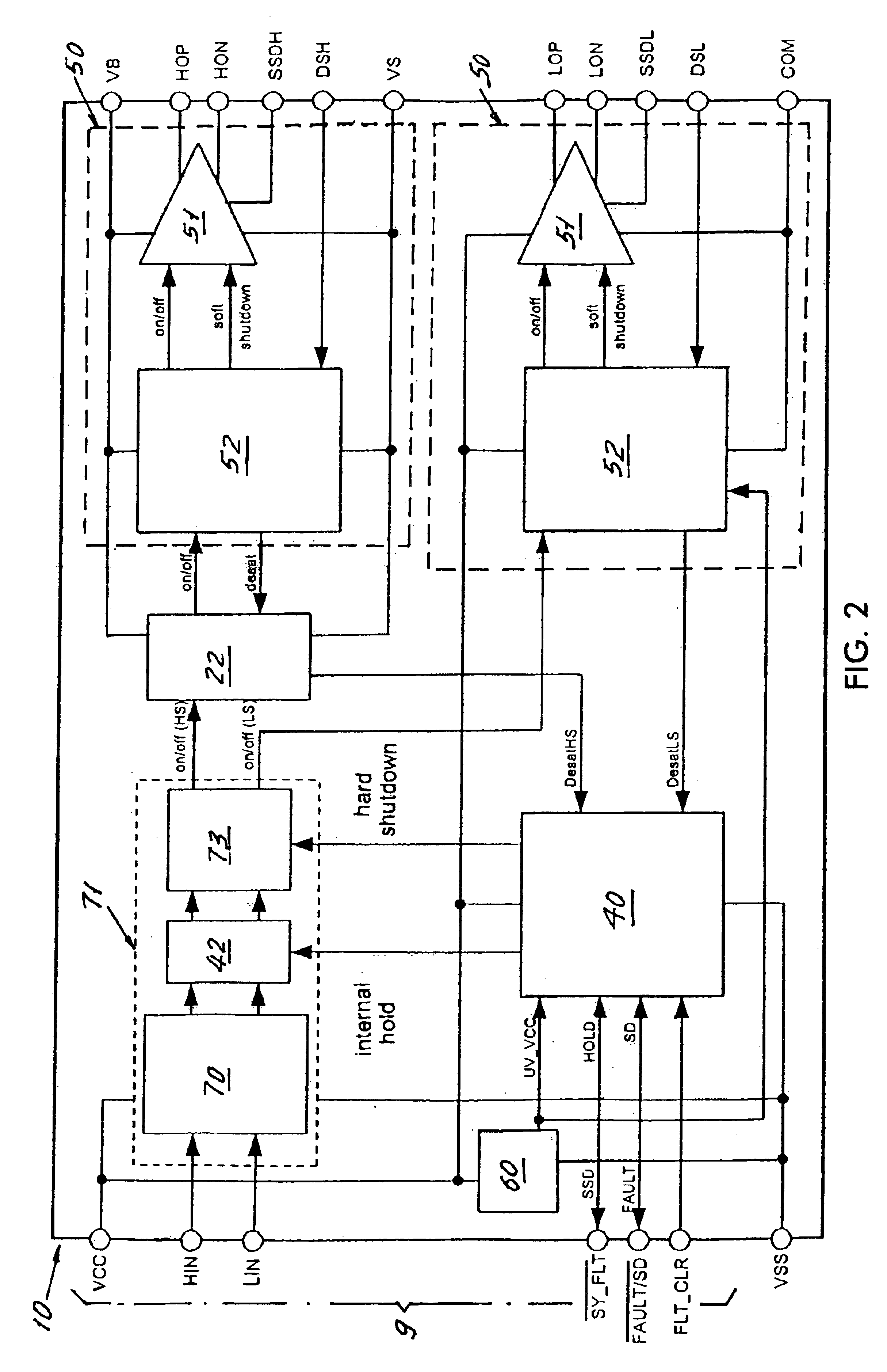
- Gate driver protection and fault detection: MOSFET gate driver circuits incorporate protection mechanisms and fault detection capabilities to ensure safe operation. These features include overcurrent detection, short-circuit protection, and desaturation monitoring that can detect fault conditions and quickly disable the gate drive signal. Additional protection functions may include under-voltage lockout, thermal shutdown, and gate-source voltage clamping. The protection circuits work in conjunction with control logic to prevent device damage and system failures while providing diagnostic information for fault analysis.
- Isolated gate driver with high-speed signal transmission: Isolated gate driver designs provide galvanic isolation between control and power circuits while maintaining high-speed signal transmission capabilities. These drivers use isolation techniques such as optical, magnetic, or capacitive coupling to transfer gate control signals across the isolation barrier. The isolation protects low-voltage control circuits from high-voltage transients and enables proper operation in applications with floating or high-side switches. Advanced implementations focus on minimizing propagation delay and maintaining signal integrity across the isolation barrier to preserve precise switching control.
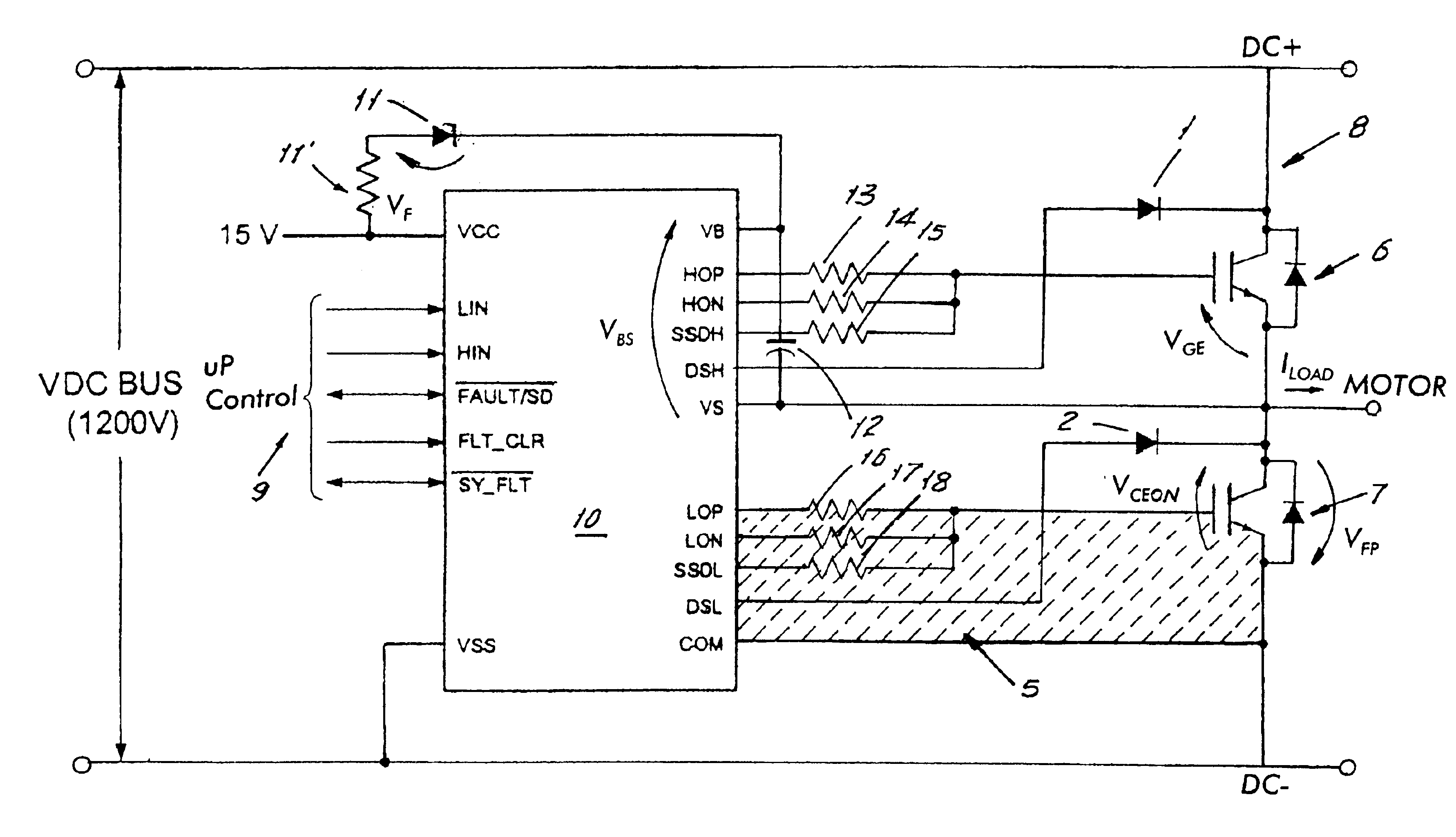
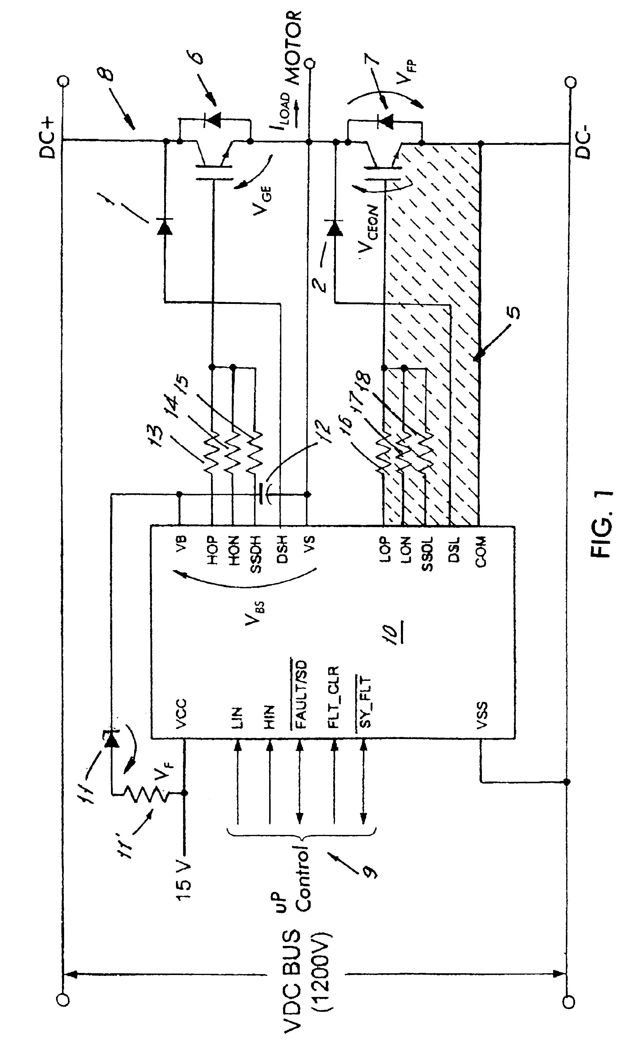
02 Bootstrap and charge pump circuits for high-side gate driving
High-side MOSFET gate drivers require voltage level shifting techniques to provide adequate gate voltage above the source terminal. Bootstrap circuits using capacitors and diodes, or charge pump configurations, generate the necessary floating supply voltage. These circuits enable efficient driving of high-side switches in half-bridge and full-bridge topologies. Design considerations include bootstrap capacitor sizing, refresh timing, and prevention of undervoltage conditions during extended on-times.Expand Specific Solutions03 Dead-time control and shoot-through prevention
Gate driver circuits implement dead-time control to prevent simultaneous conduction of complementary MOSFETs in bridge configurations. This involves introducing controlled delays between turn-off of one switch and turn-on of the complementary switch. Advanced techniques include adaptive dead-time adjustment based on load conditions and temperature compensation. Some implementations incorporate shoot-through detection and protection mechanisms that monitor drain-source voltages and can disable gate signals if abnormal conditions are detected.Expand Specific Solutions04 Gate drive strength and slew rate control
Controlling the gate drive strength and voltage slew rate is essential for managing switching speed, electromagnetic interference, and voltage/current stress. Gate drivers may incorporate adjustable output impedance, multi-stage drive circuits, or active gate control to shape the switching transitions. Techniques include using series gate resistors, parallel drive stages that activate sequentially, or feedback-controlled current sources. These methods allow optimization of the trade-off between switching losses and electromagnetic compatibility.Expand Specific Solutions05 Integrated protection and diagnostic features
Modern MOSFET gate drivers integrate various protection and diagnostic capabilities to enhance system reliability. These include overcurrent detection, overtemperature monitoring, undervoltage lockout, and fault reporting mechanisms. Some implementations provide desaturation detection to identify MOSFET failures or short-circuit conditions. Diagnostic features may include status outputs, current sensing, and communication interfaces that enable real-time monitoring of switching performance and early detection of degradation or fault conditions.Expand Specific Solutions
Key Players in Gate Driver IC Industry
The MOSFET gate driver market is experiencing robust growth driven by increasing demand for efficient power management across automotive, industrial automation, and renewable energy sectors. The industry has reached a mature development stage with established players like Infineon Technologies, ON Semiconductor, Monolithic Power Systems, and Toshiba leading technological advancement. Market expansion is fueled by electric vehicle adoption and industrial digitalization trends. Technology maturity varies significantly among competitors - Infineon and ON Semiconductor demonstrate high sophistication in integrated solutions, while companies like SolarEdge and Mitsubishi Electric focus on specialized applications. Emerging players such as Global Power Technology and ETA Green Power are introducing innovative approaches with SiC-based solutions. The competitive landscape shows consolidation among tier-one suppliers, with differentiation occurring through advanced packaging, integration levels, and application-specific optimizations for switching performance and reliability.
Semiconductor Components Industries LLC
Technical Solution: ON Semiconductor provides robust MOSFET gate drivers with focus on automotive and industrial applications. Their NCV series drivers offer enhanced EMI performance and functional safety compliance with ASIL-D ratings. The drivers feature adaptive dead-time control, programmable slew rate adjustment, and integrated bootstrap diodes for high-side switching. With output drive currents ranging from 1.5A to 9A and operating temperatures up to 150°C, these solutions ensure reliable switching performance in harsh environments while minimizing switching losses through optimized gate charge control.
Strengths: Automotive-grade reliability, functional safety compliance, adaptive control features. Weaknesses: Limited high-frequency performance, smaller product range compared to competitors.
Monolithic Power Systems, Inc.
Technical Solution: MPS delivers high-performance MOSFET gate drivers with proprietary BCD technology enabling compact integration and superior switching characteristics. Their drivers feature ultra-fast propagation delays under 25ns and high peak output currents exceeding 10A for rapid MOSFET switching. The solutions incorporate advanced level-shifting techniques for high-voltage applications up to 600V with excellent dv/dt immunity exceeding 100V/ns. MPS drivers also include intelligent protection features such as undervoltage lockout, thermal shutdown, and shoot-through prevention to ensure robust operation in demanding power conversion applications.
Strengths: Ultra-fast switching speeds, compact integration, excellent dv/dt immunity. Weaknesses: Limited isolation options, higher power consumption in some applications.
Core Innovations in Robust Gate Driver Design
Gate driver and switching apparatus
PatentPendingEP4672608A1
Innovation
- A gate driver circuit with a controllable capacitor circuit that provides adjustable external gate capacitance in parallel with the internal capacitance, allowing selective control of external gate capacitance values through controllable capacitor legs, enabling flexible adjustment of switching characteristics.


Half-bridge high voltage gate driver providing protection of a transistor
PatentInactiveUS6859087B2
Innovation
- A gate driver integrated circuit with an external supply voltage and controller, featuring an output stage for soft shutdown, fault control circuit for prioritizing desaturation protection, and bootstrap supply techniques, enabling low quiescent current operation and reducing electromagnetic emissions without a floating power supply.

EMI Compliance Standards for Gate Driver Applications
Electromagnetic interference (EMI) compliance represents a critical regulatory framework that MOSFET gate driver applications must satisfy to ensure reliable operation in diverse electronic environments. The primary standards governing EMI emissions include CISPR 25 for automotive applications, FCC Part 15 for commercial electronics, and IEC 61000 series for industrial equipment. These regulations establish stringent limits on both conducted and radiated emissions across frequency ranges from 150 kHz to several GHz.
Gate driver circuits inherently generate high-frequency switching noise due to rapid voltage transitions and current changes during MOSFET switching operations. The fast rise and fall times, typically in the nanosecond range, create broadband spectral content that can violate EMI limits without proper design considerations. Critical emission sources include gate drive loops, power switching nodes, and parasitic coupling paths between high-speed digital circuits and sensitive analog components.
Conducted emissions primarily propagate through power supply lines and ground connections, requiring careful attention to power delivery network design and filtering strategies. Common-mode and differential-mode noise characteristics differ significantly, necessitating tailored suppression approaches. Ferrite beads, common-mode chokes, and ceramic capacitors form the foundation of conducted EMI mitigation, with placement and component selection directly impacting compliance margins.
Radiated emissions emerge from current loops formed by gate driver circuits, PCB traces, and component packaging. Minimizing loop areas through strategic component placement and ground plane optimization significantly reduces far-field radiation. Shielding techniques, including metal enclosures and conductive gaskets, provide additional attenuation for sensitive applications where design-level mitigation proves insufficient.
Testing methodologies specified in EMI standards require specialized equipment including EMI receivers, line impedance stabilization networks (LISN), and anechoic chambers for radiated measurements. Pre-compliance testing using near-field probes and spectrum analyzers enables early identification of potential violations during development phases, reducing certification risks and associated costs.
Automotive applications face particularly stringent requirements under CISPR 25, with Class 5 limits demanding exceptional noise control for safety-critical systems. Industrial gate driver applications must comply with IEC 61000-6-4 emission standards while maintaining immunity to external interference sources as defined in IEC 61000-6-2.
Thermal Management Considerations in Gate Driver Design
Thermal management represents a critical design consideration in MOSFET gate driver circuits, directly impacting switching performance, reliability, and overall system robustness. Gate drivers inherently generate heat through various mechanisms including quiescent power consumption, switching losses during charge and discharge cycles, and resistive losses in output stages. Effective thermal design becomes increasingly important as switching frequencies rise and power densities increase in modern power electronics applications.
The primary heat sources in gate driver circuits stem from the output buffer stages that must rapidly charge and discharge MOSFET gate capacitances. During each switching transition, energy stored in gate capacitance is dissipated as heat within the driver's output transistors. This power dissipation scales with switching frequency and gate charge requirements, making thermal considerations paramount in high-frequency applications. Additionally, shoot-through currents in complementary output stages and quiescent bias currents contribute to steady-state power consumption.
Package selection significantly influences thermal performance, with considerations extending beyond basic thermal resistance values. Modern gate driver packages incorporate exposed thermal pads, multiple ground connections, and optimized lead frame designs to enhance heat dissipation. Advanced packaging technologies such as flip-chip and wafer-level chip-scale packages offer superior thermal characteristics compared to traditional plastic packages, enabling higher power density implementations.
Junction temperature management directly affects switching characteristics and long-term reliability. Elevated temperatures increase propagation delays, reduce noise margins, and can lead to thermal runaway conditions in poorly designed systems. Temperature-dependent parameters such as threshold voltages and transconductance variations must be considered during driver selection to maintain consistent switching performance across operating temperature ranges.
Thermal design strategies encompass both component-level and system-level approaches. At the component level, selecting drivers with lower thermal resistance and higher temperature ratings provides immediate benefits. System-level considerations include PCB thermal design with appropriate copper areas, thermal vias, and heat spreading techniques. Advanced implementations may incorporate active cooling solutions or temperature monitoring with adaptive control algorithms.
Modern gate drivers increasingly integrate thermal protection features including over-temperature shutdown, thermal monitoring outputs, and temperature-compensated timing circuits. These features enhance system robustness by preventing thermal damage while maintaining optimal performance across varying operating conditions, making thermal-aware driver selection essential for reliable switching control implementations.
Unlock deeper insights with Patsnap Eureka Quick Research — get a full tech report to explore trends and direct your research. Try now!
Generate Your Research Report Instantly with AI Agent
Supercharge your innovation with Patsnap Eureka AI Agent Platform!