Compare Multi Chip Module vs Advanced Packaging for Lightness
MAR 12, 20269 MIN READ
Generate Your Research Report Instantly with AI Agent
PatSnap Eureka helps you evaluate technical feasibility & market potential.
MCM vs Advanced Packaging Lightness Goals
The pursuit of lightweight electronic systems has become a critical driver in modern technology development, particularly in aerospace, automotive, and portable consumer electronics applications. Both Multi Chip Module (MCM) and Advanced Packaging technologies have emerged as viable solutions to address weight reduction challenges while maintaining or enhancing performance capabilities. The fundamental objective centers on achieving optimal power-to-weight ratios and functional density without compromising reliability or thermal management.
MCM technology primarily targets lightness through substrate material optimization and three-dimensional integration approaches. The core lightness goals include reducing overall package thickness by 30-50% compared to traditional discrete component assemblies, minimizing interconnect materials through shorter trace lengths, and eliminating redundant packaging layers. Silicon-based MCM substrates typically achieve weight reductions of 15-25% while ceramic substrates can deliver up to 40% weight savings through material density advantages.
Advanced Packaging solutions pursue lightness objectives through innovative structural designs and material engineering. Key goals encompass achieving ultra-thin form factors below 0.5mm thickness, implementing wafer-level packaging to eliminate traditional package substrates, and utilizing advanced polymer materials with densities 60-70% lower than conventional ceramic substrates. Fan-out wafer-level packaging (FOWLP) specifically targets weight reductions exceeding 50% while maintaining electrical performance standards.
The comparative lightness objectives reveal distinct strategic approaches. MCM focuses on system-level weight optimization through component consolidation and substrate efficiency, typically achieving 20-35% weight reductions in complete assemblies. Advanced Packaging emphasizes individual component lightness through material innovation and structural miniaturization, often delivering 40-60% weight savings at the package level.
Both technologies share common lightness goals including thermal management efficiency without additional cooling hardware, mechanical robustness despite reduced material usage, and scalability across different application requirements. The ultimate objective involves balancing weight reduction with manufacturing feasibility, cost considerations, and long-term reliability performance in demanding operational environments.
Market Demand for Lightweight Electronic Packaging
The global electronics industry is experiencing unprecedented demand for lightweight packaging solutions, driven by the convergence of multiple technological trends and consumer expectations. Mobile device manufacturers face intense pressure to deliver thinner, lighter products while maintaining or enhancing performance capabilities. This demand extends beyond smartphones to include tablets, laptops, wearables, and emerging form factors where weight reduction directly impacts user experience and market competitiveness.
Automotive electronics represents another significant growth driver for lightweight packaging technologies. As vehicles transition toward electrification and autonomous driving capabilities, the proliferation of electronic control units, sensors, and computing modules creates substantial weight challenges. Every gram saved in electronic packaging contributes to improved fuel efficiency, extended battery range, and enhanced vehicle performance. The automotive sector's stringent reliability requirements further intensify the need for advanced packaging solutions that can deliver both weight reduction and robust performance under harsh operating conditions.
The aerospace and defense industries continue to be early adopters and key demand drivers for lightweight electronic packaging. Aircraft manufacturers require electronic systems that minimize weight penalties while meeting rigorous safety and performance standards. Satellite applications demand packaging solutions that can withstand extreme environmental conditions while maintaining minimal mass to reduce launch costs. These high-value applications often justify premium pricing for advanced packaging technologies, creating attractive market opportunities for innovative solutions.
Consumer electronics market dynamics increasingly favor products that combine powerful functionality with portability. The rise of edge computing, artificial intelligence processing, and high-resolution displays in portable devices creates complex packaging challenges. Manufacturers must integrate more functionality into smaller, lighter packages while managing thermal dissipation and maintaining signal integrity. This trend drives continuous innovation in both multi-chip module architectures and advanced packaging techniques.
Industrial Internet of Things applications generate substantial demand for lightweight, compact electronic modules that can be deployed in diverse environments. These applications often require ruggedized packaging that maintains low weight profiles while providing reliable operation across extended temperature ranges and challenging environmental conditions. The scalability requirements of IoT deployments make cost-effective lightweight packaging solutions particularly valuable in this market segment.
Healthcare and medical device markets increasingly demand portable, wearable electronic systems that minimize patient burden while delivering sophisticated monitoring and treatment capabilities. Lightweight packaging becomes critical for patient comfort and device adoption, particularly in applications requiring extended wear periods or implantable configurations.
Current State of MCM and Advanced Packaging Technologies
Multi Chip Module (MCM) technology has evolved significantly since its inception in the 1980s, transitioning from ceramic-based substrates to sophisticated silicon interposers and organic substrates. Current MCM implementations utilize high-density interconnects with pitch sizes ranging from 10-50 micrometers, enabling multiple dies to be integrated within a single package. Leading MCM solutions achieve interconnect densities exceeding 10,000 I/Os per square centimeter while maintaining thermal management capabilities through advanced heat dissipation structures.
Advanced packaging technologies have diversified into multiple architectural approaches, each addressing specific performance and form factor requirements. Through-Silicon Via (TSV) technology enables vertical stacking with via diameters as small as 5 micrometers, facilitating 3D integration with reduced footprint. Fan-out wafer-level packaging (FOWLP) has emerged as a dominant solution, offering redistribution layer capabilities that extend I/O connections beyond the die boundaries while maintaining package thickness below 0.5mm.
System-in-Package (SiP) architectures represent the current pinnacle of advanced packaging, integrating heterogeneous components including processors, memory, passive elements, and RF modules within unified packages. Contemporary SiP solutions achieve component integration densities that reduce overall system volume by 40-60% compared to traditional discrete component assemblies. These packages incorporate embedded components within substrate layers, further optimizing space utilization.
Wafer-level chip-scale packaging (WLCSP) has matured to support die sizes up to 20mm while maintaining package thickness ratios below 1.2 times the die thickness. Current WLCSP implementations utilize redistribution layers with line widths approaching 2 micrometers, enabling high I/O density while preserving the compact form factor essential for mobile and wearable applications.
Package-on-Package (PoP) stacking technology has advanced to support multi-tier configurations with optimized thermal pathways and signal integrity management. Modern PoP solutions incorporate through-mold vias and cavity-down configurations that minimize package height while maintaining electrical performance standards required for high-frequency applications.
The integration of these packaging technologies with emerging materials, including low-k dielectrics and thermally conductive polymers, has enhanced both electrical performance and thermal management capabilities. Current implementations demonstrate thermal conductivities exceeding 3 W/mK while maintaining dielectric constants below 2.5, enabling lightweight solutions without compromising functionality.
Existing Lightweight Packaging Solutions Comparison
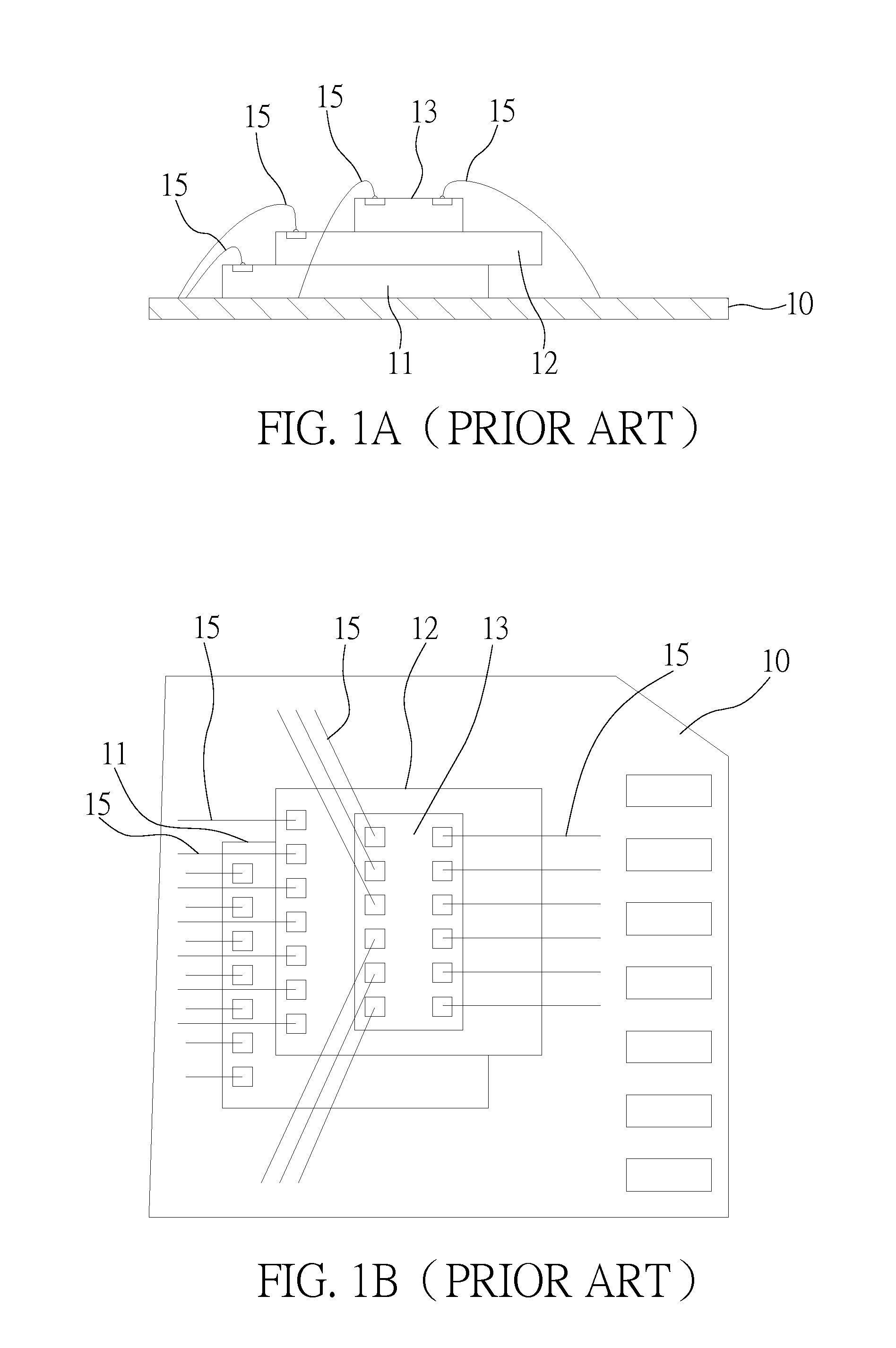
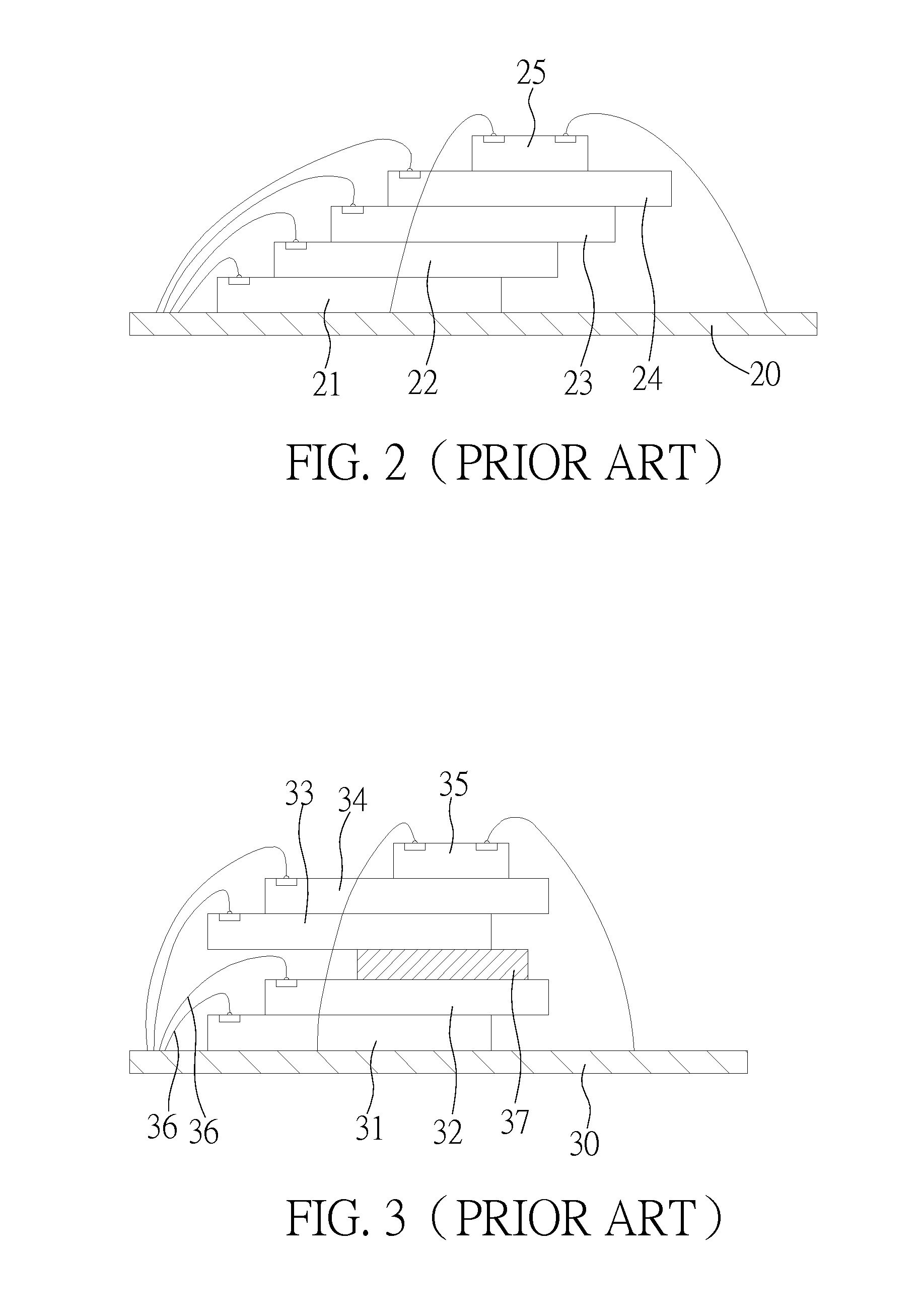
01 Thin substrate and lightweight materials for MCM packaging
Multi-chip modules can achieve lightness through the use of thin substrates and lightweight materials. This approach involves reducing the thickness of the substrate while maintaining structural integrity and electrical performance. Advanced materials such as thin ceramic substrates, flexible polymers, or composite materials can be employed to minimize overall package weight without compromising reliability or thermal management capabilities.- Thin substrate and lightweight materials for MCM packaging: Multi-chip modules can achieve lightness through the use of thin substrates and lightweight materials in the packaging structure. This approach involves reducing the thickness of the substrate while maintaining structural integrity and electrical performance. Advanced materials such as thin laminates, flexible substrates, or composite materials can be employed to minimize overall package weight without compromising functionality or reliability.
- Optimized interconnection structures for weight reduction: Advanced packaging techniques utilize optimized interconnection structures such as through-silicon vias, microbumps, and redistribution layers to reduce the overall package profile and weight. These interconnection methods enable vertical integration and shorter signal paths while eliminating the need for heavy traditional packaging components. The streamlined interconnection architecture contributes to both miniaturization and weight reduction in multi-chip module designs.
- Cavity and hollow structure designs: Implementing cavity structures or hollow regions within the package substrate or encapsulation can significantly reduce the weight of multi-chip modules. These designs strategically remove material from non-critical areas while preserving mechanical strength in load-bearing regions. The cavity approach allows for air gaps or lightweight filler materials to replace denser packaging materials, achieving substantial weight savings in advanced packaging configurations.
- Thin encapsulation and molding compounds: Advanced packaging lightness can be achieved through the application of thin encapsulation layers and lightweight molding compounds. Modern encapsulation materials with improved properties allow for reduced thickness while providing adequate protection against environmental factors and mechanical stress. Low-density molding compounds and thin-film encapsulation techniques minimize the weight contribution from protective layers in multi-chip module packages.
- Integrated heat dissipation with lightweight thermal solutions: Lightweight thermal management solutions integrated into multi-chip module packaging help reduce overall weight while maintaining effective heat dissipation. These solutions include thin heat spreaders, optimized thermal interface materials, and innovative cooling structures that minimize mass. Advanced thermal designs balance the requirements of heat removal with weight constraints, utilizing materials and geometries that maximize thermal performance per unit weight.
02 3D stacking and vertical integration for compact packaging
Three-dimensional stacking techniques enable multiple chips to be vertically integrated, reducing the horizontal footprint and overall package volume. This approach utilizes through-silicon vias and advanced interconnect technologies to create compact, lightweight multi-chip assemblies. The vertical integration allows for shorter interconnect paths, improved performance, and reduced material usage, contributing to overall weight reduction in advanced packaging solutions.Expand Specific Solutions03 Optimized interconnect structures and redistribution layers
Advanced packaging lightness can be achieved through optimized interconnect structures and thin redistribution layers. These designs minimize the amount of conductive and dielectric materials required while maintaining electrical performance. Fine-pitch interconnects, ultra-thin redistribution layers, and innovative bonding techniques reduce the overall thickness and weight of the package assembly. This approach also enables better integration density and improved signal integrity.Expand Specific Solutions04 Cavity and hollow structure designs for weight reduction
Implementing cavity structures and hollow designs within the package substrate or encapsulation can significantly reduce weight while maintaining mechanical strength. These designs strategically remove material from non-critical areas, creating air gaps or hollow sections that decrease overall mass. The approach requires careful structural analysis to ensure adequate support for the chips and protection from environmental factors while achieving substantial weight savings.Expand Specific Solutions05 Advanced molding compounds and thin encapsulation techniques
Lightweight multi-chip modules can be realized through the use of advanced molding compounds with lower density and thin encapsulation techniques. These materials provide adequate protection and mechanical support while minimizing added weight. Thin film encapsulation, compression molding with optimized compound formulations, and selective encapsulation methods reduce the overall package mass. The approach balances protection requirements with weight reduction goals for portable and aerospace applications.Expand Specific Solutions
Key Players in MCM and Advanced Packaging Industry
The Multi Chip Module (MCM) versus Advanced Packaging competition for lightness applications represents a rapidly evolving market in the mature growth stage, driven by increasing demand for compact, lightweight electronic solutions across automotive, mobile, and IoT sectors. The global advanced packaging market, valued at approximately $35 billion, demonstrates strong momentum with major players like Samsung Electronics, TSMC, and Intel leading innovation in 3D packaging and system-in-package technologies. Technology maturity varies significantly, with established companies such as ASE Group, Siliconware Precision Industries, and STATS ChipPAC offering proven MCM solutions, while newer entrants like Onto Innovation and specialized firms including Unimicron Technology push advanced substrate technologies. The competitive landscape shows Asian manufacturers dominating assembly services, while Western companies like Infineon and GlobalFoundries focus on high-performance applications, creating a diverse ecosystem where lightness optimization drives continuous technological advancement.
Samsung Electronics Co., Ltd.
Technical Solution: Samsung has developed I-Cube4 advanced packaging technology that delivers substantial weight reduction compared to traditional Multi Chip Module approaches. Their solution integrates multiple memory and logic dies in a compact vertical stack, achieving up to 35% weight reduction while improving performance density. Samsung's advanced packaging utilizes Through-Silicon-Via (TSV) technology and ultra-thin die stacking, enabling lightweight form factors essential for mobile devices and wearable electronics. The company's packaging solutions focus on heterogeneous integration capabilities, combining different semiconductor technologies in optimized lightweight packages that outperform conventional MCM implementations in weight-sensitive applications.
Strengths: Vertical integration across memory and logic technologies, strong mobile device market presence, proven high-volume manufacturing capabilities. Weaknesses: Limited availability for third-party customers, focus primarily on consumer electronics applications.
Advanced Semiconductor Engineering, Inc.
Technical Solution: ASE Group has developed comprehensive advanced packaging solutions that provide significant weight advantages over traditional Multi Chip Module designs. Their System-in-Package (SiP) technology integrates multiple functional blocks in ultra-compact, lightweight packages, achieving weight reductions of 25-40% compared to equivalent MCM solutions. ASE's advanced packaging portfolio includes fan-out wafer-level packaging (FOWLP) and embedded die technologies that minimize package footprint and weight while maintaining high performance. The company's packaging solutions utilize advanced substrate materials and optimized interconnect designs, enabling lighter form factors for automotive, IoT, and mobile applications where weight constraints are critical design considerations.
Strengths: Comprehensive packaging service capabilities, strong customer relationships across multiple industries, cost-effective manufacturing solutions. Weaknesses: Limited in-house semiconductor design capabilities, dependency on customer-provided die and specifications.
Core Innovations in Ultra-Light Packaging Technologies
Tracking and/or predicting substrate yield during fabrication
PatentWO2024220605A1
Innovation
- A method is introduced to predict the overlay yield of semiconductor lithography processes by measuring attributes of conductive vias before lithography, comparing them to predefined values, and using this data to adjust alignment or scrap batches, while also virtually modeling the substrate to identify potential defects in subsequent layers and optimize the manufacturing process.


Multi-chip stack structure and method for fabricating the same
PatentActiveUS20090140440A1
Innovation
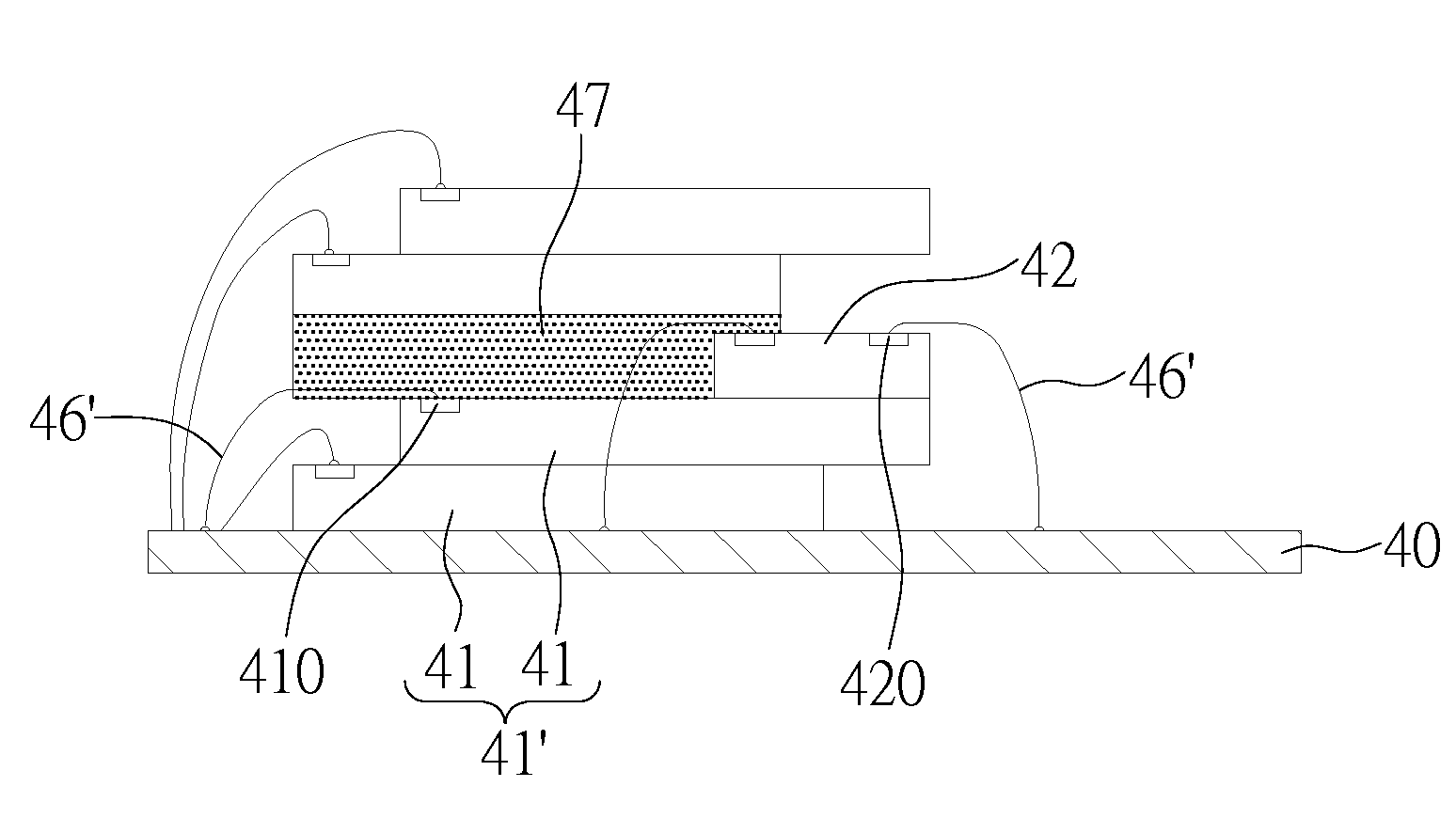
- A method involving a chip carrier with a first chip group stacked in a step-like manner, a second chip connected to the carrier, and a third chip stacked with an insulative film between the first and second chips to prevent bonding wire contact, reducing the need for a buffer layer and simplifying the process, while using a film over wire technique to manage bonding wire ends and reduce arc height.

Material Science Advances for Package Weight Reduction
Material science innovations have emerged as the primary driver for achieving significant weight reduction in both Multi Chip Module (MCM) and advanced packaging technologies. The development of ultra-lightweight substrate materials represents a fundamental breakthrough, with organic substrates incorporating hollow glass microspheres achieving density reductions of up to 40% compared to traditional FR-4 materials while maintaining structural integrity and thermal performance.
Advanced polymer composites utilizing carbon nanotube reinforcement have demonstrated exceptional strength-to-weight ratios, enabling thinner substrate designs without compromising mechanical reliability. These materials exhibit thermal expansion coefficients closely matched to silicon, reducing thermal stress while achieving weight savings of 25-35% in typical packaging applications.
The integration of aerogel-based thermal interface materials has revolutionized heat management approaches in lightweight packaging. These materials provide superior thermal conductivity at densities as low as 0.1 g/cm³, replacing traditional metallic heat spreaders and contributing to overall package weight reduction of 15-20% while improving thermal performance.
Novel metal matrix composites incorporating aluminum-lithium alloys and magnesium-based materials have enabled the development of ultra-lightweight lead frames and interconnect structures. These materials offer density reductions of 30-50% compared to copper-based solutions while maintaining electrical conductivity within acceptable ranges for high-frequency applications.
Breakthrough developments in glass-ceramic substrates with controlled porosity have achieved remarkable weight reduction without sacrificing dielectric properties. These materials utilize precisely engineered microstructures that reduce density by 20-30% while maintaining low dielectric loss and excellent dimensional stability across temperature cycles.
The emergence of bio-inspired hierarchical structures in packaging materials has opened new possibilities for weight optimization. These designs, mimicking natural lightweight structures, achieve superior mechanical properties at reduced material volumes, enabling package weight reductions of 10-25% through optimized material distribution and structural geometry.
Thermal Management in Lightweight Package Design
Thermal management represents one of the most critical challenges in lightweight package design, particularly when comparing Multi Chip Module (MCM) and Advanced Packaging approaches. The fundamental trade-off between weight reduction and heat dissipation efficiency creates complex engineering constraints that significantly influence package architecture decisions.
MCM configurations face unique thermal challenges due to their multi-die arrangement within a single package. The proximity of multiple heat-generating components creates localized hot spots and thermal coupling effects, where heat from one die influences the thermal performance of adjacent dies. This thermal crosstalk becomes more pronounced in lightweight designs where traditional heat spreading materials are minimized or replaced with lower-density alternatives.
Advanced packaging technologies offer more sophisticated thermal management solutions through innovative material integration and structural design. Through-silicon vias (TSVs) in 3D packaging provide direct thermal conduction paths, while embedded cooling channels enable active thermal management within the package structure. These approaches allow for more efficient heat removal while maintaining lightweight characteristics.
Material selection plays a pivotal role in achieving optimal thermal performance in lightweight packages. Traditional copper heat spreaders, while thermally efficient, contribute significantly to package weight. Alternative materials such as graphene-enhanced polymers, carbon nanotube composites, and lightweight metal matrix composites offer promising thermal conductivity-to-weight ratios. However, these materials often present manufacturing challenges and cost considerations.
Thermal interface materials (TIMs) become increasingly critical in lightweight designs where mechanical pressure for thermal contact may be reduced. Advanced TIMs incorporating phase-change materials, liquid metal interfaces, and nanostructured surfaces provide enhanced thermal coupling while adding minimal weight to the overall package.
The integration of micro-cooling technologies, including vapor chambers, heat pipes, and microfluidic cooling systems, enables active thermal management in lightweight packages. These solutions are particularly relevant for high-power density applications where passive cooling approaches prove insufficient. The selection between MCM and Advanced Packaging often depends on the feasibility of integrating such active cooling elements within the package constraints.
Thermal simulation and modeling capabilities have become essential tools for optimizing lightweight package designs, enabling engineers to predict thermal performance and identify potential failure modes before physical prototyping.
Unlock deeper insights with PatSnap Eureka Quick Research — get a full tech report to explore trends and direct your research. Try now!
Generate Your Research Report Instantly with AI Agent
Supercharge your innovation with PatSnap Eureka AI Agent Platform!