Comparing EUV and Optical Lithography: Line Edge Roughness
APR 2, 20268 MIN READ
Generate Your Research Report Instantly with AI Agent
PatSnap Eureka helps you evaluate technical feasibility & market potential.
EUV vs Optical Lithography Background and LER Goals
Semiconductor lithography has undergone continuous evolution to meet the relentless demand for smaller feature sizes in integrated circuits. Traditional optical lithography, utilizing deep ultraviolet (DUV) light at 193nm wavelength, has been the workhorse of semiconductor manufacturing for decades. However, as device dimensions approach the physical limits of optical resolution, extreme ultraviolet (EUV) lithography operating at 13.5nm wavelength has emerged as the next-generation solution for advanced node production.
The transition from optical to EUV lithography represents a paradigm shift in manufacturing technology. Optical lithography relies on refractive optics and photoresist chemistry optimized for longer wavelengths, while EUV systems employ reflective optics and fundamentally different resist materials. This technological leap addresses the increasing complexity and cost associated with multiple patterning techniques required in advanced optical lithography processes.
Line Edge Roughness has become a critical parameter as feature sizes shrink below 10nm. LER refers to the deviation of photoresist or etched feature edges from their ideal straight-line geometry, measured as the standard deviation of edge position variations along the feature length. This roughness directly impacts device performance by causing variations in electrical characteristics, threshold voltages, and leakage currents in transistors.
The industry has established increasingly stringent LER specifications to maintain device functionality and yield. For advanced logic nodes, LER targets have tightened to sub-2nm levels, with some applications requiring even lower values. These specifications are driven by the need to control electrical parameter variations within acceptable limits as device dimensions continue to scale.
Both EUV and optical lithography face unique challenges in achieving these aggressive LER targets. The fundamental physics of photon interactions, resist chemistry, and pattern transfer processes differ significantly between the two technologies, necessitating distinct approaches to LER optimization and control strategies for next-generation semiconductor manufacturing.
Market Demand for Advanced Lithography Solutions
The semiconductor industry faces unprecedented demand for advanced lithography solutions as device manufacturers push toward smaller node technologies. The transition from traditional optical lithography to extreme ultraviolet (EUV) lithography represents a critical inflection point driven by the industry's relentless pursuit of Moore's Law continuation. Line edge roughness (LER) has emerged as a fundamental challenge that significantly influences market adoption patterns and technology investment decisions.
Market demand for EUV lithography systems has intensified as leading foundries and memory manufacturers encounter the physical limitations of multiple patterning techniques used in optical lithography. The complexity and cost associated with achieving acceptable LER performance through conventional methods have created a compelling value proposition for EUV adoption, despite the technology's higher capital requirements and operational challenges.
The memory sector, particularly DRAM and NAND flash manufacturers, represents a substantial market segment driving demand for improved LER solutions. As memory densities increase and feature sizes shrink below 10 nanometers, traditional optical lithography struggles to maintain the edge definition quality required for reliable device operation. This limitation has accelerated the evaluation and adoption of EUV systems across major memory production facilities.
Logic device manufacturers, including processors and system-on-chip producers, constitute another significant market driver. The performance requirements for advanced logic devices demand extremely tight LER specifications, as edge variations directly impact transistor performance characteristics and yield rates. The market pressure to deliver higher performance computing solutions has intensified the focus on lithography technologies capable of achieving superior edge quality.
The automotive and industrial electronics sectors are emerging as important secondary markets for advanced lithography solutions. As these industries increasingly adopt sophisticated semiconductor components for autonomous driving, artificial intelligence, and Internet of Things applications, the demand for high-quality lithography processes extends beyond traditional consumer electronics markets.
Regional market dynamics reveal concentrated demand in Asia-Pacific regions, where major semiconductor manufacturing facilities are located. The geographic distribution of advanced lithography demand reflects the global semiconductor supply chain structure and influences technology deployment strategies across different market segments.
Current LER Challenges in EUV and Optical Systems
Line Edge Roughness represents one of the most critical challenges facing both EUV and optical lithography systems as semiconductor manufacturing pushes toward increasingly smaller feature sizes. In EUV lithography, LER challenges stem from the fundamental physics of photon-matter interactions at 13.5 nm wavelength. The limited number of photons available for exposure creates shot noise effects that directly translate into edge roughness variations. This photon shot noise becomes particularly problematic when attempting to maintain acceptable throughput rates while achieving the precision required for advanced nodes.
The resist chemistry in EUV systems presents additional complexity for LER control. EUV photons generate secondary electrons with higher energy distributions compared to optical systems, leading to more complex chemical reactions within the photoresist. These reactions can create non-uniform polymer chain scission and cross-linking patterns, resulting in irregular edge profiles. The acid diffusion process, critical for chemically amplified resists, becomes less predictable under EUV exposure conditions.
Optical lithography systems face distinct LER challenges related to resolution enhancement techniques and multiple patterning requirements. As optical systems approach their theoretical resolution limits, techniques such as immersion lithography and high numerical aperture optics introduce new sources of edge roughness. The use of multiple patterning schemes, including self-aligned double patterning and quadruple patterning, compounds LER issues through overlay errors and process variations across multiple exposure steps.
Mask-related contributions to LER differ significantly between the two technologies. EUV masks, with their complex multilayer reflective structures, can introduce LER through mask roughness transfer and shadowing effects caused by the oblique illumination geometry. Optical masks, while simpler in structure, face challenges from phase shift mask imperfections and optical proximity correction features that can contribute to edge irregularities.
Process integration challenges further complicate LER control in both systems. Etch transfer processes can amplify LER from the photoresist pattern, with different amplification factors depending on the underlying material stack and etch chemistry. The interaction between resist LER and subsequent processing steps creates a cumulative effect that must be carefully managed throughout the entire patterning sequence.
Metrology and characterization of LER present ongoing challenges for both technologies. Current measurement techniques struggle with the speed and accuracy required for high-volume manufacturing feedback control. The correlation between different measurement methods and the relationship between measured LER and final device performance remains an active area of development for both EUV and optical lithography systems.
Existing LER Mitigation Solutions and Approaches
01 Photoresist composition optimization for LER reduction
Line edge roughness can be reduced through careful formulation of photoresist compositions, including the selection of polymers, photoacid generators, and quenchers. The molecular weight distribution, polymer architecture, and chemical structure of resist components significantly impact the final LER performance. Advanced resist formulations with controlled dissolution characteristics and reduced molecular aggregation help achieve smoother line edges in both EUV and optical lithography processes.- Photoresist composition optimization for LER reduction: Line edge roughness can be reduced by optimizing photoresist compositions, including the selection of polymer resins, photoacid generators, and quenchers. The molecular weight distribution, polymer structure, and chemical amplification mechanisms play crucial roles in minimizing LER. Advanced resist formulations with controlled dissolution characteristics and improved etch resistance help achieve smoother line edges in both EUV and optical lithography processes.
- Post-exposure treatment and thermal processing methods: Various post-exposure treatments including post-exposure bake conditions, development processes, and thermal annealing can significantly impact line edge roughness. Optimized baking temperatures, times, and controlled cooling rates help reduce LER by promoting uniform chemical reactions and minimizing stress-induced defects. Additional treatments such as rinse processes and surface modification techniques further improve edge smoothness.
- Illumination source and exposure optimization: Line edge roughness can be minimized through optimization of illumination conditions, including the selection of appropriate wavelengths, numerical aperture settings, and dose control. Advanced exposure techniques such as multiple patterning, off-axis illumination, and optimized pupil shapes help reduce LER. The control of photon shot noise and stochastic effects in EUV lithography is particularly important for achieving low LER values.
- Substrate and underlayer material engineering: The selection and engineering of substrate materials and underlayer compositions significantly affect line edge roughness. Anti-reflective coatings, planarization layers, and surface treatment methods help reduce standing wave effects and improve pattern transfer fidelity. Proper matching of surface energy between layers and controlled interface properties contribute to reduced LER in the final patterned structures.
- Metrology and computational modeling for LER prediction: Advanced metrology techniques and computational modeling approaches enable accurate measurement and prediction of line edge roughness. Simulation tools that account for resist chemistry, exposure conditions, and process parameters help optimize lithography processes before manufacturing. Machine learning algorithms and statistical analysis methods provide insights into LER sources and enable process control strategies for maintaining low roughness values across different lithography platforms.
02 Post-exposure processing and thermal treatment methods
Various post-exposure bake conditions, development processes, and thermal treatment methods can be employed to minimize line edge roughness. Optimized baking temperatures, times, and ramp rates help control acid diffusion and improve pattern quality. Additional thermal smoothing processes and controlled development techniques contribute to reducing roughness by promoting polymer chain relaxation and minimizing interfacial irregularities.Expand Specific Solutions03 Illumination source and exposure optimization
Line edge roughness can be mitigated through optimization of exposure conditions including dose control, focus settings, and illumination configurations. Advanced illumination techniques such as off-axis illumination, dipole, and quadrupole settings help improve pattern fidelity. Proper calibration of exposure tools and optimization of numerical aperture settings contribute to better edge definition and reduced roughness in lithographic patterns.Expand Specific Solutions04 Metrology and measurement techniques for LER characterization
Accurate measurement and characterization of line edge roughness requires specialized metrology techniques including scanning electron microscopy, atomic force microscopy, and scatterometry. Advanced image processing algorithms and statistical analysis methods enable precise quantification of roughness parameters. Real-time monitoring and feedback control systems help maintain consistent LER performance across wafer processing.Expand Specific Solutions05 Substrate and underlayer material engineering
The selection and engineering of substrate materials and underlayer compositions play a crucial role in controlling line edge roughness. Anti-reflective coatings, planarization layers, and surface treatment methods help reduce standing wave effects and improve pattern transfer fidelity. Proper matching of surface energy between layers and optimization of interface properties contribute to smoother edge profiles in both EUV and optical lithography applications.Expand Specific Solutions
Key Players in EUV and Optical Lithography Industry
The EUV versus optical lithography line edge roughness landscape represents a mature yet rapidly evolving semiconductor manufacturing sector. The industry is experiencing significant growth driven by advanced node requirements below 7nm, where EUV lithography becomes essential for achieving superior line edge roughness control compared to traditional optical methods. Key players demonstrate varying technological maturity levels: ASML Netherlands dominates EUV equipment supply with the most advanced systems, while Taiwan Semiconductor Manufacturing and Samsung SDI lead in implementation expertise. Applied Materials, Lam Research, and Tokyo Electron provide critical process equipment and materials optimization. Material suppliers like Shin-Etsu Chemical, FUJIFILM, and DuPont Electronic Materials are advancing photoresist formulations specifically for EUV applications. The competitive landscape shows established leaders maintaining technological advantages while emerging players like Shanghai Sinyang and SMIC-Beijing rapidly develop capabilities, indicating a dynamic market with substantial barriers to entry but growing opportunities.
Applied Materials, Inc.
Technical Solution: Applied Materials provides comprehensive solutions for LER control in both EUV and optical lithography through their Centura platform and advanced process control systems. Their approach includes specialized plasma treatment processes for resist conditioning and LER smoothing, utilizing precisely controlled ion bombardment and chemical treatments. For EUV applications, Applied Materials offers contamination control solutions and resist processing equipment that directly impacts LER performance through optimized baking and development processes. Their optical lithography support includes advanced track systems with temperature and humidity control capabilities that maintain consistent resist properties, critical for LER uniformity across wafer processing.
Strengths: Comprehensive equipment portfolio covering multiple aspects of LER control, strong process integration capabilities, extensive customer base providing diverse application data. Weaknesses: Indirect involvement in actual lithography exposure process, dependency on partnerships with scanner manufacturers for complete solutions.
Taiwan Semiconductor Manufacturing Co., Ltd.
Technical Solution: TSMC implements advanced process control methodologies for both EUV and optical lithography to optimize line edge roughness performance. Their EUV implementation focuses on resist chemistry optimization and dose control strategies, achieving LER values below 2.8nm for N5 and N3 process nodes. For optical lithography, TSMC employs sophisticated multi-patterning techniques including SADP and SAQP, combined with advanced OPC and SMO technologies to maintain LER specifications under 3.5nm for critical layers. The company's integrated approach includes real-time metrology feedback systems and machine learning algorithms for predictive LER control across both lithography platforms.
Strengths: Leading-edge process integration expertise, extensive manufacturing data for LER optimization, advanced metrology capabilities. Weaknesses: Dependency on external equipment suppliers, high R&D investment requirements, complexity in managing dual lithography platforms.
Core Patents in LER Reduction Technologies
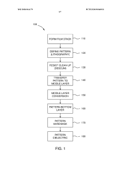
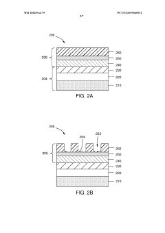
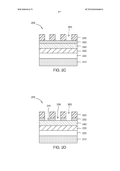
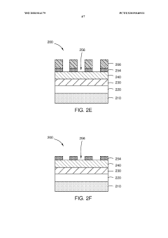
Patterning scheme to improve EUV resist and hard mask selectivity
PatentWO2020014179A1
Innovation
- A method involving a film stack with a bottom layer of diamond-like carbon, a middle layer that can be selectively etched relative to a photoresist, and a hard mask structure, where the middle layer is converted to increase etch selectivity, using EUV radiation and plasma processes to achieve high selectivity and minimize linewidth variations.
Reducing roughness of extreme ultraviolet lithography resists
PatentWO2020190941A1
Innovation
- Depositing a conformal thin film with less compressive or tensile stress than the resist using plasma-enhanced atomic layer deposition (ALD) to reduce the composite stress, thereby decreasing low-frequency roughness, and optionally etching the substrate to maintain pattern integrity.


Semiconductor Manufacturing Standards and Regulations
The semiconductor manufacturing industry operates under a comprehensive framework of standards and regulations that directly impact lithography processes, particularly concerning line edge roughness (LER) control in both EUV and optical lithography systems. International standards organizations such as SEMI, ISO, and ITRS have established critical specifications that define acceptable LER tolerances for different technology nodes, with increasingly stringent requirements as feature sizes continue to shrink.
SEMI standards, particularly SEMI P37 and related metrology guidelines, establish standardized measurement protocols for LER characterization across different lithography platforms. These standards mandate specific statistical analysis methods, sampling frequencies, and measurement conditions that ensure consistent evaluation of both EUV and optical lithography performance. The standards also define correlation methodologies between different metrology tools, enabling accurate comparison of LER performance across various manufacturing environments.
Regulatory compliance requirements vary significantly across global markets, with regions like the United States, European Union, and Asia-Pacific implementing distinct oversight frameworks. The U.S. Department of Commerce export control regulations specifically address advanced lithography equipment, including EUV systems, while European REACH regulations impact the chemical materials used in photoresist formulations that directly influence LER characteristics.
Quality management standards such as ISO 9001 and automotive-specific IATF 16949 impose additional requirements for process control and documentation in semiconductor manufacturing. These standards mandate statistical process control implementations that directly affect LER monitoring and control strategies, requiring manufacturers to maintain detailed records of lithography performance metrics and implement corrective actions when LER specifications are exceeded.
Environmental regulations, including waste disposal requirements for photoresist chemicals and energy consumption standards, influence the selection between EUV and optical lithography technologies. EUV systems typically require more complex environmental controls due to their vacuum operation and higher power consumption, necessitating compliance with additional safety and environmental standards that can impact overall manufacturing cost structures and operational procedures.
Cost-Performance Trade-offs in Lithography Selection
The selection between EUV and optical lithography involves complex cost-performance considerations that extend beyond simple equipment acquisition costs. While EUV lithography systems require significantly higher capital investment, often exceeding $200 million per tool compared to $50-80 million for advanced ArF immersion systems, the total cost of ownership analysis reveals a more nuanced picture when factoring in throughput, yield, and operational efficiency.
EUV lithography demonstrates superior performance in achieving critical dimensions below 7nm, delivering enhanced line edge roughness control that directly translates to improved device performance and higher yields. This performance advantage becomes economically compelling when the reduced number of patterning steps eliminates multiple exposure and etching processes required in optical lithography's multi-patterning approaches. The simplified process flow can reduce manufacturing cycle time by 20-30% for advanced nodes.
However, EUV adoption faces significant operational cost challenges. The technology's lower throughput, typically 140-170 wafers per hour compared to 250-300 for optical systems, increases per-wafer processing costs. Additionally, EUV requires specialized infrastructure including tin debris mitigation systems, hydrogen-free environments, and frequent pellicle replacements, contributing to elevated operational expenses.
The economic crossover point varies by application and production volume. For high-volume production of advanced processors and memory devices where line edge roughness directly impacts performance and yield, EUV's superior pattern fidelity justifies the premium costs. Conversely, for mature nodes or cost-sensitive applications, optical lithography with established multi-patterning techniques remains economically advantageous despite increased process complexity.
Emerging hybrid approaches optimize cost-performance by strategically deploying EUV for critical layers requiring precise edge control while utilizing optical lithography for less demanding features. This selective implementation strategy allows manufacturers to capture EUV's performance benefits while managing overall production costs, representing an increasingly popular approach for balancing technological advancement with economic viability in semiconductor manufacturing.
Unlock deeper insights with PatSnap Eureka Quick Research — get a full tech report to explore trends and direct your research. Try now!
Generate Your Research Report Instantly with AI Agent
Supercharge your innovation with PatSnap Eureka AI Agent Platform!