

Comparing Laser-etched vs Molded Waveguide Gratings
APR 14, 20269 MIN READ
Generate Your Research Report Instantly with AI Agent
Patsnap Eureka helps you evaluate technical feasibility & market potential.
Waveguide Grating Technology Background and Objectives
Waveguide gratings represent a fundamental component in modern photonic systems, serving as critical elements for wavelength-selective operations in optical communications, sensing applications, and integrated photonic circuits. These structures function by creating periodic variations in the effective refractive index along the waveguide propagation direction, enabling precise control over light propagation characteristics including reflection, transmission, and dispersion properties.
The evolution of waveguide grating technology has been driven by the increasing demand for higher performance optical devices with enhanced functionality and reduced manufacturing costs. Traditional fabrication approaches have primarily relied on photolithographic techniques combined with etching processes, which have established the foundation for current grating implementations in silicon photonics and other material platforms.
Recent technological developments have introduced alternative manufacturing methodologies, particularly molding-based approaches that promise to revolutionize the production scalability and cost-effectiveness of waveguide gratings. This paradigm shift represents a significant departure from conventional subtractive manufacturing processes toward additive and replicative techniques that can potentially achieve comparable or superior optical performance characteristics.
The comparative analysis between laser-etched and molded waveguide gratings addresses a critical technological decision point that impacts both performance optimization and manufacturing economics. Laser-etched gratings offer precise control over grating parameters through direct writing capabilities, enabling rapid prototyping and customization for specific applications. Conversely, molded gratings present opportunities for high-volume production with consistent quality and reduced per-unit costs.
The primary objective of this technological investigation centers on establishing comprehensive performance benchmarks and manufacturing feasibility assessments for both fabrication approaches. Key evaluation criteria include optical efficiency, spectral characteristics, dimensional accuracy, production scalability, and long-term reliability under operational conditions.
Furthermore, this analysis aims to identify the optimal application domains for each technology, considering factors such as production volume requirements, performance specifications, cost constraints, and integration complexity. The ultimate goal involves providing strategic guidance for technology selection and development roadmap planning in waveguide grating implementations across diverse photonic applications.
Market Demand for Laser-etched and Molded Waveguide Solutions
The telecommunications and photonics industries are experiencing unprecedented growth driven by the exponential demand for high-speed data transmission, cloud computing infrastructure, and emerging technologies such as 5G networks and autonomous vehicles. This surge has created substantial market opportunities for advanced optical components, particularly waveguide gratings that serve as critical elements in optical communication systems, sensors, and integrated photonic devices.
Laser-etched waveguide gratings have gained significant traction in high-performance applications where precision and customization are paramount. The aerospace and defense sectors represent key markets, where stringent performance requirements justify premium pricing for laser-etched solutions. Research institutions and specialized optical component manufacturers increasingly favor laser-etched gratings for prototyping and low-volume production runs, particularly in applications requiring unique specifications or rapid design iterations.
The telecommunications infrastructure market demonstrates strong demand for both manufacturing approaches, with selection criteria heavily influenced by deployment scale and performance requirements. Data center operators and network equipment manufacturers often require large quantities of standardized components, creating favorable conditions for molded waveguide solutions. The cost-effectiveness of molded gratings becomes particularly attractive in high-volume deployments where consistent performance across thousands of units is essential.
Consumer electronics applications, including augmented reality devices, LiDAR systems, and optical sensors, represent an emerging market segment with distinct requirements. These applications typically demand cost-effective solutions that can be manufactured at scale while maintaining acceptable performance levels. Molded waveguide gratings align well with these market needs, offering the potential for mass production at competitive price points.
The industrial sensing and measurement market presents opportunities for both technologies, with application-specific requirements driving technology selection. High-precision measurement systems often justify the premium associated with laser-etched gratings, while process monitoring and quality control applications may prioritize the cost advantages of molded solutions.
Geographic market dynamics reveal varying preferences across regions, with established photonics clusters in North America and Europe showing higher adoption rates for laser-etched solutions, while Asian markets demonstrate strong demand for cost-effective molded alternatives driven by large-scale manufacturing requirements.
Current Status and Challenges in Waveguide Grating Fabrication
Waveguide grating fabrication has reached a critical juncture where traditional manufacturing approaches face increasing demands for precision, scalability, and cost-effectiveness. Current fabrication methods primarily encompass laser etching and molding techniques, each presenting distinct advantages and limitations that significantly impact their adoption across different applications and market segments.
Laser etching technology has established itself as a dominant force in high-precision waveguide grating production, particularly for research applications and specialized optical components. This approach offers exceptional flexibility in pattern design and rapid prototyping capabilities, enabling manufacturers to achieve sub-micron feature sizes with remarkable accuracy. However, the technology faces substantial challenges in throughput limitations and equipment costs, making it economically challenging for large-scale production scenarios.
Molding-based fabrication represents the alternative pathway, leveraging replication techniques to achieve high-volume manufacturing at reduced per-unit costs. This approach excels in mass production environments where consistent grating structures are required across thousands of components. Nevertheless, molding techniques encounter significant obstacles in achieving the ultra-fine feature resolution demanded by advanced optical applications, particularly in telecommunications and sensing systems where grating precision directly correlates with performance metrics.
The industry currently grapples with fundamental trade-offs between manufacturing precision and production scalability. Laser etching systems, while capable of producing gratings with periodicities below 100 nanometers, typically operate at processing speeds that limit commercial viability for high-volume applications. Conversely, molding processes can achieve impressive throughput rates but struggle to maintain dimensional accuracy across complex grating geometries, particularly when dealing with non-uniform pitch distributions or chirped grating structures.
Material compatibility presents another significant challenge affecting both fabrication approaches. Laser etching processes must contend with thermal effects and material ablation characteristics that vary significantly across different substrate materials, from silicon-on-insulator platforms to polymer-based waveguides. Molding techniques face constraints related to mold durability, release agent compatibility, and the mechanical properties of replication materials, which directly influence the fidelity of transferred grating patterns.
Quality control and metrology represent persistent challenges across both fabrication methodologies. The verification of grating parameters, including pitch accuracy, sidewall angles, and surface roughness, requires sophisticated measurement techniques that often approach the resolution limits of available instrumentation. This measurement complexity becomes particularly acute when comparing gratings produced through different fabrication routes, as each method introduces characteristic defect signatures and dimensional variations that must be carefully characterized and controlled.
Current Laser-etching vs Molding Technical Solutions
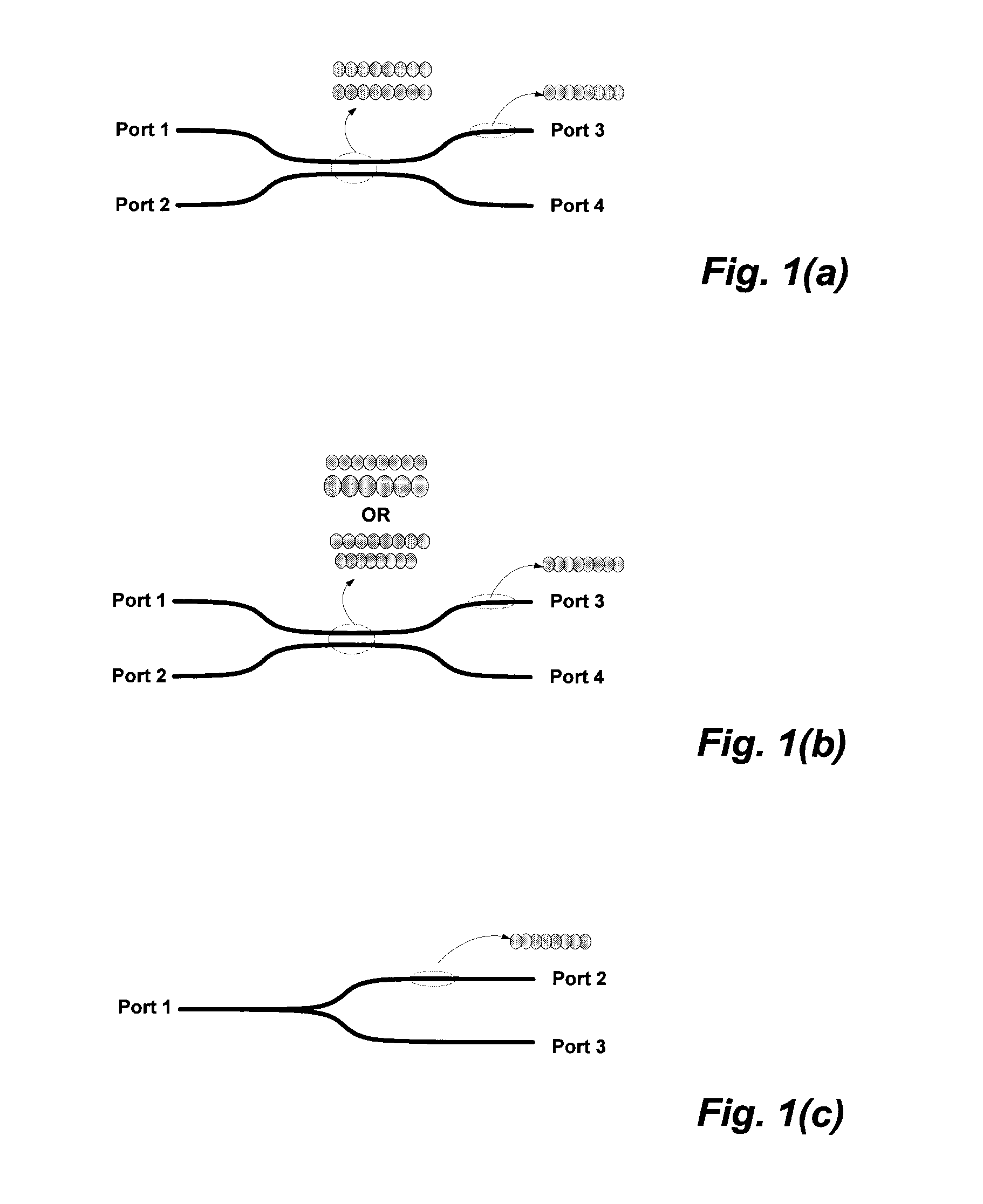
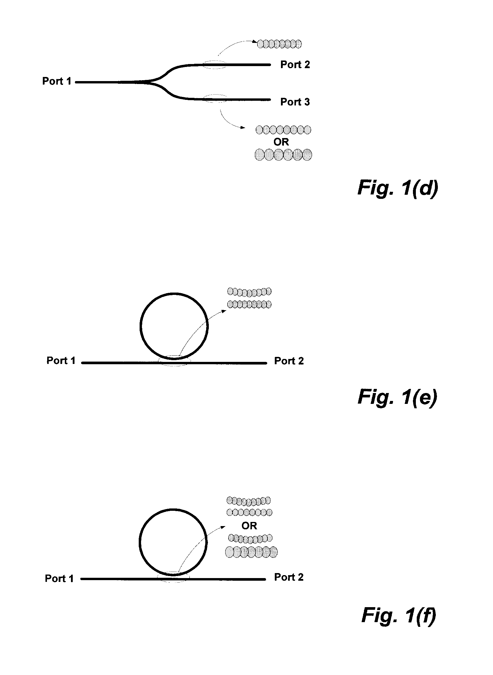
01 Waveguide grating structures for optical coupling and light manipulation
Waveguide gratings can be designed with specific structural configurations to efficiently couple light into and out of waveguides. These structures utilize periodic patterns or refractive index modulations to control light propagation, diffraction, and beam steering. The grating parameters such as period, depth, and duty cycle can be optimized to achieve desired optical performance for various wavelengths and applications.- Waveguide grating structures for optical coupling and light manipulation: Waveguide gratings can be designed with specific structural configurations to efficiently couple light into and out of waveguides. These structures utilize periodic patterns or refractive index modulations to control light propagation, diffraction, and beam steering. The grating parameters such as period, depth, and duty cycle can be optimized to achieve desired optical performance including coupling efficiency and wavelength selectivity.
- Diffractive optical elements using waveguide gratings for display applications: Waveguide gratings serve as key components in near-eye display systems and augmented reality devices. These diffractive elements enable in-coupling, propagation, and out-coupling of image-bearing light within thin waveguide substrates. The grating designs facilitate pupil expansion and field of view enhancement while maintaining compact form factors suitable for wearable display technologies.
- Fabrication methods for waveguide grating formation: Various manufacturing techniques can be employed to create waveguide gratings including lithographic patterning, etching processes, holographic recording, and nanoimprint methods. These fabrication approaches enable precise control over grating geometry and can be adapted for different substrate materials. Process optimization focuses on achieving high fidelity pattern transfer, minimizing defects, and enabling scalable production for commercial applications.
- Wavelength-selective waveguide gratings for optical filtering and sensing: Waveguide gratings can be engineered to exhibit wavelength-dependent reflection or transmission characteristics, enabling their use as optical filters and sensors. The spectral response can be tailored through grating design parameters to achieve narrow bandwidth filtering or multi-wavelength operation. Applications include wavelength division multiplexing, spectroscopic analysis, and environmental sensing where selective optical response is required.
- Polarization control using waveguide grating structures: Waveguide gratings can be designed to manipulate the polarization state of propagating light through anisotropic grating structures or form-birefringent patterns. These polarization-sensitive elements enable functions such as polarization beam splitting, polarization conversion, and polarization-dependent routing. The grating geometry and material properties can be optimized to achieve high polarization extinction ratios and broad operational bandwidth for photonic integrated circuits and optical communication systems.
02 Surface relief gratings and fabrication methods
Surface relief gratings feature physical surface modulations that create periodic structures on waveguide surfaces. Various fabrication techniques including lithography, etching, and molding processes can be employed to create these relief patterns. The manufacturing methods enable precise control over grating dimensions and profiles, which directly impact the optical characteristics and efficiency of the waveguide system.Expand Specific Solutions03 Diffractive optical elements for augmented reality and display applications
Waveguide gratings serve as key components in augmented reality displays and near-eye optical systems. These diffractive elements enable image projection, field of view expansion, and eyebox enlargement. The grating designs can incorporate multiple coupling regions including input couplers, intermediate gratings, and output couplers to achieve uniform light distribution and high-quality image reproduction for immersive visual experiences.Expand Specific Solutions04 Wavelength-selective and multiplexing waveguide gratings
Specialized waveguide gratings can be configured to selectively operate at specific wavelengths or handle multiple wavelength channels simultaneously. These wavelength-dependent characteristics enable applications in optical communications, spectroscopy, and color management. The grating designs may incorporate chirped structures, blazed profiles, or stacked configurations to achieve wavelength selectivity and efficient multiplexing capabilities.Expand Specific Solutions05 Polarization control and beam shaping with waveguide gratings
Waveguide gratings can be engineered to manipulate polarization states and control beam characteristics of propagating light. These gratings may feature anisotropic structures or specialized geometries that enable polarization-dependent diffraction, beam splitting, or polarization conversion. Such capabilities are valuable for applications requiring precise control over light polarization and spatial beam profiles in integrated photonic systems.Expand Specific Solutions
Key Players in Waveguide Grating Manufacturing Industry
The waveguide grating technology sector is experiencing rapid evolution, transitioning from early-stage research to commercial maturity. The market demonstrates significant growth potential driven by increasing demand for optical communication systems and photonic integrated circuits. Technology maturity varies considerably across different approaches, with laser-etched gratings showing advanced development through companies like Applied Materials, Intel Corp., and Coherent Inc., who leverage sophisticated semiconductor manufacturing capabilities. Molded waveguide gratings represent an emerging alternative, with players such as Nichia Corp., TDK Corp., and specialized photonics firms like Rockley Photonics Ltd. exploring cost-effective manufacturing solutions. Academic institutions including MIT, Zhejiang University, and University of Manchester contribute fundamental research, while telecommunications giants like NTT Inc. and Cisco Technology Inc. drive market adoption. The competitive landscape features established semiconductor manufacturers competing with specialized photonics companies, creating a dynamic environment where both precision laser-etching and scalable molding approaches vie for market dominance.
Applied Materials, Inc.
Technical Solution: Applied Materials develops advanced laser etching systems for waveguide grating fabrication, utilizing precision excimer laser technology with sub-micron accuracy. Their laser-etched approach enables rapid prototyping and customization of grating structures with flexible pitch control ranging from 100nm to 2μm. The company's process integration capabilities allow for seamless incorporation into existing semiconductor manufacturing lines, supporting both research and high-volume production requirements. Their laser systems achieve etch depths with ±5nm precision and can process various substrate materials including silicon, silicon nitride, and polymer waveguides.
Strengths: High precision control, flexible design modifications, excellent process integration. Weaknesses: Higher equipment costs, potential thermal damage to sensitive materials, slower throughput compared to molded alternatives.
Intel Corp.
Technical Solution: Intel employs both laser-etched and molded waveguide grating technologies in their silicon photonics platform. Their laser-etched gratings utilize advanced deep-UV lithography combined with reactive ion etching for precise grating definition in silicon-on-insulator substrates. The molded approach involves nanoimprint lithography using pre-fabricated masters, enabling high-throughput manufacturing of uniform grating structures. Intel's hybrid approach allows optimization based on application requirements, with laser-etched gratings for custom designs and molded gratings for volume production. Their manufacturing process achieves coupling efficiencies exceeding 90% with both approaches.
Strengths: Mature silicon photonics platform, scalable manufacturing, proven reliability in data center applications. Weaknesses: Limited to silicon-based materials, high initial development costs for new grating designs.
Core Patents in Advanced Waveguide Grating Fabrication
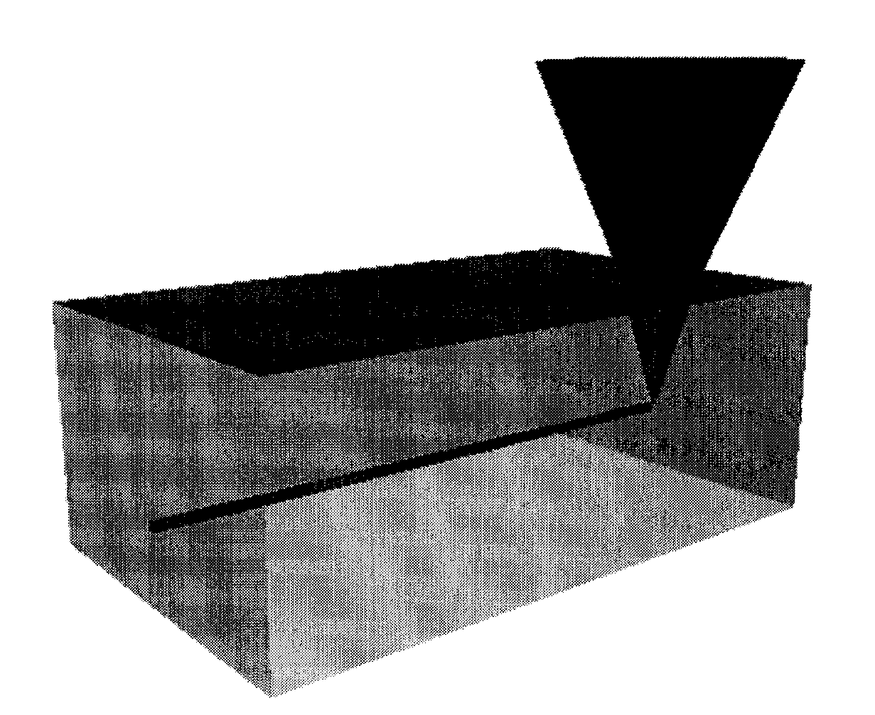
Method of manufacturing grating
PatentInactiveUS6690860B2
Innovation
- A method involving controlled scanning of a laser beam along the optical waveguide with a predetermined speed and multiple passes to achieve a uniform irradiation distribution, using a thermal conductive substrate to dissipate heat and a pulse laser with high energy density, while monitoring the reflected beam for precise alignment.


Optical devices and digital laser method for writing waveguides, gratings, and integrated optical circuits
PatentActiveUS20090304331A1
Innovation
- A method for simultaneous point-by-point fabrication of gratings and waveguides using a pulsed laser to create periodic structures in transparent substrates, allowing for flexible 3D path integration and varying grating periods for complex optical circuits, with the ability to form both low-loss waveguides and periodic or chirped gratings in a single step.

Manufacturing Cost Analysis for Waveguide Grating Methods
The manufacturing cost structure for waveguide grating production varies significantly between laser-etched and molded approaches, with each method presenting distinct economic advantages and limitations across different production scenarios.
Laser-etched waveguide gratings require substantial initial capital investment in precision laser systems, typically ranging from $500,000 to $2 million for industrial-grade equipment capable of achieving sub-micron accuracy. The operational costs include high energy consumption, specialized maintenance requirements, and skilled technician wages. However, this method offers exceptional flexibility for prototyping and small-batch production, with minimal setup costs for design changes and rapid turnaround times.
The per-unit manufacturing cost for laser etching remains relatively constant regardless of production volume, making it economically viable for low to medium volume applications. Material waste is minimal since the process is subtractive and highly precise, though the processing time per unit can be substantial for complex grating patterns.
Molded waveguide grating production presents a contrasting cost profile, characterized by high initial tooling investments ranging from $100,000 to $500,000 per mold design. The mold fabrication process requires specialized precision machining or electron beam lithography, contributing to extended lead times and significant upfront costs. However, once tooling is established, the per-unit production costs decrease dramatically with volume.
The molding approach demonstrates superior cost efficiency for high-volume manufacturing, with per-unit costs potentially dropping to 10-20% of laser-etched equivalents at production volumes exceeding 10,000 units. Material utilization efficiency is high, and cycle times are significantly shorter, enabling rapid throughput once production begins.
Labor costs differ substantially between methods, with laser etching requiring highly skilled operators for equipment setup and quality control, while molding operations can utilize less specialized personnel for routine production tasks. Quality control expenses also vary, as laser-etched products require individual inspection, whereas molded gratings benefit from consistent tooling-based replication.
The break-even analysis typically favors laser etching for volumes below 1,000-5,000 units, depending on grating complexity, while molding becomes increasingly cost-effective for larger production runs. Additionally, the total cost of ownership must consider equipment depreciation, maintenance schedules, and technology obsolescence risks, which tend to favor the more established molding infrastructure for long-term production commitments.
Quality Control Standards for Waveguide Grating Products
Quality control standards for waveguide grating products require distinct approaches when comparing laser-etched versus molded manufacturing processes. The fundamental difference in production methods necessitates tailored quality assurance protocols that address the unique characteristics and potential failure modes of each technology.
For laser-etched waveguide gratings, quality control standards must emphasize dimensional precision and surface integrity parameters. Critical measurements include grating period accuracy within ±5 nanometers, duty cycle uniformity across the entire grating length, and sidewall angle consistency. Surface roughness specifications typically require Ra values below 2 nanometers to minimize scattering losses. Thermal stability testing becomes crucial due to the laser processing effects on material properties.
Molded waveguide gratings demand different quality control criteria focused on replication fidelity and material homogeneity. Standards must verify complete pattern transfer from master templates, with particular attention to corner rounding and feature degradation. Residual layer thickness uniformity and demolding-induced stress patterns require systematic monitoring through optical and mechanical testing protocols.
Optical performance standards apply universally but with technology-specific tolerances. Insertion loss specifications for laser-etched gratings typically allow higher values due to processing-induced imperfections, while molded gratings must meet tighter coupling efficiency requirements. Wavelength accuracy standards generally favor laser-etched products, which can achieve sub-nanometer precision, compared to molded gratings limited by thermal expansion coefficients.
Environmental testing protocols must account for manufacturing-specific vulnerabilities. Laser-etched gratings require enhanced thermal cycling tests to evaluate heat-affected zone stability, while molded products need comprehensive humidity and chemical resistance testing due to polymer material properties. Accelerated aging standards should reflect the different degradation mechanisms inherent to each production method.
Statistical process control implementation varies significantly between technologies. Laser-etched production benefits from real-time monitoring of laser parameters and beam quality, while molded manufacturing requires continuous tracking of temperature profiles, pressure distributions, and cycle times. Sampling strategies must accommodate the different production volumes and cost structures typical of each approach.
Unlock deeper insights with Patsnap Eureka Quick Research — get a full tech report to explore trends and direct your research. Try now!
Generate Your Research Report Instantly with AI Agent
Supercharge your innovation with Patsnap Eureka AI Agent Platform!