

Comparing Optical Backplanes vs PCBs for Data Transmission Speed
MAY 20, 20269 MIN READ
Generate Your Research Report Instantly with AI Agent
PatSnap Eureka helps you evaluate technical feasibility & market potential.
Optical Backplane Technology Background and Objectives
Optical backplane technology emerged from the fundamental limitations of traditional electrical interconnects in high-performance computing and telecommunications systems. As data processing demands escalated exponentially over the past two decades, conventional printed circuit board (PCB) architectures began encountering significant bottlenecks in signal integrity, power consumption, and thermal management. The transition from electrical to optical interconnects represents a paradigm shift driven by the physics of electromagnetic wave propagation and the inherent advantages of photonic signal transmission.
The historical development of optical backplanes traces back to early fiber optic communication breakthroughs in the 1970s, evolving through successive generations of wavelength division multiplexing, integrated photonics, and silicon photonics technologies. Initial implementations focused primarily on long-haul telecommunications, but technological maturation has enabled miniaturization and cost reduction suitable for short-reach interconnect applications within computing systems.
Current market drivers include the exponential growth of data center traffic, artificial intelligence workloads, and high-frequency trading applications that demand ultra-low latency communication. The proliferation of cloud computing architectures and edge computing deployments has intensified requirements for high-bandwidth, low-power interconnect solutions that can maintain signal quality across increasingly dense system configurations.
The primary technical objective of optical backplane technology centers on achieving multi-terabit aggregate bandwidth while maintaining signal integrity across short-reach connections typically spanning centimeters to meters within system enclosures. Unlike traditional PCB traces that suffer from frequency-dependent losses, crosstalk, and electromagnetic interference, optical channels can theoretically support unlimited bandwidth with minimal signal degradation.
Power efficiency represents another critical objective, as optical transmission can potentially reduce energy consumption per bit transmitted compared to high-speed electrical signaling. This becomes particularly significant in large-scale deployments where cumulative power savings translate to substantial operational cost reductions and improved thermal management.
Latency minimization constitutes a fundamental goal, especially for applications requiring deterministic timing characteristics. Optical signals propagate at approximately two-thirds the speed of light in typical waveguide materials, potentially offering latency advantages over electrical transmission through PCB traces with complex routing constraints and signal conditioning requirements.
The technology aims to address scalability limitations inherent in electrical backplanes, where increasing channel density leads to diminishing returns due to crosstalk and power delivery challenges. Optical backplanes seek to enable higher port densities while maintaining consistent performance characteristics across all channels simultaneously.
Market Demand for High-Speed Data Transmission Solutions
The global demand for high-speed data transmission solutions has reached unprecedented levels, driven by the exponential growth of data-intensive applications across multiple industries. Cloud computing infrastructure, artificial intelligence workloads, and real-time analytics require increasingly sophisticated interconnect technologies capable of handling massive data volumes with minimal latency. Traditional copper-based transmission methods are approaching their physical limitations, creating substantial market pressure for advanced solutions.
Data centers represent the largest segment driving demand for high-speed transmission technologies. The proliferation of hyperscale facilities and edge computing deployments necessitates backplane architectures that can support multi-terabit throughput while maintaining signal integrity across complex routing paths. Enterprise customers are actively seeking solutions that can accommodate bandwidth scaling without requiring complete infrastructure overhauls, emphasizing the importance of forward-compatible transmission technologies.
Telecommunications infrastructure modernization presents another significant demand driver, particularly with the ongoing deployment of fifth-generation wireless networks and fiber-to-the-premises initiatives. Network equipment manufacturers require backplane solutions capable of supporting increased port densities and higher per-channel data rates while meeting stringent power efficiency requirements. The transition toward software-defined networking architectures further amplifies the need for flexible, high-performance interconnect solutions.
High-performance computing applications, including scientific research facilities and financial trading systems, generate substantial demand for ultra-low latency transmission solutions. These environments prioritize deterministic performance characteristics and minimal signal degradation over long interconnect distances. The growing adoption of machine learning accelerators and specialized processing units creates additional requirements for high-bandwidth, low-latency chip-to-chip communication pathways.
Manufacturing and industrial automation sectors increasingly rely on real-time data processing capabilities, driving demand for reliable high-speed transmission solutions in harsh operating environments. The integration of Internet of Things devices and industrial control systems requires robust interconnect technologies that can maintain performance under challenging thermal and electromagnetic conditions while supporting diverse protocol requirements across heterogeneous system architectures.
Current State and Challenges of Optical vs PCB Technologies
The current landscape of data transmission technologies presents a clear dichotomy between traditional PCB-based solutions and emerging optical backplane systems. PCB technology has reached significant maturity, with high-speed copper traces capable of supporting data rates up to 112 Gbps per lane using advanced signaling techniques like PAM4. However, these systems face fundamental physical limitations including signal attenuation, crosstalk, and electromagnetic interference that become increasingly problematic at higher frequencies and longer trace lengths.
Optical backplane technology represents a paradigm shift, utilizing light-based signal transmission through integrated photonic circuits and optical waveguides. Current optical solutions demonstrate superior performance characteristics, achieving data rates exceeding 400 Gbps per channel with minimal signal degradation over extended distances. Leading implementations incorporate silicon photonics platforms that enable dense integration of optical components directly onto substrates.
The primary challenge confronting optical backplanes lies in manufacturing complexity and cost considerations. Current production processes require specialized fabrication facilities and precise alignment tolerances measured in nanometers. Integration of optical components with electronic systems presents significant packaging challenges, particularly regarding thermal management and mechanical stability. Additionally, the ecosystem of supporting components, including optical connectors, transceivers, and control electronics, remains less mature compared to established PCB infrastructure.
PCB technology faces distinct limitations in next-generation applications. Signal integrity degradation becomes pronounced beyond 56 Gbps data rates, requiring increasingly sophisticated equalization and error correction mechanisms. Power consumption scales unfavorably with data rate increases, as higher-frequency signals demand greater drive strength to overcome channel losses. Geometric constraints limit achievable trace densities, creating bottlenecks in high-bandwidth applications.
Geographical distribution of technological capabilities reveals concentrated expertise in optical backplane development within established semiconductor hubs, particularly in North America and East Asia. PCB manufacturing capabilities remain more globally distributed, with established supply chains and manufacturing infrastructure. This disparity creates strategic considerations for technology adoption and supply chain resilience.
Current market dynamics indicate a transitional period where both technologies coexist, with optical solutions targeting high-performance applications while PCBs maintain dominance in cost-sensitive segments. The convergence point where optical backplanes achieve cost parity with high-speed PCB solutions represents a critical inflection point for widespread adoption across diverse application domains.
Existing Solutions for High-Speed Data Transmission
01 Optical signal transmission and processing in backplane systems
Advanced optical backplane systems utilize sophisticated signal transmission and processing techniques to achieve high-speed data communication. These systems employ optical switching, wavelength division multiplexing, and advanced modulation schemes to enhance data throughput. The optical components are integrated with electronic control systems to manage signal routing and maintain signal integrity across multiple channels.- Optical signal transmission and processing in backplane systems: Advanced optical backplane systems utilize sophisticated signal transmission and processing techniques to achieve high-speed data communication. These systems employ optical waveguides, fiber optic connections, and specialized optical components to transmit data at significantly higher speeds than traditional electrical connections. The optical approach reduces electromagnetic interference and enables parallel data transmission across multiple channels simultaneously.
- High-speed electrical interconnection methods for PCB systems: Traditional printed circuit board systems employ various electrical interconnection techniques to maximize data transmission speeds. These methods include optimized trace routing, differential signaling, impedance matching, and advanced connector designs. While electrical systems face limitations due to signal integrity issues at higher frequencies, they remain cost-effective and widely implemented in many applications.
- Hybrid optical-electrical integration architectures: Modern communication systems increasingly utilize hybrid architectures that combine both optical and electrical transmission methods to optimize performance and cost. These integrated approaches leverage the speed advantages of optical transmission for long-distance or high-bandwidth connections while maintaining electrical connections for shorter distances and control signals. This combination provides flexibility in system design and implementation.
- Signal integrity and noise reduction techniques: Both optical and electrical backplane systems require sophisticated signal integrity management to maintain high-speed data transmission. These techniques include advanced shielding methods, crosstalk reduction, jitter minimization, and error correction algorithms. Proper signal conditioning and filtering are essential for maintaining data integrity at high transmission speeds regardless of the underlying transmission medium.
- Bandwidth optimization and multiplexing strategies: Advanced multiplexing and bandwidth optimization techniques are employed in both optical and electrical systems to maximize data throughput. These strategies include wavelength division multiplexing for optical systems, time division multiplexing, and advanced modulation schemes. The implementation of these techniques allows for efficient utilization of available bandwidth and enables higher aggregate data transmission rates.
02 High-speed electrical interconnect technologies for PCB systems
Traditional printed circuit board systems achieve enhanced data transmission speeds through advanced electrical interconnect designs, including differential signaling, controlled impedance routing, and multi-layer stackup configurations. These technologies focus on minimizing signal loss, reducing crosstalk, and maintaining signal integrity at high frequencies through careful trace geometry and material selection.Expand Specific Solutions03 Hybrid optical-electrical interface systems
Innovative interface systems combine optical and electrical transmission methods to optimize data transfer performance. These hybrid approaches utilize optical components for long-distance, high-bandwidth transmission while maintaining electrical connections for local processing and control functions. The integration enables seamless conversion between optical and electrical signals with minimal latency.Expand Specific Solutions04 Signal integrity and noise reduction techniques
Advanced signal conditioning and noise reduction methods are employed to maintain data transmission quality in both optical and electrical systems. These techniques include error correction algorithms, signal amplification, filtering mechanisms, and electromagnetic interference shielding. The implementations focus on preserving signal fidelity while maximizing transmission speeds across various communication channels.Expand Specific Solutions05 Network architecture and routing optimization
Sophisticated network architectures and routing protocols are designed to maximize data throughput in both optical backplane and PCB-based systems. These solutions implement advanced switching matrices, load balancing algorithms, and adaptive routing mechanisms to efficiently manage data flow. The architectures support scalable configurations that can accommodate varying bandwidth requirements and system complexities.Expand Specific Solutions
Key Players in Optical Backplane and PCB Industry
The optical backplanes versus PCBs technology landscape represents a rapidly evolving sector driven by increasing demands for higher data transmission speeds in telecommunications and data centers. The industry is transitioning from mature PCB-based solutions to emerging optical technologies, with market growth fueled by 5G deployment and cloud computing expansion. Technology maturity varies significantly across players: established telecommunications giants like Huawei, ZTE, and Ericsson are advancing optical solutions, while traditional connector manufacturers such as Molex, Amphenol, and Samtec continue optimizing PCB technologies. Semiconductor leaders including Intel and Samsung are developing hybrid approaches, integrating optical components with electronic systems. The competitive landscape shows optical backplanes gaining momentum but PCBs maintaining dominance in cost-sensitive applications, creating a bifurcated market where both technologies coexist based on specific performance and economic requirements.
International Business Machines Corp.
Technical Solution: IBM has pioneered optical interconnect technologies for high-performance computing applications, developing integrated optical-electrical PCB solutions that embed optical waveguides directly within multilayer PCB substrates. Their approach uses polymer optical waveguides fabricated using standard PCB manufacturing processes, enabling 10-40Gbps data transmission with lower cost than discrete optical components. IBM's technology maintains compatibility with existing PCB assembly processes while providing optical connectivity for chip-to-chip and board-to-board communications, particularly targeting server and supercomputer applications where bandwidth density and power efficiency are critical performance factors.
Strengths: PCB manufacturing compatibility, cost-effective integration, high-performance computing focus. Weaknesses: Limited commercial availability, specialized application scope.
Molex LLC
Technical Solution: Molex provides optical connector and cable solutions that enable hybrid backplane architectures combining optical and electrical connectivity. Their optical backplane connectors support multi-mode and single-mode fiber connections with data rates up to 100Gbps, designed for telecommunications and data center applications. The company's solutions include active optical cables (AOCs) and embedded optical modules that can be integrated into traditional PCB-based systems, providing a migration path from purely electrical PCB designs to optical-enhanced architectures. Molex focuses on connector reliability and signal integrity for both optical and electrical domains within the same backplane system.
Strengths: Proven connector reliability, hybrid architecture support, industry-standard compatibility. Weaknesses: Component-level solution rather than system integration, dependent on customer system design.
Core Innovations in Optical Backplane Technologies
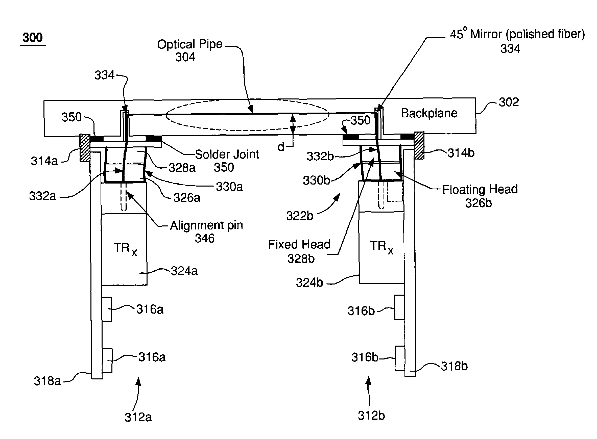
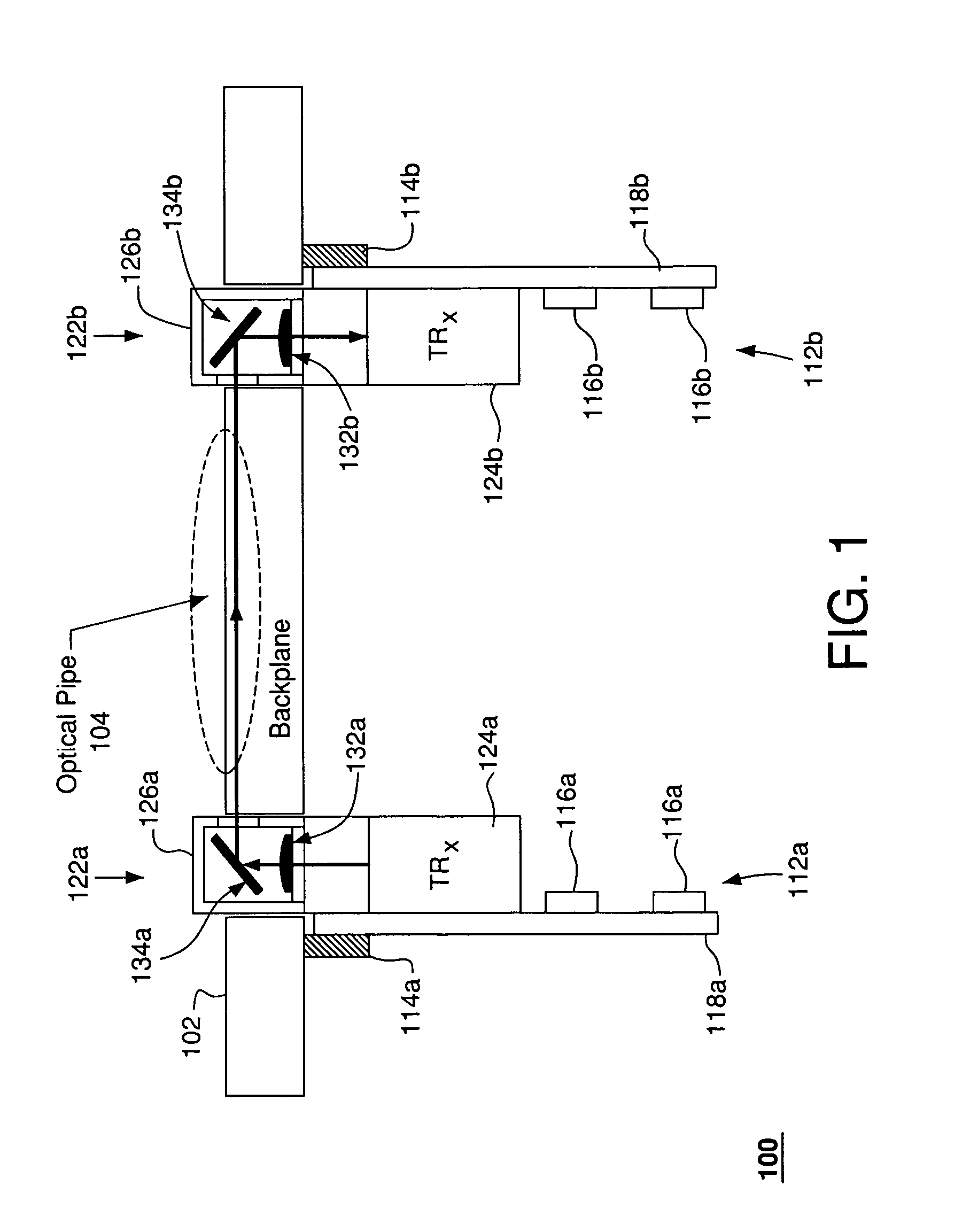
Coupler assembly for an optical backplane system
PatentInactiveUS7062132B2
Innovation
- A coupler assembly with movable optical elements, such as MEMS mirrors or flexible optical fibers, that can automatically adjust to maintain optical coupling by tracking changes in the relative position of the circuit pack and backplane, accommodating initial misalignment and subsequent deformations without operator intervention.
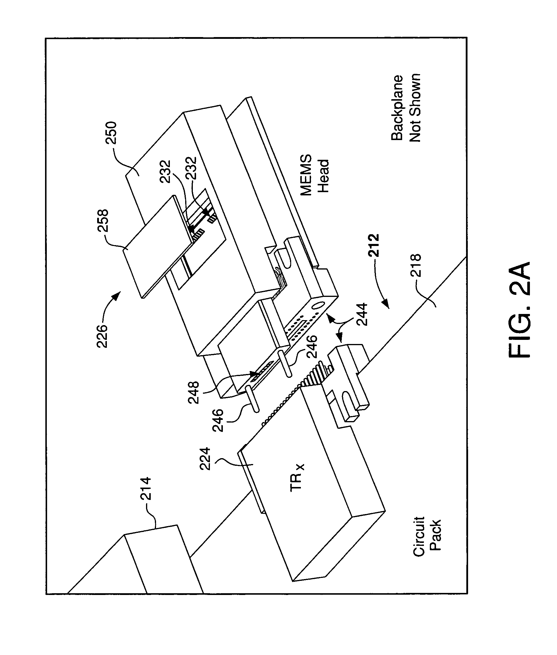

Optical backplane having at least one optical relay element for relaying light from an input facet of the backplane to an output facet of the backplane
PatentInactiveUS20120175535A1
Innovation
- An optical backplane design featuring a slab with parallel side walls and optical relay elements that reflect and refocus light beams to prevent divergence, allowing for more relaxed alignment tolerances and longer lengths without compromising signal integrity.


Manufacturing Standards for Optical Backplane Systems
The manufacturing of optical backplane systems requires adherence to stringent industry standards that ensure reliability, performance, and interoperability across different platforms. Current manufacturing standards are primarily governed by IEEE 802.3 specifications for Ethernet applications, IEC 61754 series for optical connector standards, and Telcordia GR-1221 for optical component reliability requirements. These standards establish critical parameters including insertion loss limits, return loss specifications, and environmental operating conditions that manufacturers must meet during production processes.
Quality control protocols in optical backplane manufacturing encompass multiple verification stages, from raw material inspection to final system integration testing. Manufacturing facilities typically implement ISO 9001 quality management systems alongside specialized optical testing procedures. Key manufacturing checkpoints include fiber alignment accuracy within ±0.5 micrometers, connector endface geometry verification according to IEC standards, and comprehensive optical power budget validation across all channels.
Precision assembly techniques represent a cornerstone of optical backplane manufacturing standards. Automated fiber placement systems ensure consistent positioning accuracy, while controlled environment conditions maintain temperature stability within ±2°C and humidity levels below 45% during critical assembly phases. Surface cleanliness standards require Class 10,000 cleanroom environments for connector assembly operations, with particle contamination limits strictly enforced to prevent optical signal degradation.
Testing and validation procedures follow established protocols including insertion loss measurements not exceeding 0.75dB per connection, return loss performance better than -20dB, and crosstalk isolation maintaining -30dB minimum separation between adjacent channels. Thermal cycling tests verify performance stability across -40°C to +85°C operating ranges, while mechanical durability testing ensures connector mating cycles exceed 500 operations without performance degradation.
Traceability requirements mandate comprehensive documentation throughout the manufacturing process, including component genealogy tracking, optical performance data recording, and calibration certificate maintenance for all test equipment. These standards collectively ensure that optical backplane systems deliver consistent high-speed data transmission performance while maintaining long-term reliability in demanding operational environments.
Cost-Performance Analysis of Optical vs PCB Solutions
The cost-performance analysis of optical versus PCB solutions reveals significant disparities in both initial investment requirements and long-term operational benefits. Optical backplane systems typically demand substantially higher upfront capital expenditure, with costs ranging from 3-5 times that of equivalent PCB implementations. This premium stems from sophisticated photonic components, precision manufacturing requirements, and specialized assembly processes that drive material and production costs significantly higher than traditional electronic solutions.
However, the performance advantages of optical systems justify the investment premium in high-throughput applications. Optical backplanes deliver bandwidth densities exceeding 10 Tbps per slot while maintaining signal integrity across longer distances without regeneration. This translates to reduced system complexity and lower power consumption per bit transmitted, particularly beneficial in data center environments where energy costs represent substantial operational expenses.
The total cost of ownership analysis demonstrates that optical solutions achieve cost parity with PCB systems at bandwidth requirements above 400 Gbps per channel. Beyond this threshold, the superior scalability and reduced infrastructure requirements of optical systems generate measurable cost advantages. The elimination of signal conditioning circuits, reduced cooling requirements, and extended operational lifespans contribute to favorable long-term economics despite higher initial investments.
Performance metrics reveal that optical backplanes maintain consistent signal quality regardless of transmission distance within typical chassis dimensions, while PCB solutions experience degradation requiring expensive signal processing circuits. The inherent electromagnetic immunity of optical systems reduces system-level design complexity and associated costs, particularly in high-density configurations where crosstalk mitigation becomes increasingly expensive in PCB implementations.
Market adoption patterns indicate that cost-performance crossover points continue shifting toward lower bandwidth thresholds as optical component manufacturing scales improve and PCB complexity costs increase. Current projections suggest optical solutions will achieve cost competitiveness at 200 Gbps channel rates within three years, accelerating adoption across broader application segments beyond current high-end implementations.
Unlock deeper insights with PatSnap Eureka Quick Research — get a full tech report to explore trends and direct your research. Try now!
Generate Your Research Report Instantly with AI Agent
Supercharge your innovation with PatSnap Eureka AI Agent Platform!