Comparing Wet vs Dry Etching in Semiconductor Fabrication
MAR 31, 20269 MIN READ
Generate Your Research Report Instantly with AI Agent
Patsnap Eureka helps you evaluate technical feasibility & market potential.
Semiconductor Etching Technology Background and Objectives
Semiconductor etching technology represents one of the most critical processes in modern microelectronics manufacturing, serving as the foundation for creating intricate patterns and structures on silicon wafers. The evolution of etching techniques has been driven by the relentless pursuit of smaller feature sizes, higher precision, and improved manufacturing efficiency in semiconductor fabrication.
The historical development of semiconductor etching began in the 1960s with simple wet chemical etching processes, which utilized liquid chemical solutions to remove material from semiconductor substrates. As the industry progressed through the 1970s and 1980s, the limitations of wet etching became apparent, particularly in achieving the precise dimensional control required for increasingly miniaturized devices. This led to the development and widespread adoption of dry etching techniques, including plasma etching, reactive ion etching (RIE), and deep reactive ion etching (DRIE).
The fundamental distinction between wet and dry etching lies in their material removal mechanisms and process environments. Wet etching employs liquid chemical solutions that react with the target material through isotropic chemical reactions, while dry etching utilizes gaseous plasmas and ion bombardment to achieve anisotropic material removal. This technological divergence has created two complementary yet distinct approaches to semiconductor patterning.
Current technological trends in semiconductor etching are primarily driven by the continuous scaling demands of Moore's Law and the emergence of three-dimensional device architectures. The industry faces unprecedented challenges in achieving sub-10 nanometer feature sizes while maintaining high aspect ratios and precise sidewall profiles. Advanced applications such as FinFET transistors, through-silicon vias (TSVs), and MEMS devices require sophisticated etching solutions that can deliver atomic-level precision.
The primary objectives of modern semiconductor etching technology encompass several critical performance metrics. Dimensional accuracy remains paramount, requiring etch processes that can maintain feature sizes within nanometer tolerances across entire wafer surfaces. Selectivity between different materials must be optimized to prevent unwanted material removal while ensuring complete pattern transfer. Surface quality and sidewall profile control are essential for maintaining device performance and reliability.
Process uniformity across large wafer areas represents another fundamental objective, as manufacturing economics demand consistent results across 300mm wafers and beyond. Contamination control and particle generation minimization are crucial for maintaining high yield rates in advanced semiconductor manufacturing. Additionally, environmental considerations and cost-effectiveness drive the development of more sustainable etching processes with reduced chemical consumption and waste generation.
The strategic importance of etching technology extends beyond traditional CMOS applications into emerging fields such as quantum computing, photonics, and advanced packaging technologies. These applications present unique challenges that require innovative etching solutions capable of processing novel materials and achieving unprecedented precision levels.
Market Demand Analysis for Advanced Etching Solutions
The global semiconductor industry continues to experience unprecedented growth, driven by expanding applications in artificial intelligence, 5G communications, Internet of Things devices, and automotive electronics. This surge in demand has created substantial market opportunities for advanced etching solutions, as manufacturers seek to achieve smaller feature sizes, higher aspect ratios, and improved device performance. The transition toward more complex three-dimensional structures and advanced materials has intensified the need for sophisticated etching technologies that can deliver precise control and superior selectivity.
Market dynamics reveal a clear bifurcation in etching solution demand based on application requirements and manufacturing scales. High-volume production facilities increasingly favor dry etching systems for their superior process control, automation capabilities, and ability to handle advanced node requirements below 10 nanometers. These facilities represent the largest revenue segment, as they require multiple etching chambers and frequent equipment upgrades to maintain competitive manufacturing capabilities.
Conversely, the wet etching segment maintains strong demand in specific market niches, particularly for legacy node production, specialized applications requiring isotropic etching profiles, and cost-sensitive manufacturing environments. Research institutions and smaller fabrication facilities continue to rely heavily on wet etching solutions due to lower capital investment requirements and operational simplicity. The market for wet etching chemicals and equipment remains stable, supported by ongoing production of mature semiconductor devices and specific process steps where wet chemistry offers advantages.
Regional market analysis indicates that Asia-Pacific dominates demand for both wet and dry etching solutions, accounting for the majority of global semiconductor manufacturing capacity. Leading foundries and memory manufacturers in this region drive significant investments in advanced dry etching equipment, while also maintaining substantial wet etching operations for specific process requirements. North American and European markets show strong demand for specialized etching solutions, particularly in research and development applications and niche manufacturing segments.
The competitive landscape reflects evolving customer preferences toward integrated solutions that combine multiple etching capabilities within single platforms. Equipment manufacturers are responding by developing hybrid systems that can perform both wet and dry etching processes, addressing market demand for flexibility and operational efficiency. This trend indicates growing market acceptance of versatile etching solutions that can adapt to diverse manufacturing requirements while optimizing facility utilization and reducing total cost of ownership.
Current Status and Challenges in Wet vs Dry Etching
The semiconductor industry currently employs both wet and dry etching technologies as fundamental processes in device fabrication, each serving distinct roles based on specific manufacturing requirements. Wet etching remains prevalent in applications requiring high selectivity and cost-effective processing, particularly for bulk material removal and cleaning operations. This chemical-based approach utilizes liquid etchants to dissolve target materials, offering excellent selectivity ratios and uniform etching across large wafer surfaces.
Dry etching technologies, including reactive ion etching (RIE) and deep reactive ion etching (DRIE), dominate advanced node manufacturing where precise dimensional control is critical. These plasma-based processes enable anisotropic etching profiles essential for high-aspect-ratio features in modern semiconductor devices. The technology has evolved to incorporate advanced plasma chemistries and sophisticated process control systems, making it indispensable for sub-10nm technology nodes.
Current wet etching faces significant limitations in achieving the dimensional precision required for advanced semiconductor geometries. The isotropic nature of chemical etching creates undercutting issues that compromise feature fidelity, particularly problematic for structures below 100nm. Additionally, wet processes struggle with high-aspect-ratio features due to transport limitations of etchant species and reaction byproducts within narrow trenches and vias.
Dry etching confronts challenges related to plasma-induced damage, including ion bombardment effects that can degrade device performance through crystal lattice disruption and charge accumulation. Etch selectivity remains a persistent issue, particularly when processing multi-layer stacks with similar materials. Process uniformity across large wafer areas presents ongoing difficulties, especially for 300mm and emerging 450mm wafer formats.
Geographically, wet etching technology development concentrates in established semiconductor manufacturing regions, with significant contributions from Japan, South Korea, and Taiwan focusing on chemical formulation optimization. Dry etching innovation centers primarily in the United States and Europe, where equipment manufacturers like Applied Materials and Lam Research drive plasma technology advancement. Asian foundries contribute substantially to process integration and manufacturing scalability improvements.
The integration of both technologies within modern fabrication flows creates additional complexity, requiring careful optimization of process sequences and contamination control between wet and dry processing steps. Cross-contamination prevention and wafer handling between different processing environments represent ongoing operational challenges that impact manufacturing efficiency and yield performance.
Current Wet and Dry Etching Process Solutions
01 Plasma etching methods and apparatus
Plasma etching techniques utilize ionized gases to remove material from semiconductor substrates. These methods involve controlling plasma parameters such as pressure, power, and gas composition to achieve precise etching profiles. The technology enables selective removal of materials while maintaining dimensional accuracy and minimizing damage to underlying layers. Advanced plasma etching systems incorporate feedback control mechanisms to optimize etch rates and uniformity across the substrate surface.- Plasma etching methods and apparatus: Plasma etching techniques utilize ionized gases to remove material from semiconductor substrates. These methods involve controlling plasma parameters such as pressure, power, and gas composition to achieve precise etching profiles. The technology enables selective removal of materials while maintaining dimensional accuracy and minimizing damage to underlying layers.
- Dry etching process control and optimization: Advanced dry etching processes focus on controlling etch rates, selectivity, and uniformity across wafer surfaces. These techniques employ real-time monitoring and feedback systems to adjust process parameters dynamically. The methods ensure consistent results in high-aspect-ratio features and complex pattern transfer applications.
- Wet chemical etching compositions and methods: Wet etching utilizes chemical solutions to selectively dissolve target materials from substrates. These formulations are designed to provide controlled etch rates with high selectivity between different material layers. The processes are particularly effective for isotropic etching applications and cleaning operations in semiconductor manufacturing.
- Etching equipment and chamber design: Specialized etching equipment incorporates advanced chamber designs to optimize process uniformity and throughput. These systems feature improved gas distribution, temperature control, and plasma confinement mechanisms. The designs enable better process repeatability and reduced particle contamination during etching operations.
- Selective etching and endpoint detection: Selective etching technologies enable precise material removal with high discrimination between different layers. Endpoint detection systems monitor process completion through optical emission spectroscopy or other sensing methods. These capabilities are critical for preventing over-etching and ensuring process reliability in multi-layer device fabrication.
02 Dry etching process control and optimization
Dry etching processes employ reactive gases and physical bombardment to remove material without liquid chemicals. Process control involves monitoring and adjusting parameters such as gas flow rates, chamber pressure, substrate temperature, and RF power to achieve desired etch characteristics. Optimization techniques focus on improving selectivity, anisotropy, and etch rate while reducing defects and maintaining process repeatability across multiple wafers.Expand Specific Solutions03 Wet chemical etching compositions and methods
Wet etching utilizes liquid chemical solutions to dissolve and remove specific materials from substrates. The compositions typically include acids, bases, or specialized etchants formulated to provide controlled etch rates and selectivity. Methods involve immersion, spray, or puddle techniques with precise timing and temperature control. The technology addresses challenges such as undercutting, surface roughness, and residue removal while ensuring compatibility with various substrate materials.Expand Specific Solutions04 Etching endpoint detection and monitoring systems
Endpoint detection technologies provide real-time monitoring of etching processes to determine when the desired etch depth or material removal is achieved. Systems employ optical emission spectroscopy, interferometry, or mass spectrometry to detect changes in plasma composition or reflected light patterns. These monitoring techniques enable precise process control, prevent over-etching, and improve yield by automatically stopping the etch process at the optimal point.Expand Specific Solutions05 Advanced etching for high aspect ratio structures
Specialized etching techniques address the challenges of creating deep, narrow features with high aspect ratios in semiconductor devices. These methods combine alternating etching and passivation steps to maintain vertical sidewalls and prevent lateral etching. Technologies include cryogenic etching, Bosch process variations, and atomic layer etching for nanoscale precision. The approaches enable fabrication of through-silicon vias, MEMS structures, and advanced memory devices with improved profile control and reduced surface damage.Expand Specific Solutions
Major Players in Semiconductor Etching Equipment Industry
The semiconductor etching landscape represents a mature, multi-billion-dollar market with distinct wet and dry etching segments serving complementary roles in advanced fabrication processes. The industry has reached technological maturity, with dry etching dominating critical patterning steps while wet etching remains essential for cleaning and material removal applications. Leading foundries including TSMC, Samsung Electronics, and SMIC demonstrate advanced capabilities across both etching methodologies, supported by specialized equipment manufacturers like Tokyo Electron, Applied Materials, and Advanced Micro Fabrication Equipment. The competitive environment features established Asian manufacturers such as SK Hynix, Nanya Technology, and Macronix International driving innovation in process optimization, while companies like ASML Netherlands and ULVAC provide critical supporting technologies. Market dynamics reflect ongoing consolidation around advanced node capabilities, with wet etching maintaining relevance for specific applications despite the industry's strategic focus on plasma-based dry etching solutions for next-generation semiconductor manufacturing requirements.
Samsung Electronics Co., Ltd.
Technical Solution: Samsung utilizes sophisticated wet and dry etching processes in their memory and logic fabrication facilities. Their wet etching approach employs buffered oxide etch (BOE) and phosphoric acid solutions for selective material removal with controlled etch rates of 10-100 nm/min depending on material and temperature. For dry etching, Samsung implements advanced plasma technologies including atomic layer etching (ALE) for precise material removal at the atomic scale, crucial for their 3D NAND structures with over 100 layers. Their process integration combines wet cleaning steps between dry etch processes to remove polymer residues and achieve smooth sidewall profiles. Samsung's proprietary etch recipes optimize the balance between etch rate, selectivity, and profile control for their advanced memory architectures including V-NAND and next-generation DRAM technologies.
Strengths: Strong vertical integration and advanced memory technology expertise. Weaknesses: Limited equipment supplier diversification and high process complexity management challenges.
Taiwan Semiconductor Manufacturing Co., Ltd.
Technical Solution: TSMC employs advanced wet and dry etching technologies across their leading-edge nodes. Their wet etching processes utilize selective chemical solutions for isotropic material removal, particularly effective for silicon dioxide and silicon nitride layers with high selectivity ratios exceeding 100:1. For dry etching, TSMC implements plasma-based reactive ion etching (RIE) and deep reactive ion etching (DRIE) systems that achieve anisotropic profiles with aspect ratios up to 50:1 for advanced FinFET and gate-all-around structures. Their hybrid approach combines both techniques strategically - wet etching for cleaning and isotropic requirements, dry etching for precise pattern transfer and high-aspect-ratio features essential for sub-5nm process nodes.
Strengths: Industry-leading process control and integration capabilities, extensive experience across multiple technology nodes. Weaknesses: High capital expenditure requirements and complex process optimization needs.
Key Technical Innovations in Etching Process Control
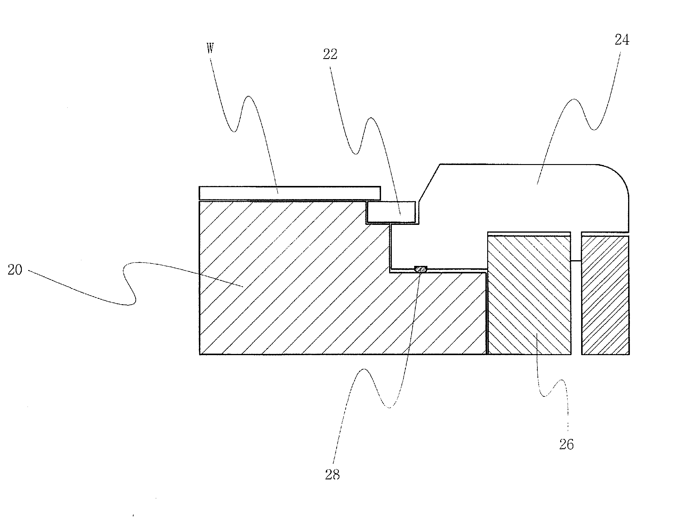
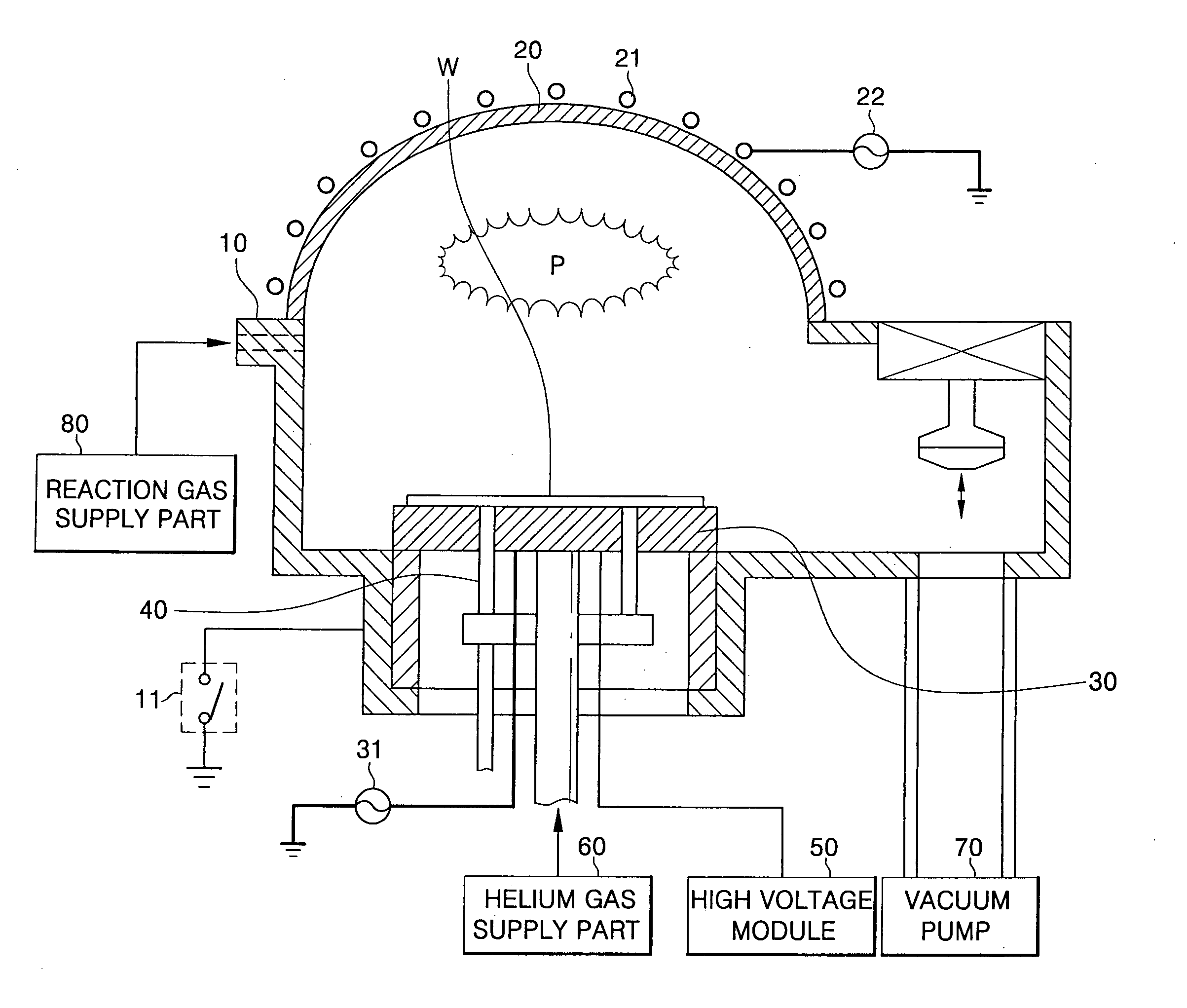
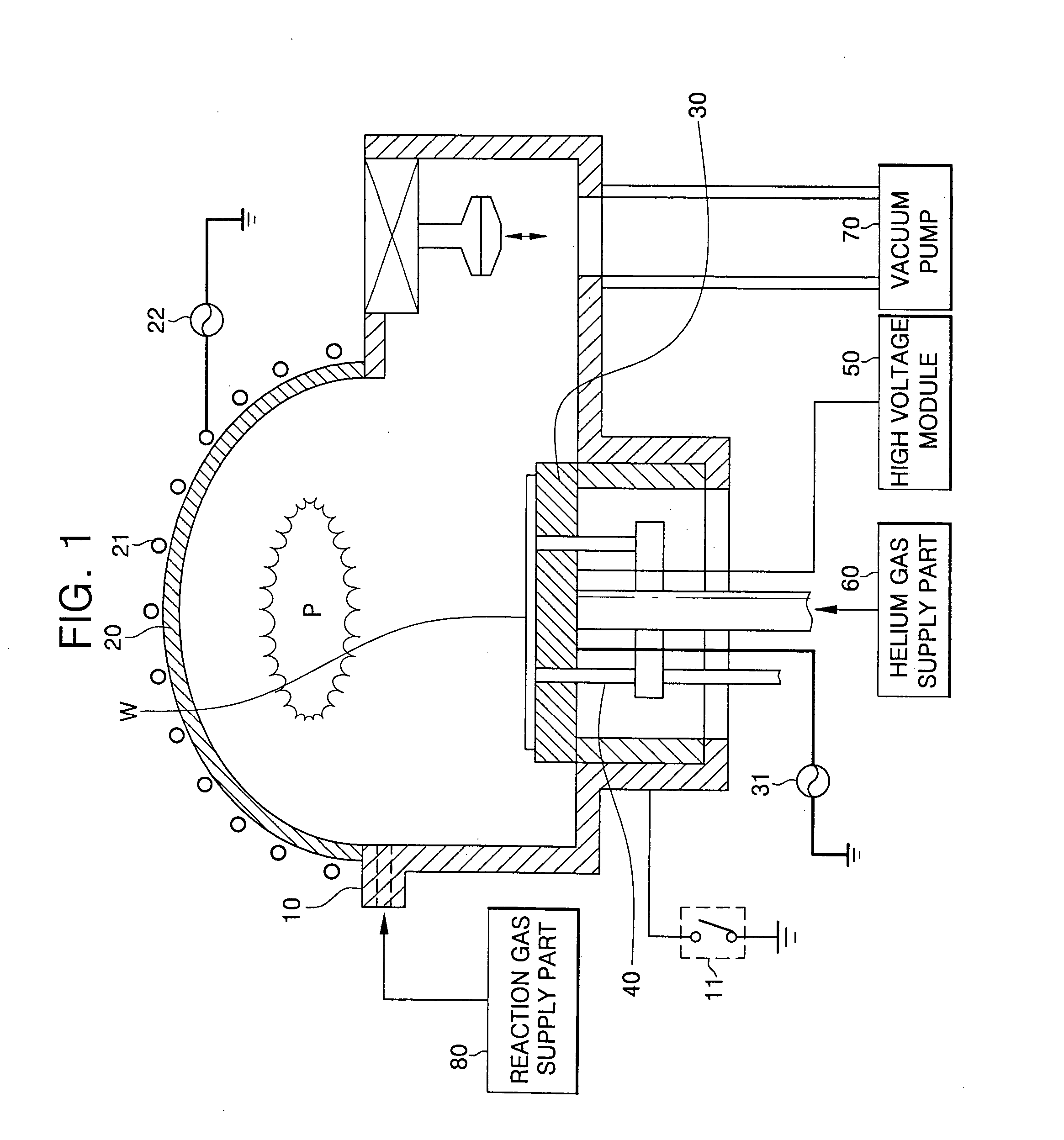
Methods and apparatus for semiconductor etching including an electro static chuck
PatentInactiveUS20080194113A1
Innovation
- A semiconductor etching apparatus with a gas flow blocking part, such as an O-ring, positioned in the vacuum path between the ESC and other parts to prevent polymer adsorption and helium leakage, ensuring stable plasma formation and etching uniformity.

Methods adapted for use in semiconductor processing apparatus including electrostatic chuck
PatentInactiveUS20060087793A1
Innovation
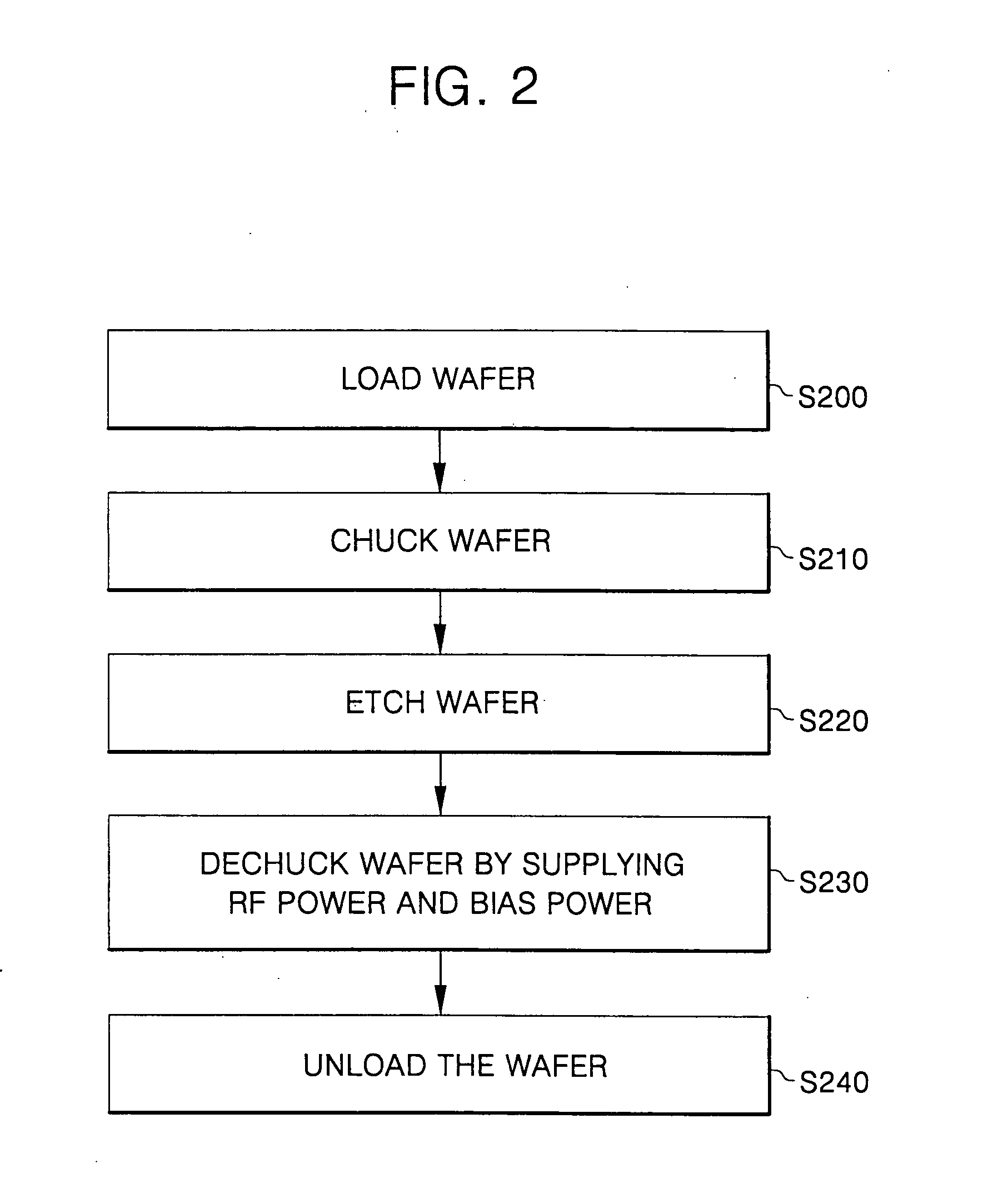
- A plasma processing method that applies both RF source power and bias power to generate de-chucking plasma, with specific power settings (400 W RF and 20-100 W bias power) to effectively discharge charges from the wafer, using argon or nitrogen gas, ensuring complete charge removal and secure wafer transfer.

Environmental Impact Assessment of Etching Processes
The environmental implications of wet and dry etching processes in semiconductor fabrication present distinct challenges and opportunities for sustainable manufacturing. Both methodologies generate different types of environmental impacts that require comprehensive assessment and mitigation strategies.
Wet etching processes primarily utilize liquid chemical solutions, including acids, bases, and organic solvents. These processes generate significant volumes of contaminated wastewater containing dissolved metals, acids, and organic compounds. The wastewater treatment requirements are substantial, necessitating neutralization systems, heavy metal precipitation, and advanced filtration technologies. Chemical consumption is considerable, with frequent solution replacement generating hazardous waste streams that require specialized disposal methods.
Dry etching processes, particularly plasma-based systems, present different environmental challenges. These processes consume substantial electrical energy and utilize fluorinated gases such as CF4, SF6, and NF3, which are potent greenhouse gases with high global warming potential. The atmospheric impact of these gases is significant, with some fluorinated compounds having atmospheric lifetimes exceeding 50,000 years.
Water consumption patterns differ markedly between the two approaches. Wet etching requires continuous fresh water supply for solution preparation and extensive rinsing operations, while dry etching primarily uses water for equipment cooling and chamber cleaning. However, dry etching's energy intensity often results in higher carbon footprint from electricity consumption.
Waste generation characteristics vary substantially. Wet etching produces liquid hazardous waste requiring treatment and disposal, while dry etching generates gaseous emissions that must be abated using specialized scrubbing systems. Modern semiconductor facilities employ point-of-use abatement systems for dry etching, achieving destruction efficiencies exceeding 95% for most process gases.
Resource efficiency considerations favor different aspects of each technology. Wet etching offers better material selectivity and uniformity but requires larger chemical inventories and generates more waste per unit processed. Dry etching provides superior process control and reduced chemical usage but demands higher energy input and specialized gas handling infrastructure.
Regulatory compliance requirements continue evolving, with increasing focus on greenhouse gas emissions reporting and reduction targets. The semiconductor industry faces mounting pressure to minimize perfluorinated compound emissions while maintaining manufacturing efficiency and product quality standards.
Cost-Benefit Analysis of Wet vs Dry Etching Methods
The cost-benefit analysis of wet versus dry etching methods reveals significant economic implications for semiconductor manufacturers. Initial capital expenditure represents a primary differentiator, with wet etching systems typically requiring 60-80% lower upfront investment compared to dry etching equipment. Basic wet etching stations cost approximately $50,000-200,000, while advanced plasma etching systems range from $500,000-3,000,000 depending on configuration and capabilities.
Operational expenses present a more complex comparison framework. Wet etching demonstrates superior cost efficiency in chemical consumption per wafer processed, particularly for bulk material removal applications. Chemical costs typically range from $0.05-0.15 per wafer for standard wet processes, while dry etching consumables including gases, chamber components, and maintenance materials average $0.20-0.50 per wafer. However, wet etching incurs substantial waste treatment and disposal costs, often adding 15-25% to operational expenses.
Throughput economics favor different methods depending on application requirements. Wet etching achieves higher batch processing efficiency for non-critical layers, processing 25-50 wafers simultaneously with cycle times of 10-30 minutes. Dry etching offers superior single-wafer processing control with typical cycle times of 2-15 minutes, enabling higher precision but potentially lower overall throughput for volume production.
Labor and maintenance costs significantly impact long-term economics. Wet etching requires extensive safety protocols and specialized waste handling, increasing labor costs by approximately 20-30%. Dry etching systems demand highly skilled technicians for maintenance and troubleshooting, with annual service contracts typically costing 8-12% of equipment value. Chamber cleaning and component replacement in plasma systems can result in 15-20% downtime compared to 5-8% for wet systems.
Quality-related cost implications must be considered in the overall economic assessment. Dry etching's superior dimensional control and reduced defect rates can improve yield by 2-5% for critical layers, potentially offsetting higher operational costs through increased revenue per wafer. Wet etching's isotropic nature may require additional processing steps or result in lower yields for advanced node applications, impacting overall profitability despite lower direct processing costs.
Unlock deeper insights with Patsnap Eureka Quick Research — get a full tech report to explore trends and direct your research. Try now!
Generate Your Research Report Instantly with AI Agent
Supercharge your innovation with Patsnap Eureka AI Agent Platform!