EUV Lithography in Non-Volatile Memory Production: Cost Efficiency
APR 2, 20268 MIN READ
Generate Your Research Report Instantly with AI Agent
Patsnap Eureka helps you evaluate technical feasibility & market potential.
EUV Lithography NVM Background and Objectives
Extreme Ultraviolet (EUV) lithography represents a revolutionary advancement in semiconductor manufacturing, utilizing 13.5 nanometer wavelength light to achieve unprecedented pattern resolution capabilities. This technology has emerged as the cornerstone for producing advanced semiconductor devices with feature sizes below 7 nanometers, fundamentally transforming the landscape of non-volatile memory (NVM) production.
The evolution of EUV lithography stems from the semiconductor industry's relentless pursuit of Moore's Law, where traditional deep ultraviolet (DUV) lithography reached physical limitations around the 10-nanometer node. The transition from 193-nanometer immersion lithography to EUV technology marked a paradigm shift, enabling single-exposure patterning for critical layers that previously required complex multiple patterning techniques.
In the context of non-volatile memory production, EUV lithography addresses the escalating demands for higher storage density, improved performance, and enhanced reliability in NAND flash memory, 3D NAND structures, and emerging memory technologies such as MRAM and ReRAM. The technology's ability to define intricate patterns with superior edge roughness control and dimensional accuracy directly impacts memory cell scaling and yield optimization.
The primary technical objectives driving EUV adoption in NVM manufacturing encompass achieving sub-20-nanometer critical dimensions with single exposure, reducing overlay errors to sub-2-nanometer precision, and maintaining throughput levels exceeding 150 wafers per hour. These targets are essential for enabling next-generation memory architectures including vertical NAND structures with layer counts exceeding 200 levels and advanced 3D memory configurations.
Cost efficiency considerations have become paramount as EUV systems represent capital investments exceeding $200 million per tool, accompanied by substantial operational expenses including specialized photoresists, pellicles, and maintenance requirements. The economic viability of EUV implementation in NVM production hinges on optimizing the balance between enhanced manufacturing capabilities and total cost of ownership, while simultaneously achieving competitive yield rates and cycle times that justify the significant infrastructure investment required for this cutting-edge lithography technology.
Market Demand for Advanced NVM Manufacturing
The global non-volatile memory market is experiencing unprecedented growth driven by the exponential expansion of data generation and storage requirements across multiple sectors. Cloud computing infrastructure, artificial intelligence applications, and edge computing deployments are creating substantial demand for high-performance memory solutions that can deliver superior speed, density, and reliability compared to traditional storage technologies.
Enterprise data centers represent the largest consumption segment for advanced NVM products, particularly 3D NAND flash memory and emerging storage-class memory technologies. The transition toward more sophisticated server architectures and the proliferation of solid-state drives in enterprise environments are driving requirements for memory devices manufactured with cutting-edge lithographic processes. These applications demand the precision and feature scaling capabilities that EUV lithography enables.
Consumer electronics markets are simultaneously pushing density and performance boundaries as smartphones, tablets, and laptops integrate increasingly sophisticated memory subsystems. The automotive sector is emerging as a significant growth driver, with autonomous vehicles and advanced driver assistance systems requiring robust, high-capacity memory solutions manufactured to stringent quality standards.
The semiconductor industry's transition to advanced process nodes below 10 nanometers has created a technological inflection point where traditional lithographic techniques reach fundamental limitations. Memory manufacturers are compelled to adopt EUV lithography to achieve the critical dimensions necessary for next-generation 3D NAND structures and emerging memory architectures such as 3D XPoint and resistive RAM technologies.
Market dynamics reveal a concentrated demand structure where leading memory manufacturers require substantial production volumes to justify EUV implementation costs. The capital-intensive nature of EUV-enabled fabrication facilities creates barriers to entry while simultaneously driving consolidation among memory producers. This concentration effect amplifies the importance of cost efficiency optimization in EUV-based manufacturing processes.
Regional demand patterns show strong growth in Asia-Pacific markets, particularly driven by Chinese memory manufacturers seeking technological independence and capacity expansion. North American and European markets focus primarily on specialized applications requiring advanced performance characteristics, creating distinct market segments with varying cost sensitivity profiles.
The emergence of new memory technologies and architectures continues to expand addressable market opportunities, with storage-class memory and persistent memory applications representing high-value segments where EUV lithography's precision capabilities justify premium manufacturing costs despite current economic challenges.
Current EUV Cost Challenges in NVM Production
EUV lithography implementation in non-volatile memory production faces substantial cost barriers that significantly impact manufacturing economics. The primary cost challenge stems from the extremely high capital expenditure required for EUV scanners, with each system costing approximately $200-300 million. This represents a 3-4x increase compared to traditional ArF immersion lithography tools, creating substantial financial pressure on memory manufacturers seeking to adopt advanced process nodes.
Equipment utilization efficiency presents another critical cost challenge. EUV systems currently operate at lower throughput rates compared to mature lithography technologies, processing approximately 125-150 wafers per hour versus 275+ wafers per hour for ArF systems. This reduced productivity directly translates to higher cost per wafer, particularly problematic for cost-sensitive NVM applications where profit margins are traditionally thin.
The complexity of EUV infrastructure requirements compounds operational costs significantly. EUV systems demand specialized facilities with enhanced vibration control, electromagnetic shielding, and contamination management systems. Additionally, the requirement for hydrogen gas environments and specialized maintenance protocols increases ongoing operational expenses by an estimated 40-60% compared to conventional lithography setups.
Mask costs represent a substantial economic burden in EUV-based NVM production. EUV masks cost approximately $500,000-800,000 each, roughly 5-8 times more expensive than traditional optical masks. Given that NVM production typically requires multiple mask sets for different memory architectures and frequent design iterations, mask-related expenses can account for 15-20% of total lithography costs.
Power consumption and source efficiency challenges further escalate operational costs. Current EUV sources operate at relatively low conversion efficiency, requiring substantial electrical power input. The need for continuous source maintenance, including tin debris management and collector mirror cleaning, adds recurring costs that can reach several million dollars annually per tool.
Yield learning curves associated with EUV adoption create additional financial pressures. Initial implementation phases typically experience lower yields due to process optimization requirements, defect density management challenges, and resist performance limitations. These yield impacts can increase effective production costs by 20-30% during the technology transition period, creating significant economic headwinds for NVM manufacturers operating in highly competitive markets.
Existing Cost Optimization Solutions for EUV
01 EUV light source optimization and power efficiency
Improving the efficiency of extreme ultraviolet light sources is critical for reducing operational costs in EUV lithography systems. This includes optimizing laser-produced plasma sources, discharge-produced plasma sources, and free electron laser sources to achieve higher conversion efficiency from input power to usable EUV radiation. Enhanced light source designs focus on maximizing photon output while minimizing energy consumption and maintenance requirements, thereby reducing the cost per wafer processed.- EUV light source optimization and power efficiency: Improving the efficiency of extreme ultraviolet light sources is critical for reducing operational costs in EUV lithography systems. This includes advancements in laser-produced plasma sources, collector mirror designs, and power conversion systems that maximize photon output while minimizing energy consumption. Enhanced light source stability and longer operational lifetimes contribute to reduced maintenance costs and improved throughput.
- EUV mask and pellicle technology for defect reduction: Advanced mask technologies and pellicle systems help minimize defects during the lithography process, reducing the need for costly rework and improving yield rates. Innovations in mask blank materials, defect inspection methods, and protective pellicle membranes that can withstand EUV radiation contribute to overall cost efficiency by extending mask lifetime and reducing contamination-related failures.
- Resist materials and processing optimization: Development of photoresist materials specifically designed for EUV wavelengths enables better pattern resolution with reduced exposure doses, directly impacting throughput and cost per wafer. Optimized resist formulations and processing techniques reduce line edge roughness, improve sensitivity, and minimize the number of exposure passes required, thereby enhancing overall manufacturing efficiency.
- Multi-patterning and computational lithography techniques: Computational lithography methods and multi-patterning strategies help maximize the utilization of EUV systems by enabling complex pattern generation with fewer exposures. These techniques include optical proximity correction, source-mask optimization, and advanced metrology systems that ensure pattern fidelity while reducing the total number of lithography steps required, thereby lowering overall manufacturing costs.
- Throughput enhancement and system integration: Improving wafer throughput through faster stage scanning, optimized exposure strategies, and integrated metrology systems directly impacts the cost-effectiveness of EUV lithography. System-level innovations including advanced wafer handling, real-time process control, and predictive maintenance algorithms help maximize tool utilization rates and reduce downtime, leading to lower cost per wafer processed.
02 EUV mask and pellicle technology improvements
Advanced mask technologies and pellicle designs contribute significantly to cost efficiency by reducing defects and extending mask lifetime. Innovations include reflective mask blank optimization, defect mitigation strategies, and development of EUV-transparent pellicles that protect masks from contamination. These improvements reduce mask replacement frequency and inspection costs, while maintaining high pattern fidelity and throughput in production environments.Expand Specific Solutions03 Optical system and mirror coating enhancements
The multilayer mirror coatings and optical systems in EUV lithography tools are optimized to maximize reflectivity and minimize losses throughout the optical path. Advanced coating materials and deposition techniques improve mirror durability and reflectance, reducing the frequency of mirror replacement and system downtime. Optical design improvements also enhance imaging performance while reducing the number of optical elements required, thereby lowering manufacturing and maintenance costs.Expand Specific Solutions04 Resist materials and process optimization
Development of high-sensitivity photoresist materials specifically designed for EUV wavelengths enables faster exposure times and higher throughput. Optimized resist formulations reduce the required EUV dose, which directly translates to lower energy consumption and increased wafer processing capacity. Process improvements also include advanced resist application techniques, post-exposure treatments, and pattern transfer methods that enhance yield and reduce material waste.Expand Specific Solutions05 System throughput and metrology integration
Maximizing wafer throughput while maintaining precise overlay and critical dimension control is essential for cost-effective EUV lithography. This involves optimizing stage scanning speeds, reducing wafer exchange times, and integrating in-situ metrology systems for real-time process monitoring. Advanced control algorithms and predictive maintenance strategies minimize unplanned downtime and improve overall equipment effectiveness, thereby reducing the cost per exposure and increasing fab productivity.Expand Specific Solutions
Key Players in EUV and NVM Industry
The EUV lithography market for non-volatile memory production represents a rapidly evolving competitive landscape characterized by significant technological and economic barriers. The industry is transitioning from mature to advanced stages, with market growth driven by increasing demand for high-density memory solutions. Key players demonstrate varying levels of technological maturity: ASML Netherlands BV dominates EUV equipment supply, while foundries like TSMC, Samsung Electronics, and Intel lead in implementation capabilities. Memory specialists including Western Digital Technologies and Winbond Electronics are adapting to cost-efficiency pressures. Chinese players like SMIC and Shanghai Huali face technology access challenges, while equipment suppliers Tokyo Electron and materials providers Shin-Etsu Chemical support the ecosystem. The competitive dynamics reflect a consolidation around technologically advanced players capable of managing EUV's substantial capital requirements and operational complexity.
Taiwan Semiconductor Manufacturing Co., Ltd.
Technical Solution: TSMC has successfully integrated EUV lithography into their memory production processes, particularly for advanced DRAM and storage-class memory manufacturing. They utilize EUV for critical layers in sub-7nm memory nodes, implementing advanced process control and yield optimization techniques. TSMC's approach focuses on selective EUV adoption, using the technology only where it provides clear cost advantages over multi-patterning alternatives. Their manufacturing strategy includes optimized mask designs, advanced resist materials, and sophisticated defect inspection systems specifically tailored for memory device architectures, achieving production yields above 90% for EUV-enabled memory processes.
Strengths: Leading-edge process technology, high manufacturing volumes, excellent yield management expertise. Weaknesses: High dependency on ASML equipment, significant capital investment requirements, complex process integration challenges.
Intel Corp.
Technical Solution: Intel leverages EUV lithography for their advanced memory technologies including 3D XPoint and next-generation storage solutions. Their EUV strategy focuses on cost-effective implementation through selective layer adoption, utilizing the technology primarily for the most critical and complex patterning steps where traditional lithography becomes economically unfeasible. Intel has developed comprehensive process optimization methodologies including advanced computational lithography, resist chemistry improvements, and integrated metrology solutions. Their approach emphasizes total cost of ownership optimization, balancing EUV capital costs against improved yields, reduced cycle times, and elimination of complex multi-patterning sequences in memory device manufacturing.
Strengths: Strong process engineering capabilities, integrated device manufacturing model, advanced computational lithography expertise. Weaknesses: Limited memory market share compared to pure-play foundries, high technology development costs, complex technology transition management.
Core Innovations in EUV Cost Reduction
Methods and systems for electric field-assisted lithography
PatentPendingUS20250085639A1
Innovation
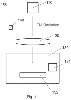
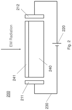
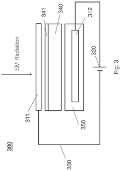
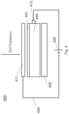
- The system comprises an electromagnetic radiation source, an optical assembly, and an exposure chamber with a substrate support and an electrode assembly that applies an electric field to an EM-sensitive layer on the semiconductor substrate during exposure to EUV radiation.
Methods and apparatus to reduce extreme ultraviolet light for photolithography
PatentPendingEP4625049A1
Innovation
- Employing a dual-dose exposure method using both UV and EUV light to sensitize the photoresist, reducing the EUV light dose needed for patterning by altering the solubility characteristics of the photoresist, thereby lowering energy and equipment costs.


Supply Chain Dependencies in EUV Systems
The EUV lithography supply chain represents one of the most complex and concentrated ecosystems in the semiconductor industry, creating significant dependencies that directly impact cost efficiency in non-volatile memory production. ASML holds a monopolistic position as the sole supplier of EUV scanners, creating an unprecedented bottleneck that affects the entire industry's production capacity and pricing dynamics.
Critical component dependencies extend beyond the scanner itself to encompass specialized subsystems that require unique manufacturing capabilities. The EUV light source relies on laser-produced plasma technology, with Cymer serving as the primary supplier of drive laser systems. These high-power CO2 lasers must achieve precise timing and power delivery, creating dependencies on specialized optical components and control systems that have limited alternative suppliers.
Mirror manufacturing represents another critical dependency, as EUV mirrors require multilayer coatings with sub-nanometer precision. Only a handful of suppliers worldwide possess the capability to produce these mirrors at the required quality levels, including Zeiss and specialized coating facilities. The extreme precision requirements and lengthy qualification processes make supplier diversification extremely challenging.
Photoresist materials for EUV lithography constitute a particularly acute supply chain vulnerability. The chemical complexity and performance requirements have limited the number of qualified suppliers to primarily JSR, Tokyo Ohka Kogyo, and Shin-Etsu Chemical. The development timeline for new photoresist formulations spans multiple years, creating long-term dependencies that directly impact production costs and scalability.
Pellicle technology, essential for protecting reticles from contamination, remains in development with limited supplier options. The absence of reliable pellicles increases reticle replacement costs and impacts yield, creating additional cost pressures in memory production. This dependency affects both capital expenditure planning and operational cost structures.
The geographic concentration of suppliers, primarily in Europe, Japan, and limited facilities in other regions, creates additional risks related to geopolitical tensions, natural disasters, and transportation disruptions. These dependencies necessitate strategic inventory management and long-term supply agreements that impact working capital requirements and overall cost efficiency in memory manufacturing operations.
Economic Impact of EUV Adoption in NVM
The adoption of EUV lithography in non-volatile memory production represents a significant economic paradigm shift that extends far beyond initial capital expenditure considerations. The technology's economic impact manifests through multiple interconnected dimensions that fundamentally alter the cost structure and competitive dynamics within the NVM industry.
Capital investment requirements for EUV implementation create substantial barriers to entry, with individual EUV scanners costing approximately $200-300 million each. Leading memory manufacturers like Samsung, SK Hynix, and Micron have committed multi-billion dollar investments to establish EUV-capable production lines. This massive capital intensity consolidates market power among established players while potentially excluding smaller competitors from advanced node manufacturing.
The economic benefits of EUV adoption become apparent through manufacturing efficiency gains and yield improvements. Traditional multi-patterning techniques required for advanced nodes without EUV involve complex process flows with 15-20 lithography steps, compared to 3-5 steps with EUV. This reduction translates to significant operational cost savings, decreased cycle times, and improved manufacturing throughput. Industry data suggests that EUV implementation can reduce overall lithography costs by 20-30% for sub-10nm nodes despite higher equipment costs.
Production scalability represents another critical economic dimension. EUV enables manufacturers to achieve higher transistor densities and improved performance characteristics in NVM devices, directly impacting product pricing power and market positioning. The technology facilitates the production of next-generation storage solutions with enhanced capacity and speed, commanding premium pricing in enterprise and consumer markets.
Supply chain economics undergo transformation as EUV adoption creates new dependencies and cost structures. The limited number of EUV equipment suppliers, primarily ASML, introduces supply chain concentration risks while driving collaborative relationships between memory manufacturers and equipment providers. Long-term service agreements and technology roadmap alignment become essential economic considerations.
The broader economic impact extends to regional competitiveness and technological sovereignty. Nations and regions investing heavily in EUV-capable manufacturing infrastructure gain strategic advantages in the global semiconductor value chain, influencing trade dynamics and technology leadership positions in the critical memory sector.
Unlock deeper insights with Patsnap Eureka Quick Research — get a full tech report to explore trends and direct your research. Try now!
Generate Your Research Report Instantly with AI Agent
Supercharge your innovation with Patsnap Eureka AI Agent Platform!