

EUV Lithography vs Optical Proximity Correction: Performance Trade-offs
APR 2, 20268 MIN READ
Generate Your Research Report Instantly with AI Agent
PatSnap Eureka helps you evaluate technical feasibility & market potential.
EUV Lithography Development Background and OPC Integration Goals
Extreme Ultraviolet (EUV) lithography emerged as a revolutionary semiconductor manufacturing technology following decades of intensive research and development. The technology utilizes 13.5 nm wavelength light, significantly shorter than the 193 nm wavelength used in conventional deep ultraviolet (DUV) lithography. This fundamental shift was driven by the semiconductor industry's relentless pursuit of Moore's Law, as traditional optical lithography approached its physical limits around the 22 nm technology node.
The development trajectory of EUV lithography began in the 1980s with initial research into soft X-ray projection lithography. By the 1990s, major semiconductor manufacturers and equipment suppliers recognized EUV as the most promising next-generation lithography solution. The technology faced numerous technical challenges, including the development of reflective optics systems, high-power EUV light sources, and specialized photoresist materials capable of responding to EUV radiation.
EUV lithography's shorter wavelength theoretically enables superior resolution capabilities compared to DUV systems, potentially reducing the complexity of multiple patterning techniques. However, the transition to EUV has necessitated a fundamental reevaluation of Optical Proximity Correction strategies. Traditional OPC techniques, optimized for DUV wavelengths, required substantial modifications to address EUV-specific phenomena such as mask three-dimensional effects, flare, and stochastic variations.
The integration goals for EUV lithography and OPC encompass several critical objectives. Primary among these is achieving consistent critical dimension control across varying pattern densities and geometries while maintaining acceptable throughput levels. The technology aims to enable single-exposure patterning for advanced nodes, reducing manufacturing complexity and cost compared to multi-patterning DUV approaches.
Another crucial integration goal involves optimizing the trade-off between resolution enhancement and computational complexity. EUV-specific OPC models must account for unique physical effects while remaining computationally tractable for full-chip implementations. This requires developing sophisticated correction algorithms that can handle EUV's distinct imaging characteristics, including enhanced sensitivity to mask topography and localized dose variations.
The ultimate objective is establishing a robust, high-volume manufacturing process that leverages EUV's inherent resolution advantages while mitigating its current limitations through advanced OPC techniques, thereby enabling continued semiconductor scaling.
Market Demand for Advanced Semiconductor Manufacturing Solutions
The global semiconductor industry faces unprecedented demand for advanced manufacturing solutions as device scaling approaches fundamental physical limits. The transition to extreme ultraviolet lithography represents a critical inflection point, driven by the industry's relentless pursuit of smaller feature sizes below 7nm technology nodes. This demand stems from multiple converging factors including artificial intelligence acceleration, high-performance computing requirements, and the proliferation of advanced mobile processors requiring enhanced computational density.
Market dynamics reveal a complex landscape where traditional optical lithography approaches encounter increasing limitations. The semiconductor manufacturing ecosystem demonstrates growing appetite for solutions that can deliver sub-10nm patterning capabilities while maintaining economic viability. Leading foundries and integrated device manufacturers actively seek technologies that balance resolution enhancement with manufacturing throughput, creating substantial market opportunities for both EUV lithography systems and sophisticated optical proximity correction methodologies.
The automotive electronics revolution, particularly in autonomous driving and electric vehicle applications, generates additional demand for advanced semiconductor manufacturing capabilities. These applications require processors with enhanced performance characteristics that can only be achieved through cutting-edge lithography techniques. Similarly, the expansion of 5G infrastructure and edge computing applications creates sustained demand for high-performance semiconductors manufactured using the most advanced available processes.
Enterprise and cloud computing markets drive significant demand for memory and logic devices requiring the finest achievable feature sizes. Data center processors, graphics processing units, and specialized AI accelerators represent high-value applications where the performance benefits of advanced lithography justify substantial manufacturing investments. The market demonstrates willingness to absorb higher costs associated with next-generation lithography solutions when they enable meaningful performance improvements.
The competitive landscape reveals that semiconductor manufacturers face increasing pressure to differentiate their offerings through superior performance characteristics achievable only through advanced manufacturing processes. This creates a self-reinforcing cycle where market demand for high-performance devices drives adoption of sophisticated lithography solutions, which in turn enables new applications and market opportunities that further increase demand for advanced manufacturing capabilities.
Current EUV-OPC Implementation Challenges and Technical Barriers
The integration of EUV lithography with optical proximity correction presents significant implementation challenges that stem from the fundamental differences between EUV and traditional DUV systems. The shorter wavelength of EUV light at 13.5 nm creates unique optical phenomena that existing OPC models struggle to accurately predict and compensate for.
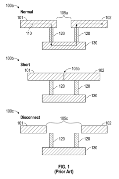
Mask three-dimensional effects represent one of the most critical barriers in EUV-OPC implementation. Unlike DUV systems where masks can be treated as thin absorbers, EUV masks exhibit substantial 3D topographical effects due to the multilayer reflective structure and absorber thickness. These effects cause shadowing, telecentricity errors, and non-uniform imaging across the exposure field, making traditional OPC correction algorithms insufficient for accurate pattern prediction.
Stochastic effects pose another fundamental challenge that distinguishes EUV from conventional lithography. The limited number of photons available in EUV exposure creates statistical variations in photon absorption, leading to line edge roughness, line width roughness, and stochastic defects. Current OPC models lack robust frameworks to incorporate these probabilistic effects, resulting in unpredictable pattern fidelity that cannot be adequately corrected through conventional proximity correction techniques.
The computational complexity of EUV-OPC modeling presents significant technical barriers. Accurate simulation of EUV imaging requires rigorous electromagnetic field calculations that account for mask topography, multilayer reflectivity variations, and oblique incidence effects. These computationally intensive models dramatically increase OPC runtime, making full-chip correction impractical with existing computational resources and algorithms.
Resist modeling challenges further complicate EUV-OPC implementation. EUV resists exhibit different photochemical behavior compared to DUV materials, including secondary electron effects and acid diffusion characteristics that vary with local pattern density. The lack of mature resist models specifically calibrated for EUV processes limits the accuracy of OPC predictions and corrections.
Source mask optimization integration with EUV systems faces unique constraints due to the limited availability of EUV illumination source configurations and the complex interaction between source pupil shapes and mask 3D effects. Traditional SMO algorithms require substantial modification to accommodate these EUV-specific constraints while maintaining acceptable correction accuracy and manufacturing feasibility.
Current EUV-OPC Integration and Optimization Approaches
01 EUV mask optimization and defect mitigation techniques
Extreme ultraviolet lithography requires specialized mask designs and defect correction methods to achieve optimal pattern transfer. Advanced techniques focus on mask blank preparation, multilayer reflective coatings, and defect inspection methodologies. These approaches address the unique challenges of EUV wavelengths including absorption effects and phase shift management to ensure high-fidelity pattern reproduction on wafers.- EUV mask optimization and defect mitigation techniques: Extreme ultraviolet lithography requires specialized mask designs and defect correction methods to achieve optimal pattern transfer. Advanced techniques focus on mask blank preparation, multilayer reflective coatings, and defect inspection methodologies. These approaches address the unique challenges of EUV wavelengths including absorption effects and phase shift management to ensure high-fidelity pattern reproduction on wafers.
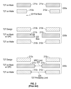
- Model-based optical proximity correction algorithms: Computational methods are employed to predict and compensate for optical diffraction effects that cause pattern distortions during lithography. These algorithms utilize physical models of the imaging system to calculate necessary adjustments to mask geometries. The correction process involves iterative simulations that account for light interference patterns, resist behavior, and process variations to achieve target dimensions on the substrate.
- Sub-resolution assist features and pattern decomposition: Enhancement techniques involve adding non-printing features to masks that improve the imaging of primary patterns without being resolved themselves. Pattern decomposition strategies split complex layouts into multiple exposure steps to overcome resolution limitations. These methods optimize the placement and sizing of auxiliary structures based on proximity effects and process window requirements to extend lithographic capabilities beyond conventional limits.
- Source-mask co-optimization for lithography enhancement: Simultaneous optimization of illumination source configurations and mask patterns provides superior imaging performance compared to sequential optimization approaches. This methodology explores the combined design space to identify optimal pairings that maximize process margins and pattern fidelity. The technique addresses the interdependencies between source shapes, mask features, and imaging characteristics to achieve enhanced resolution and depth of focus.
- Machine learning and inverse lithography technology: Advanced computational approaches utilize artificial intelligence and inverse problem-solving methods to generate optimal mask solutions directly from target patterns. These techniques bypass traditional rule-based corrections by learning from large datasets or employing optimization algorithms that work backward from desired wafer results. The methods can handle complex two-dimensional pattern interactions and provide solutions that conventional approaches may not discover.
02 Optical proximity correction algorithms for sub-wavelength features
Computational methods are employed to compensate for optical diffraction effects that occur when feature sizes approach or fall below the exposure wavelength. These correction algorithms modify mask patterns by adding sub-resolution assist features, adjusting edge positions, and optimizing feature shapes. The techniques enable accurate reproduction of intended circuit patterns despite physical limitations of the optical system.Expand Specific Solutions03 Model-based lithography simulation and verification
Predictive modeling systems simulate the complete lithography process including illumination, mask interaction, projection optics, and resist behavior. These models enable pre-manufacturing verification of pattern fidelity and identification of potential printing issues. Advanced simulation frameworks incorporate physical and chemical effects to accurately predict final wafer patterns and guide mask design optimization.Expand Specific Solutions04 Source-mask co-optimization techniques
Integrated optimization approaches simultaneously adjust both illumination source characteristics and mask patterns to maximize lithographic performance. These methods explore the combined design space of pupil fill patterns, polarization states, and mask geometries. The co-optimization strategy achieves superior process windows and pattern fidelity compared to sequential optimization of individual components.Expand Specific Solutions05 Resolution enhancement through advanced mask technologies
Novel mask structures and materials improve resolution capabilities beyond conventional approaches. These technologies include phase-shifting masks, attenuated masks, and chromeless phase lithography configurations. Enhanced mask designs manipulate the phase and amplitude of transmitted or reflected light to generate constructive and destructive interference patterns that improve feature resolution and contrast.Expand Specific Solutions
Major Semiconductor Equipment and EDA Tool Vendors Analysis
The EUV lithography versus optical proximity correction competitive landscape reflects a mature semiconductor manufacturing industry experiencing rapid technological evolution driven by advanced node requirements. The market demonstrates significant scale with established players like ASML Netherlands BV dominating EUV equipment supply, while foundries including Taiwan Semiconductor Manufacturing Co., Samsung Electronics, and Intel Corp. represent major technology adopters. Chinese manufacturers such as SMIC and Shanghai Huali are aggressively pursuing advanced capabilities. Technology maturity varies considerably - EUV lithography has reached production readiness at leading fabs for sub-7nm processes, while OPC techniques continue evolving through companies like D2S and Siemens Industry Software to address complex patterning challenges. Equipment suppliers including Applied Materials, Tokyo Electron, and Lam Research provide complementary processing solutions, while research institutions like MIT and Imec drive next-generation innovations, creating a dynamic ecosystem balancing cutting-edge EUV adoption with sophisticated computational lithography approaches.
Taiwan Semiconductor Manufacturing Co., Ltd.
Technical Solution: TSMC has developed comprehensive EUV lithography implementation strategies for their advanced process nodes, utilizing ASML's EUV systems with proprietary OPC methodologies. Their approach involves multi-patterning techniques combined with EUV single exposure for critical layers, achieving line edge roughness below 2nm for 3nm and 5nm processes. TSMC's OPC solutions incorporate machine learning algorithms to predict and compensate for process variations, including EUV stochastic effects and mask shadowing. The company has successfully demonstrated EUV lithography for contact holes and metal layers while maintaining traditional optical lithography with advanced OPC for less critical features, optimizing cost-performance trade-offs across different process steps.
Strengths: Industry-leading high-volume EUV manufacturing experience with proven yield optimization and cost-effective hybrid lithography approaches. Weaknesses: Heavy dependence on ASML equipment supply and significant capital investment requirements for EUV infrastructure expansion.
ASML Netherlands BV
Technical Solution: ASML is the world's leading supplier of EUV lithography systems, with their TWINSCAN NXE series achieving 13.5nm wavelength exposure capabilities. Their EUV systems deliver high-resolution patterning for advanced nodes below 7nm, enabling critical dimension uniformity within 2nm across 300mm wafers. The company integrates sophisticated optical proximity correction algorithms directly into their lithography exposure tools, optimizing mask data preparation and real-time pattern correction during exposure. ASML's computational lithography solutions include advanced OPC modeling that accounts for EUV-specific effects such as stochastic variations and mask 3D effects, providing comprehensive process window optimization for sub-3nm manufacturing nodes.
Strengths: Market leadership in EUV technology with proven high-volume manufacturing capability and integrated OPC solutions. Weaknesses: Extremely high capital costs and complex maintenance requirements limiting accessibility to only the largest semiconductor manufacturers.
Core Patents in EUV Source Mask Optimization Technologies
Methods for optical proximity correction in the design and fabrication of integrated circuits using extreme ultraviolet lithography
PatentActiveUS9651855B2
Innovation
- The implementation of novel optical proximity correction (OPC) techniques that generate a third polygon with dimensions corresponding to the combination of first and second design polygons and a filled polygon within it, allowing for closer tip proximity without the need for multiple masks.
Lithography simulation and optical proximity correction
PatentWO2021061277A1
Innovation
- The implementation of field-guided post-exposure bake parameters in OPC models, including anisotropic acid etching, ion, electron, and hole movement characteristics, to generate improved OPC models for mask design and substrate patterning, utilizing an electric field to control acid distribution and enhance resist deprotection.


Semiconductor Industry Standards and Export Control Regulations
The semiconductor industry operates under a complex framework of international standards and export control regulations that significantly impact the development and deployment of advanced lithography technologies, including EUV lithography and optical proximity correction systems. These regulatory frameworks are designed to balance technological advancement with national security considerations, creating a multi-layered compliance environment for semiconductor manufacturers.
International standards organizations such as SEMI, IEEE, and ISO establish technical specifications that govern the performance, safety, and interoperability requirements for semiconductor manufacturing equipment. For EUV lithography systems, these standards address critical parameters including exposure dose uniformity, overlay accuracy, and contamination control protocols. The stringent requirements often necessitate trade-offs between system performance and regulatory compliance, particularly in areas of radiation safety and environmental protection.
Export control regulations, primarily governed by the Wassenaar Arrangement and implemented through national frameworks like the U.S. Export Administration Regulations (EAR) and European Union dual-use regulations, impose significant restrictions on the transfer of advanced lithography technologies. These controls specifically target EUV systems and sophisticated OPC software due to their strategic importance in producing cutting-edge semiconductors for defense and critical infrastructure applications.
The regulatory landscape creates particular challenges for OPC technology development, as advanced computational algorithms and machine learning techniques used in modern OPC solutions may fall under software export restrictions. Companies must navigate complex licensing requirements when developing or deploying AI-enhanced OPC systems across international boundaries, potentially limiting collaborative research and development efforts.
Compliance costs associated with these regulations can substantially impact the total cost of ownership for advanced lithography systems. Manufacturers must invest in specialized compliance infrastructure, undergo regular audits, and maintain detailed documentation of technology transfers. These requirements often influence the design choices between EUV and advanced OPC solutions, as companies weigh performance benefits against regulatory complexity and associated costs in their strategic technology roadmaps.
Cost-Performance Analysis Framework for EUV-OPC Trade-offs
The cost-performance analysis framework for EUV-OPC trade-offs requires a comprehensive evaluation methodology that balances capital expenditure, operational costs, and manufacturing performance metrics. This framework establishes quantitative benchmarks for decision-making between extreme ultraviolet lithography adoption and enhanced optical proximity correction implementations.
Capital expenditure analysis forms the foundation of this framework, encompassing EUV scanner acquisition costs ranging from $180-200 million per tool, compared to ArF immersion systems at $40-60 million with advanced OPC software investments of $5-15 million. The framework incorporates total cost of ownership calculations including infrastructure modifications, cleanroom upgrades, and specialized maintenance requirements for EUV systems.
Operational cost modeling addresses consumables, throughput variations, and yield implications. EUV systems demonstrate lower mask costs per layer but higher photoresist expenses and power consumption. The framework quantifies these variables through cost-per-wafer metrics, factoring in EUV source availability typically ranging 80-90% versus 95%+ for mature optical systems with sophisticated OPC.
Performance metrics integration encompasses resolution capabilities, pattern fidelity, and process window characteristics. The framework establishes normalized performance indices comparing EUV's native 13.5nm wavelength advantages against multi-patterning OPC solutions. Critical dimension uniformity, line edge roughness, and overlay accuracy serve as key performance indicators within the analytical model.
Risk assessment components evaluate technology maturity levels, supply chain dependencies, and scalability factors. EUV technology carries higher implementation risks due to limited supplier ecosystems and evolving infrastructure requirements, while OPC-based approaches leverage established manufacturing ecosystems with predictable cost structures.
The framework incorporates sensitivity analysis for various production scenarios, node requirements, and volume projections. Break-even calculations determine optimal technology selection based on production volumes, typically favoring EUV for high-volume advanced node manufacturing exceeding 10,000 wafers per month, while OPC solutions remain cost-effective for lower volumes or mature node applications.
Unlock deeper insights with PatSnap Eureka Quick Research — get a full tech report to explore trends and direct your research. Try now!
Generate Your Research Report Instantly with AI Agent
Supercharge your innovation with PatSnap Eureka AI Agent Platform!