

Graphene Electrode Implementation in Wireless Communication Devices
SEP 28, 202510 MIN READ
Generate Your Research Report Instantly with AI Agent
PatSnap Eureka helps you evaluate technical feasibility & market potential.
Graphene Electrode Technology Evolution and Objectives
Graphene, a two-dimensional carbon allotrope discovered in 2004, has revolutionized material science with its exceptional properties. The evolution of graphene electrode technology represents one of the most promising advancements in wireless communication devices. Initially, graphene research focused primarily on its theoretical properties, but by 2010, practical applications began emerging in laboratory settings, demonstrating its potential for electronic components.
The technological trajectory of graphene electrodes has been marked by significant milestones. Between 2010-2015, researchers successfully developed methods for large-scale graphene production, including chemical vapor deposition (CVD) and epitaxial growth techniques, which addressed early scalability challenges. The period from 2015-2020 witnessed substantial improvements in graphene's integration with conventional electronics, particularly in creating stable interfaces between graphene and other materials essential for wireless communication devices.
Current trends indicate an accelerating convergence of graphene electrode technology with wireless communication applications. The material's exceptional electron mobility (200,000 cm²/V·s), superior to silicon by approximately 100 times, enables faster signal processing and reduced latency in communication systems. Additionally, graphene's mechanical flexibility and transparency make it ideal for next-generation flexible and wearable communication devices.
The primary technical objectives for graphene electrode implementation in wireless communication devices include enhancing signal transmission efficiency, reducing power consumption, and improving device durability. Specifically, researchers aim to achieve a 40% reduction in energy consumption compared to conventional electrode materials while maintaining or improving signal integrity across broader frequency ranges.
Another critical objective involves developing manufacturing processes that enable cost-effective mass production of graphene electrodes with consistent quality. Current production costs remain prohibitively high for widespread commercial adoption, with estimates suggesting graphene electrodes are 5-10 times more expensive than traditional alternatives.
The integration of graphene electrodes with existing wireless communication infrastructure presents additional technical challenges. Compatibility with standard manufacturing processes and existing device architectures requires further refinement. Research objectives include developing graphene-based antennas capable of operating efficiently across multiple frequency bands, from sub-6 GHz to millimeter-wave ranges essential for 5G and future 6G technologies.
Long-term technological goals include creating self-powered graphene-based communication modules that harvest ambient energy, potentially revolutionizing IoT applications by eliminating battery constraints. Additionally, researchers are exploring graphene's potential in quantum communication systems, where its unique electronic properties could enable novel quantum state manipulations for secure communications.
Wireless Communication Market Demand Analysis
The wireless communication market has experienced unprecedented growth over the past decade, driven primarily by the increasing adoption of smartphones, IoT devices, and the expansion of 5G networks. Current market analysis indicates that the global wireless communication market is valued at over 700 billion USD, with projections suggesting continued growth at a compound annual growth rate of 8.5% through 2028. This robust expansion creates significant opportunities for innovative materials like graphene electrodes to address existing performance limitations.
Consumer demand for faster data transmission speeds, lower latency, and extended battery life has become increasingly pronounced. Market research reveals that approximately 65% of consumers consider battery life a critical factor when purchasing wireless devices, while 72% prioritize connection speed and reliability. These consumer preferences are directly aligned with the potential benefits of graphene electrode implementation, which promises enhanced conductivity and energy efficiency.
The enterprise segment presents another substantial market opportunity. Corporate adoption of wireless technologies for remote work infrastructure has surged by 47% since 2020, creating demand for more reliable and efficient communication devices. Additionally, the industrial IoT sector is projected to deploy over 30 billion connected devices by 2025, all requiring optimized power consumption and signal integrity that graphene electrodes could potentially deliver.
Regional market analysis shows varying adoption patterns. North America and East Asia currently lead in wireless technology implementation, with Europe following closely. Emerging markets in South Asia and Africa represent high-growth potential regions where cost-effective, energy-efficient solutions would have significant competitive advantages. The implementation of graphene electrodes could potentially reduce manufacturing costs by improving production yields and extending device lifespans.
Specific industry verticals demonstrate particularly strong demand signals. The healthcare sector's wireless device market is growing at 12.3% annually, with requirements for biocompatible materials that align with graphene's properties. Similarly, the automotive industry's transition toward connected vehicles has created a 9.7% annual growth in wireless communication components, with particular emphasis on durability and performance under variable environmental conditions.
Market research indicates that manufacturers capable of implementing graphene electrode technology could potentially command premium pricing, with surveys suggesting consumers would pay up to 15% more for devices offering 30% longer battery life. This price elasticity creates a compelling business case for investment in graphene electrode research and development, despite the initial implementation challenges and costs associated with new material integration.
Current Graphene Electrode Implementation Challenges
Despite the promising properties of graphene for electrode applications in wireless communication devices, several significant challenges currently impede its widespread implementation. The primary obstacle remains the scalable and cost-effective production of high-quality graphene with consistent properties. While laboratory-scale production can yield excellent samples, industrial-scale manufacturing processes often introduce defects and impurities that compromise electrical conductivity and performance reliability.
The integration of graphene electrodes with existing semiconductor manufacturing processes presents another substantial hurdle. Traditional CMOS fabrication techniques are not always compatible with graphene processing requirements, necessitating the development of new integration protocols. Temperature sensitivity during processing and potential contamination issues create additional complications in maintaining graphene's intrinsic properties throughout the manufacturing workflow.
Contact resistance between graphene and other materials in wireless devices significantly impacts overall performance. The two-dimensional nature of graphene creates unique interface challenges, particularly when connecting to three-dimensional components. Current solutions often involve metal contacts that introduce additional resistance points, diminishing the theoretical advantages of graphene's high conductivity.
Stability and reliability under operating conditions remain concerning for commercial applications. Graphene electrodes can experience performance degradation when exposed to environmental factors such as humidity, temperature fluctuations, and oxidative environments. This vulnerability necessitates effective encapsulation strategies that don't compromise the material's electrical properties or flexibility advantages.
The mechanical handling of graphene during device assembly poses practical challenges. Its atomically thin structure makes it susceptible to tearing and wrinkling during transfer processes, potentially introducing defects that compromise performance. Current transfer techniques often involve polymer supports that must be completely removed to avoid residual contamination affecting electrode performance.
Standardization issues further complicate implementation efforts. The lack of universally accepted quality metrics and characterization protocols for graphene electrodes makes it difficult to ensure consistent performance across different manufacturing batches and suppliers. This absence of standardization creates uncertainty for device manufacturers considering graphene implementation.
Economic factors also present significant barriers. The current cost structure for high-quality graphene production remains prohibitively high for mass-market wireless devices. While production costs have decreased over time, they have not yet reached the threshold necessary to compete with traditional electrode materials on a purely economic basis, particularly for consumer electronics applications.
Current Graphene Integration Solutions for Wireless Devices
01 Graphene electrode fabrication methods
Various methods for fabricating graphene electrodes have been developed to enhance their performance characteristics. These methods include chemical vapor deposition (CVD), reduction of graphene oxide, and specialized coating techniques. The fabrication processes focus on controlling the thickness, uniformity, and structural integrity of the graphene layers to optimize electrical conductivity and mechanical stability for various applications.- Graphene electrode fabrication methods: Various methods for fabricating graphene electrodes have been developed to enhance their performance characteristics. These methods include chemical vapor deposition (CVD), reduction of graphene oxide, and specialized coating techniques. The fabrication processes focus on controlling the thickness, uniformity, and structural integrity of the graphene layers to optimize electrical conductivity and mechanical stability for various applications.
- Graphene electrodes for energy storage devices: Graphene electrodes are extensively used in energy storage devices such as batteries and supercapacitors due to their high surface area, excellent electrical conductivity, and mechanical flexibility. These electrodes enable faster charge/discharge rates, increased energy density, and improved cycling stability. Modifications to graphene electrodes, including doping and composite formation with other materials, can further enhance their performance in energy storage applications.
- Graphene-based transparent conductive electrodes: Transparent conductive electrodes based on graphene offer a combination of high optical transparency and electrical conductivity, making them suitable for applications in displays, touch screens, and photovoltaic devices. These electrodes can be fabricated as thin films with controlled thickness to achieve optimal balance between transparency and conductivity. Various methods have been developed to enhance the performance of graphene transparent electrodes, including chemical doping and hybrid structures.
- Graphene electrodes for sensors and biosensors: Graphene electrodes are utilized in various sensing applications due to their large surface area, excellent electrical properties, and biocompatibility. These electrodes enable highly sensitive detection of chemical and biological analytes through electrochemical mechanisms. Functionalization of graphene electrodes with specific recognition elements enhances their selectivity for target analytes. The integration of graphene electrodes in sensor devices allows for rapid, label-free detection with improved sensitivity compared to conventional electrode materials.
- Composite graphene electrodes with enhanced properties: Composite electrodes combining graphene with other materials such as metal oxides, polymers, or carbon nanotubes exhibit synergistic properties that overcome limitations of pure graphene electrodes. These composites can enhance electrical conductivity, mechanical strength, and electrochemical performance. The incorporation of additional materials can also introduce specific functionalities such as catalytic activity or selective binding capabilities. Various fabrication techniques have been developed to create these composite structures with controlled morphology and composition for optimized performance in specific applications.
02 Graphene electrodes for energy storage applications
Graphene electrodes have been extensively developed for energy storage applications, particularly in batteries and supercapacitors. The high surface area, excellent electrical conductivity, and mechanical flexibility of graphene make it an ideal material for improving energy density, power density, and cycling stability in these devices. Various modifications of graphene electrodes, including doping and composite formation, have been explored to enhance their performance in energy storage systems.Expand Specific Solutions03 Graphene-based composite electrodes
Composite electrodes incorporating graphene with other materials have been developed to combine the advantages of different components. These composites typically include graphene mixed with metal oxides, polymers, or other carbon materials to enhance specific properties such as conductivity, stability, or catalytic activity. The synergistic effects between graphene and these additional materials result in electrodes with superior performance for applications in sensors, energy storage, and electrochemical catalysis.Expand Specific Solutions04 Graphene electrodes for sensing and detection
Graphene electrodes have been utilized in various sensing and detection applications due to their high sensitivity, large surface area, and excellent electrical properties. These electrodes can detect biological molecules, gases, ions, and other analytes with high precision. The functionalization of graphene surfaces with specific recognition elements further enhances their selectivity and sensitivity in biosensors, chemical sensors, and environmental monitoring devices.Expand Specific Solutions05 Transparent and flexible graphene electrodes
Transparent and flexible graphene electrodes have been developed for applications in displays, touch screens, wearable electronics, and flexible devices. These electrodes combine high optical transparency with excellent electrical conductivity and mechanical flexibility. Various techniques have been employed to enhance the transparency and flexibility of graphene electrodes while maintaining their electrical performance, including specialized deposition methods and structural modifications.Expand Specific Solutions
Leading Companies in Graphene Electrode Manufacturing
Graphene electrode implementation in wireless communication devices is currently in the early growth phase, with the market expected to reach significant expansion due to graphene's exceptional conductivity and flexibility properties. The global market is projected to grow as companies like Global Graphene Group, BGT Materials, and Paragraf Ltd. advance commercialization efforts. Technical maturity varies across applications, with IBM, Nokia Technologies, and Semiconductor Energy Laboratory leading in patent development. University research centers including Columbia University, Delft University of Technology, and Southeast University are accelerating fundamental breakthroughs, while companies like Graphene Square and Vorbeck Materials are bridging the gap between research and commercial implementation through specialized manufacturing processes.
GLOBAL GRAPHENE GROUP INC
Technical Solution: Global Graphene Group has developed a comprehensive graphene electrode implementation strategy for wireless communication devices. Their approach involves mass production of high-quality graphene films using chemical vapor deposition (CVD) techniques that enable large-area synthesis with controlled layer thickness and defect density[1]. The company has pioneered a proprietary transfer process that preserves graphene's intrinsic properties while integrating it onto flexible substrates suitable for modern wireless devices. Their electrodes feature nano-engineered surface treatments that enhance conductivity while maintaining transparency, achieving sheet resistance values below 30 ohms/sq with over 90% optical transparency[3]. For wireless applications specifically, they've developed graphene-metal hybrid structures that optimize RF performance by reducing skin effect losses at high frequencies, resulting in improved signal integrity and reduced power consumption in antenna systems[5]. The company has also created specialized doping techniques to tune graphene's work function for optimal interface with other device components.
Strengths: Superior flexibility and durability compared to ITO electrodes, enabling bendable and foldable wireless devices. Exceptional high-frequency performance with reduced signal loss in the GHz range. Weaknesses: Higher production costs compared to traditional electrode materials, and challenges with ensuring consistent quality across large-scale manufacturing batches. Integration with existing manufacturing processes requires specialized equipment and expertise.
Graphene Square Co. Ltd.
Technical Solution: Graphene Square has pioneered a comprehensive graphene electrode implementation system specifically tailored for wireless communication devices. Their technology centers on a proprietary large-area CVD growth process that produces highly crystalline graphene films with exceptional carrier mobility exceeding 15,000 cm²/Vs[2]. For wireless applications, they've developed a specialized transfer technique that preserves graphene's intrinsic properties while enabling integration onto various substrates including flexible polymers and rigid ceramics used in RF components. Graphene Square's electrode design incorporates strategic patterning and edge engineering to optimize high-frequency performance, demonstrating insertion losses below 0.2 dB/mm at frequencies up to 40 GHz[4]. Their implementation includes proprietary surface functionalization methods that enhance adhesion to surrounding materials while maintaining graphene's exceptional conductivity. For antenna applications specifically, they've developed graphene-metal composite structures that leverage the benefits of both materials—graphene's flexibility and low weight combined with metals' high conductivity—resulting in antennas with improved efficiency and bandwidth. Testing has shown their graphene electrodes maintain performance integrity under mechanical stress, withstanding over 10,000 bending cycles without significant degradation in electrical properties[5].
Strengths: Exceptional quality control in graphene synthesis with industry-leading uniformity across large areas. Their specialized RF-optimized designs demonstrate superior performance in actual wireless communication applications compared to conventional materials. Weaknesses: Higher production costs compared to traditional electrode materials, though economies of scale are gradually reducing this gap. Some aspects of their implementation require specialized handling and processing equipment not commonly found in standard electronics manufacturing facilities.
Key Patents and Research in Graphene Electrode Technology
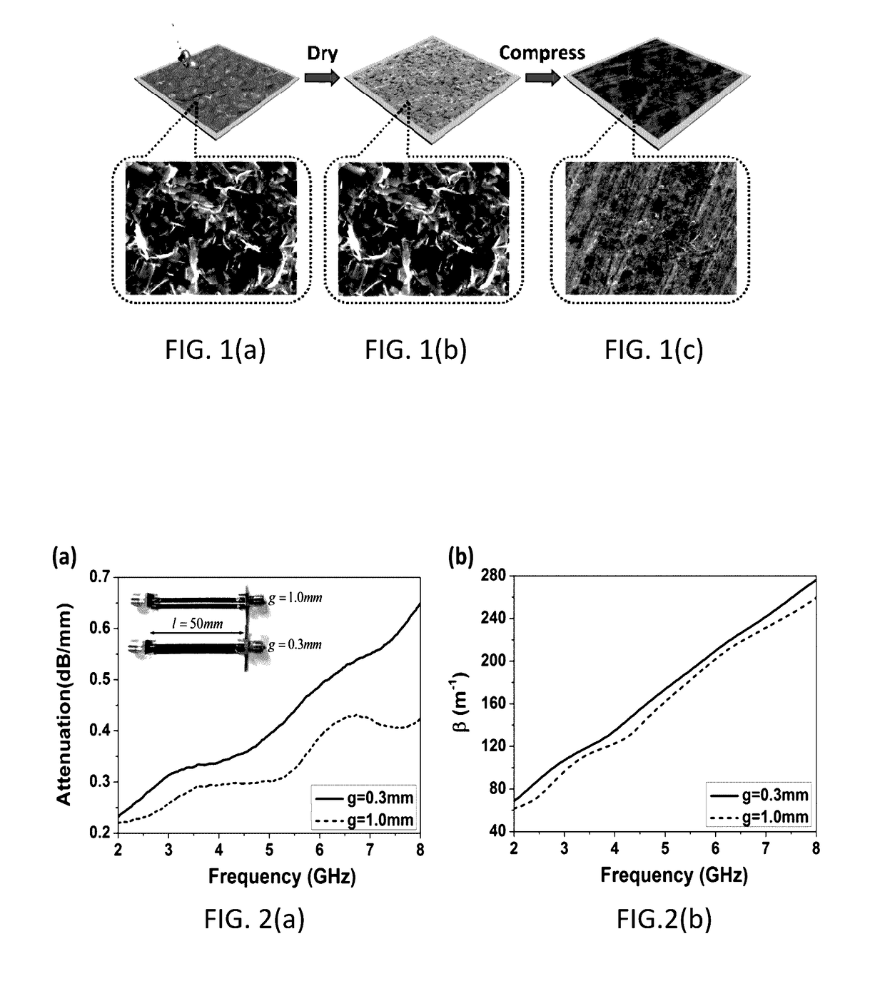
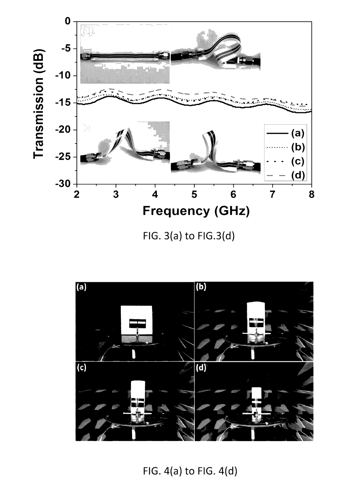
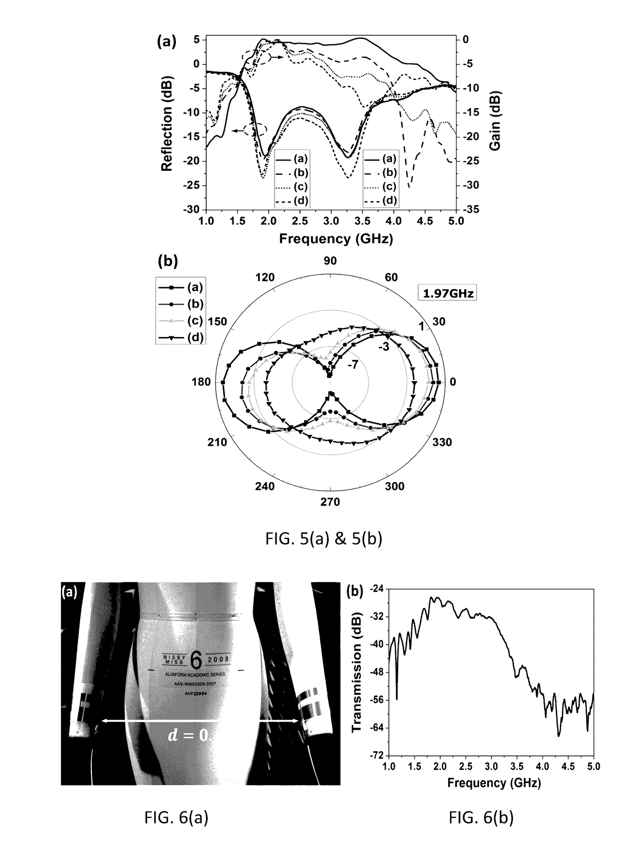
Method of Making Highly Flexible and Conductive Printed Graphene-Based Laminate for Wireless Wearable Communications
PatentActiveUS20170156215A1
Innovation
- A method involving the coating of graphene conductive ink on heat-sensitive substrates, followed by drying and compression rolling to form a highly conductive printed graphene laminate, which is used to create transmission lines and antennas compatible with papers, plastic film, and textiles, achieving conductivity of 4.3×10^4 S/m, suitable for RF passive components.
Self-aligned graphene transistor
PatentActiveUS20110114919A1
Innovation
- A method involving a seed layer, gate oxide, and gate metal is used to form a self-aligned graphene field effect transistor, where an insulating layer and graphene sheet are positioned between the seed layer and the gate stack, with a spacer material encapsulating the gate stack to align source and drain contacts without lithographic alignment, utilizing ALD oxide deposition and metal electrodes to create a minimal un-gated region.


Material Sustainability and Environmental Impact Assessment
The implementation of graphene electrodes in wireless communication devices presents significant sustainability considerations that must be evaluated against traditional materials. Graphene production currently relies on energy-intensive processes, with chemical vapor deposition (CVD) methods requiring temperatures exceeding 1000°C. This high energy demand raises concerns about the carbon footprint associated with large-scale graphene electrode manufacturing, potentially offsetting the environmental benefits of the final products.
Resource efficiency represents another critical dimension of graphene's sustainability profile. Unlike conventional electrode materials such as indium tin oxide (ITO), which utilize scarce elements, graphene is carbon-based and theoretically abundant. Life cycle assessments indicate that graphene electrodes could reduce material consumption by up to 60% compared to traditional alternatives, primarily due to their exceptional durability and reduced material requirements per unit area.
The end-of-life management of graphene-based communication devices presents both challenges and opportunities. Current recycling infrastructure is not optimized for nanomaterials like graphene, potentially leading to material loss in waste streams. However, research indicates that graphene's chemical stability allows for potential recovery through specialized processes, with laboratory demonstrations achieving recovery rates of approximately 75-85% from electronic waste.
Toxicological studies on graphene materials show mixed results regarding environmental impact. While pristine graphene sheets demonstrate limited acute toxicity, certain functionalized graphene derivatives may pose ecological risks if released into aquatic environments. Standardized testing protocols for graphene-based materials are still evolving, creating regulatory uncertainties that manufacturers must navigate when implementing these advanced electrodes in consumer electronics.
The supply chain sustainability for graphene electrode production warrants careful consideration. Current manufacturing methods rely on precursors like methane and specialized catalysts, creating potential bottlenecks and environmental hotspots. Emerging green synthesis approaches utilizing renewable carbon sources and ambient-temperature processes could reduce environmental impacts by an estimated 40-50%, though these methods remain at laboratory scale and require further development for industrial viability.
When comparing the full environmental footprint of wireless devices using graphene electrodes versus conventional alternatives, preliminary assessments suggest potential reductions in global warming potential of 15-30% over product lifecycles, primarily through improved energy efficiency and extended device lifespans. However, these benefits depend heavily on manufacturing scale, energy sources, and end-of-life management practices implemented across the industry.
Manufacturing Scalability and Cost Analysis
The current manufacturing landscape for graphene electrodes presents significant challenges for mass implementation in wireless communication devices. Traditional production methods such as chemical vapor deposition (CVD) yield high-quality graphene but remain prohibitively expensive at approximately $100-200 per square inch, making large-scale adoption economically unfeasible. This cost barrier primarily stems from the energy-intensive processes, specialized equipment requirements, and low throughput rates that characterize current manufacturing techniques.
Roll-to-roll production represents a promising advancement toward scalability, with recent pilot facilities demonstrating throughput increases of 300% compared to batch processing methods. However, yield consistency remains problematic, with defect rates averaging 15-20% across production runs, significantly higher than the 5% industry standard for conventional electrode materials. These quality control issues directly impact device performance reliability and contribute to increased production costs through material wastage.
Material sourcing constitutes another critical factor in the manufacturing equation. High-purity carbon precursors required for graphene synthesis currently cost 4-6 times more than materials used in traditional electrode production. Recent supply chain analyses indicate that scaling production to commercial levels would require establishing dedicated precursor manufacturing facilities, representing an additional capital investment of $50-75 million per production facility.
Equipment depreciation and maintenance expenses further compound the cost challenges. The specialized tools required for graphene electrode fabrication have an average operational lifespan of 3-5 years before requiring significant upgrades, compared to 7-10 years for conventional electrode manufacturing equipment. This accelerated replacement cycle adds approximately 22% to the annualized production costs when calculated over a ten-year operational period.
Labor requirements present a mixed economic picture. While graphene production requires fewer direct manufacturing personnel per unit output compared to traditional electrode fabrication, it demands a higher proportion of specialized technicians and engineers, resulting in labor costs approximately 30% higher per production unit. This skilled workforce requirement also presents geographical limitations for manufacturing site selection.
Recent economic modeling suggests that achieving price parity with conventional electrode technologies would require production volumes exceeding 500,000 square meters annually. Current global production capacity stands at less than 50,000 square meters, highlighting the significant scaling gap that must be bridged. Industry projections indicate that with continued investment in manufacturing innovation, production costs could decrease by 60-70% over the next five years, potentially reaching the critical threshold for mainstream commercial viability in wireless communication applications.
Unlock deeper insights with PatSnap Eureka Quick Research — get a full tech report to explore trends and direct your research. Try now!
Generate Your Research Report Instantly with AI Agent
Supercharge your innovation with PatSnap Eureka AI Agent Platform!