

How to Detect Contamination Patterns Using Wafer Metrology Techniques
MAY 19, 20269 MIN READ
Generate Your Research Report Instantly with AI Agent
PatSnap Eureka helps you evaluate technical feasibility & market potential.
Wafer Contamination Detection Background and Objectives
Semiconductor manufacturing has evolved into one of the most precision-demanding industries, where even microscopic contamination can result in significant yield losses and device failures. As integrated circuits continue to shrink toward nanometer scales, the tolerance for contamination has decreased exponentially, making contamination detection and control critical success factors for semiconductor fabrication facilities.
Wafer contamination encompasses various forms of unwanted materials that can compromise device performance, including metallic particles, organic residues, ionic contaminants, and airborne molecular contaminants. These contaminants can originate from multiple sources throughout the manufacturing process, including process chemicals, equipment components, cleanroom environments, and human activities. The impact of contamination extends beyond immediate yield reduction to long-term reliability issues in finished devices.
Traditional contamination detection methods often rely on post-process inspection or sampling techniques, which provide limited spatial resolution and may miss critical contamination events. The semiconductor industry has increasingly recognized the need for advanced metrology techniques that can detect contamination patterns in real-time or near real-time, enabling rapid corrective actions and preventing widespread contamination spread.
Wafer metrology techniques have emerged as powerful tools for contamination detection, offering high spatial resolution, sensitivity, and throughput capabilities. These techniques leverage various physical principles including optical scattering, surface analysis, and spectroscopic methods to identify and characterize contamination at the wafer level. The integration of advanced data analytics and machine learning algorithms has further enhanced the capability to detect subtle contamination patterns that might be invisible to conventional inspection methods.
The primary objective of implementing wafer metrology techniques for contamination detection is to establish a comprehensive monitoring system that can identify contamination sources, track contamination propagation patterns, and provide actionable insights for process optimization. This approach aims to transition from reactive contamination control to predictive contamination prevention, ultimately improving manufacturing yield and product quality.
Furthermore, the development of contamination pattern detection capabilities supports the broader goal of achieving zero-defect manufacturing in advanced semiconductor processes. By understanding how contamination manifests and spreads across wafer surfaces, manufacturers can implement more effective contamination control strategies and optimize their cleanroom protocols and equipment maintenance schedules.
Wafer contamination encompasses various forms of unwanted materials that can compromise device performance, including metallic particles, organic residues, ionic contaminants, and airborne molecular contaminants. These contaminants can originate from multiple sources throughout the manufacturing process, including process chemicals, equipment components, cleanroom environments, and human activities. The impact of contamination extends beyond immediate yield reduction to long-term reliability issues in finished devices.
Traditional contamination detection methods often rely on post-process inspection or sampling techniques, which provide limited spatial resolution and may miss critical contamination events. The semiconductor industry has increasingly recognized the need for advanced metrology techniques that can detect contamination patterns in real-time or near real-time, enabling rapid corrective actions and preventing widespread contamination spread.
Wafer metrology techniques have emerged as powerful tools for contamination detection, offering high spatial resolution, sensitivity, and throughput capabilities. These techniques leverage various physical principles including optical scattering, surface analysis, and spectroscopic methods to identify and characterize contamination at the wafer level. The integration of advanced data analytics and machine learning algorithms has further enhanced the capability to detect subtle contamination patterns that might be invisible to conventional inspection methods.
The primary objective of implementing wafer metrology techniques for contamination detection is to establish a comprehensive monitoring system that can identify contamination sources, track contamination propagation patterns, and provide actionable insights for process optimization. This approach aims to transition from reactive contamination control to predictive contamination prevention, ultimately improving manufacturing yield and product quality.
Furthermore, the development of contamination pattern detection capabilities supports the broader goal of achieving zero-defect manufacturing in advanced semiconductor processes. By understanding how contamination manifests and spreads across wafer surfaces, manufacturers can implement more effective contamination control strategies and optimize their cleanroom protocols and equipment maintenance schedules.
Market Demand for Advanced Wafer Metrology Solutions
The semiconductor industry's relentless pursuit of smaller node geometries and higher device densities has created an unprecedented demand for advanced wafer metrology solutions capable of detecting contamination patterns. As manufacturing processes approach atomic-scale precision, even minute contamination events can result in significant yield losses and device failures, driving the need for increasingly sophisticated detection and analysis capabilities.
Market demand is primarily fueled by the transition to advanced process nodes below 7nm, where traditional contamination detection methods prove inadequate. Leading semiconductor manufacturers are investing heavily in next-generation metrology equipment that can identify contamination sources, track particle migration patterns, and correlate defect signatures with specific process steps. This demand extends beyond front-end fabrication to include advanced packaging, 3D NAND manufacturing, and emerging memory technologies.
The automotive semiconductor sector represents a particularly strong growth driver, as the industry's zero-defect requirements necessitate comprehensive contamination monitoring throughout the manufacturing process. Electric vehicle components and autonomous driving systems demand exceptional reliability, creating substantial market opportunities for advanced metrology solutions that can ensure contamination-free production environments.
Data center and high-performance computing applications further amplify market demand, as these sectors require processors with minimal defect densities to maintain operational reliability. The increasing complexity of multi-layer device structures and heterogeneous integration approaches has expanded the scope of contamination detection requirements, encompassing both surface and subsurface analysis capabilities.
Emerging applications in quantum computing and photonics manufacturing are creating new market segments with unique contamination detection challenges. These technologies require unprecedented levels of material purity and structural integrity, driving demand for specialized metrology solutions capable of detecting contamination at previously unattainable sensitivity levels.
The market landscape is characterized by strong growth in Asia-Pacific regions, where major semiconductor manufacturing capacity expansions are occurring. This geographic shift is accompanied by increasing demand for localized metrology support and customized contamination detection solutions tailored to specific regional manufacturing requirements and process variations.
Market demand is primarily fueled by the transition to advanced process nodes below 7nm, where traditional contamination detection methods prove inadequate. Leading semiconductor manufacturers are investing heavily in next-generation metrology equipment that can identify contamination sources, track particle migration patterns, and correlate defect signatures with specific process steps. This demand extends beyond front-end fabrication to include advanced packaging, 3D NAND manufacturing, and emerging memory technologies.
The automotive semiconductor sector represents a particularly strong growth driver, as the industry's zero-defect requirements necessitate comprehensive contamination monitoring throughout the manufacturing process. Electric vehicle components and autonomous driving systems demand exceptional reliability, creating substantial market opportunities for advanced metrology solutions that can ensure contamination-free production environments.
Data center and high-performance computing applications further amplify market demand, as these sectors require processors with minimal defect densities to maintain operational reliability. The increasing complexity of multi-layer device structures and heterogeneous integration approaches has expanded the scope of contamination detection requirements, encompassing both surface and subsurface analysis capabilities.
Emerging applications in quantum computing and photonics manufacturing are creating new market segments with unique contamination detection challenges. These technologies require unprecedented levels of material purity and structural integrity, driving demand for specialized metrology solutions capable of detecting contamination at previously unattainable sensitivity levels.
The market landscape is characterized by strong growth in Asia-Pacific regions, where major semiconductor manufacturing capacity expansions are occurring. This geographic shift is accompanied by increasing demand for localized metrology support and customized contamination detection solutions tailored to specific regional manufacturing requirements and process variations.
Current State of Contamination Pattern Detection Technologies
The semiconductor industry has witnessed significant advancement in contamination pattern detection technologies over the past decade, driven by the continuous shrinking of device geometries and increasing complexity of manufacturing processes. Current detection capabilities have evolved from basic particle counting systems to sophisticated multi-modal inspection platforms that can identify sub-nanometer contaminants across entire wafer surfaces.
Modern wafer metrology systems primarily rely on optical inspection techniques, including brightfield and darkfield microscopy, laser scattering methods, and advanced imaging algorithms. These systems can detect particles as small as 10-20 nanometers on production wafers, with some research-grade equipment achieving even finer resolution. The integration of machine learning algorithms has enhanced pattern recognition capabilities, enabling automated classification of contamination types and sources.
Surface analytical techniques have matured significantly, with scanning electron microscopy (SEM) and atomic force microscopy (AFM) providing detailed morphological and compositional analysis of detected contaminants. Time-of-flight secondary ion mass spectrometry (ToF-SIMS) and X-ray photoelectron spectroscopy (XPS) offer chemical identification capabilities, allowing manufacturers to trace contamination sources back to specific process steps or equipment.
Real-time monitoring systems have emerged as a critical component of modern contamination control strategies. In-situ sensors integrated within process chambers can detect contamination events as they occur, enabling immediate corrective actions. These systems typically combine multiple detection principles, including optical emission spectroscopy, mass spectrometry, and electrical conductivity measurements.
Despite these advances, current technologies face limitations in detecting certain types of molecular contamination, particularly organic residues and ultra-thin metallic films that may not significantly alter surface topography. Additionally, the increasing complexity of three-dimensional device structures presents new challenges for traditional surface-based inspection methods, requiring development of volumetric analysis techniques.
The industry continues to push toward predictive contamination detection, utilizing big data analytics and artificial intelligence to identify subtle patterns that precede contamination events, representing the next frontier in wafer metrology technology development.
Modern wafer metrology systems primarily rely on optical inspection techniques, including brightfield and darkfield microscopy, laser scattering methods, and advanced imaging algorithms. These systems can detect particles as small as 10-20 nanometers on production wafers, with some research-grade equipment achieving even finer resolution. The integration of machine learning algorithms has enhanced pattern recognition capabilities, enabling automated classification of contamination types and sources.
Surface analytical techniques have matured significantly, with scanning electron microscopy (SEM) and atomic force microscopy (AFM) providing detailed morphological and compositional analysis of detected contaminants. Time-of-flight secondary ion mass spectrometry (ToF-SIMS) and X-ray photoelectron spectroscopy (XPS) offer chemical identification capabilities, allowing manufacturers to trace contamination sources back to specific process steps or equipment.
Real-time monitoring systems have emerged as a critical component of modern contamination control strategies. In-situ sensors integrated within process chambers can detect contamination events as they occur, enabling immediate corrective actions. These systems typically combine multiple detection principles, including optical emission spectroscopy, mass spectrometry, and electrical conductivity measurements.
Despite these advances, current technologies face limitations in detecting certain types of molecular contamination, particularly organic residues and ultra-thin metallic films that may not significantly alter surface topography. Additionally, the increasing complexity of three-dimensional device structures presents new challenges for traditional surface-based inspection methods, requiring development of volumetric analysis techniques.
The industry continues to push toward predictive contamination detection, utilizing big data analytics and artificial intelligence to identify subtle patterns that precede contamination events, representing the next frontier in wafer metrology technology development.
Existing Wafer Contamination Detection Methodologies
01 Optical metrology techniques for contamination detection
Advanced optical measurement systems are employed to detect and analyze contamination patterns on wafer surfaces. These techniques utilize various wavelengths of light and sophisticated imaging systems to identify particle contamination, residue patterns, and surface defects. The methods can provide high-resolution mapping of contamination distribution across the wafer surface, enabling precise characterization of defect types and locations.- Optical metrology techniques for contamination detection: Advanced optical measurement systems are employed to detect and analyze contamination patterns on wafer surfaces. These techniques utilize various wavelengths of light and sophisticated imaging systems to identify particle contamination, residue patterns, and surface defects. The methods can provide high-resolution mapping of contamination distribution across the wafer surface, enabling precise identification of contamination sources and types.
- Scanning probe microscopy for surface contamination analysis: Scanning probe techniques provide nanoscale resolution for detecting and characterizing contamination patterns on wafer surfaces. These methods can measure surface topography, electrical properties, and chemical composition to identify various types of contaminants. The techniques are particularly effective for analyzing organic residues, metallic contamination, and particle adhesion patterns that may affect device performance.
- Spectroscopic methods for chemical contamination identification: Various spectroscopic techniques are utilized to identify and quantify chemical contamination on wafer surfaces. These methods can detect trace amounts of organic and inorganic contaminants by analyzing their spectral signatures. The techniques enable identification of contamination sources, monitoring of cleaning process effectiveness, and establishment of contamination control protocols in semiconductor manufacturing environments.
- Automated pattern recognition and classification systems: Machine learning and image processing algorithms are employed to automatically detect, classify, and analyze contamination patterns on wafers. These systems can rapidly process large amounts of metrology data to identify recurring contamination signatures, predict contamination sources, and optimize manufacturing processes. The automated approach significantly reduces inspection time while improving detection accuracy and consistency.
- Multi-sensor integration for comprehensive contamination monitoring: Combined measurement approaches integrate multiple metrology techniques to provide comprehensive contamination analysis. These systems correlate data from different sensors to create detailed contamination maps and improve detection sensitivity. The integrated approach enables real-time monitoring of contamination levels, process drift detection, and predictive maintenance scheduling for semiconductor manufacturing equipment.
02 Scanning probe microscopy for surface contamination analysis
Scanning probe techniques provide nanoscale resolution for detecting and characterizing contamination patterns on semiconductor wafers. These methods can measure surface topography, electrical properties, and chemical composition at the atomic level. The techniques are particularly effective for identifying organic contamination, metallic residues, and structural defects that may affect device performance.Expand Specific Solutions03 Automated pattern recognition and classification systems
Machine learning and artificial intelligence algorithms are integrated into metrology systems to automatically identify, classify, and analyze contamination patterns. These systems can distinguish between different types of defects, predict contamination sources, and provide statistical analysis of defect distributions. The automated approach significantly improves inspection throughput and consistency compared to manual analysis methods.Expand Specific Solutions04 Multi-wavelength spectroscopic contamination detection
Spectroscopic techniques utilizing multiple wavelengths enable comprehensive chemical analysis of contamination on wafer surfaces. These methods can identify specific chemical compositions of contaminants, differentiate between organic and inorganic materials, and provide quantitative measurements of contamination levels. The spectroscopic approach is particularly valuable for process monitoring and contamination source identification.Expand Specific Solutions05 Real-time in-situ contamination monitoring
In-line monitoring systems provide continuous assessment of contamination patterns during wafer processing. These techniques enable immediate detection of contamination events, allowing for rapid process adjustments and contamination control. The real-time capability is essential for maintaining high yield in semiconductor manufacturing and preventing contamination propagation across multiple wafers.Expand Specific Solutions
Key Players in Semiconductor Metrology Equipment Industry
The wafer metrology contamination detection market represents a mature, high-stakes segment within the semiconductor industry, driven by increasingly stringent quality requirements for advanced node manufacturing. The market demonstrates substantial scale, supported by major foundries like Taiwan Semiconductor Manufacturing Co., Samsung Electronics, GLOBALFOUNDRIES, and United Microelectronics Corp., alongside memory manufacturers including Micron Technology and ChangXin Memory Technologies. Technology maturity varies significantly across the ecosystem, with established equipment leaders such as KLA Corp., Tokyo Electron, Applied Materials Israel, and ASML Netherlands BV offering sophisticated metrology solutions, while specialized firms like Metryx Ltd. and Semiconductor Diagnostics provide targeted contamination monitoring tools. The competitive landscape features strong vertical integration among leading players, with wafer suppliers like GlobalWafers, SUMCO Corp., and Shin-Etsu Handotai implementing advanced quality control measures, creating a highly consolidated market where technological differentiation and precision capabilities determine competitive positioning.
Taiwan Semiconductor Manufacturing Co., Ltd.
Technical Solution: TSMC implements comprehensive wafer metrology techniques for contamination pattern detection across their advanced semiconductor manufacturing processes. Their approach combines multiple inspection technologies including optical surface scanners, e-beam inspection systems, and atomic force microscopy to detect various contamination types. TSMC utilizes statistical process control methods with machine learning algorithms to identify contamination patterns and correlate them with process variations. Their integrated metrology strategy includes inline monitoring, offline analysis, and predictive contamination modeling to maintain ultra-clean manufacturing environments required for advanced node production.
Strengths: Comprehensive multi-technology approach, advanced data analytics capabilities, and extensive experience with high-volume manufacturing contamination control. Weaknesses: Proprietary systems may limit technology transfer and require significant capital investment for implementation.
KLA Corp.
Technical Solution: KLA Corporation develops advanced wafer metrology systems utilizing optical inspection, e-beam inspection, and film measurement technologies for contamination pattern detection. Their Surfscan series employs laser scattering techniques to detect particles as small as 10nm on wafer surfaces, while their Candela series uses broadband plasma inspection for defect classification. The company's integrated metrology solutions combine multiple detection methods including darkfield inspection, brightfield inspection, and spectroscopic analysis to identify various contamination types such as particles, residues, and chemical contaminants across different process steps.
Strengths: Industry-leading sensitivity with sub-10nm particle detection capability, comprehensive defect classification algorithms, and high-throughput inspection systems. Weaknesses: High equipment costs and complex system integration requirements for smaller fabs.
Core Metrology Innovations for Pattern Recognition
Detection of particle contamination on wafers
PatentInactiveUS20150115153A1
Innovation
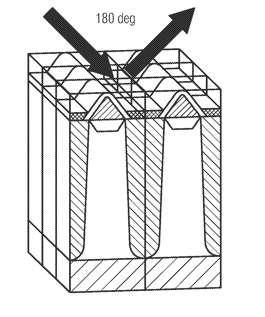
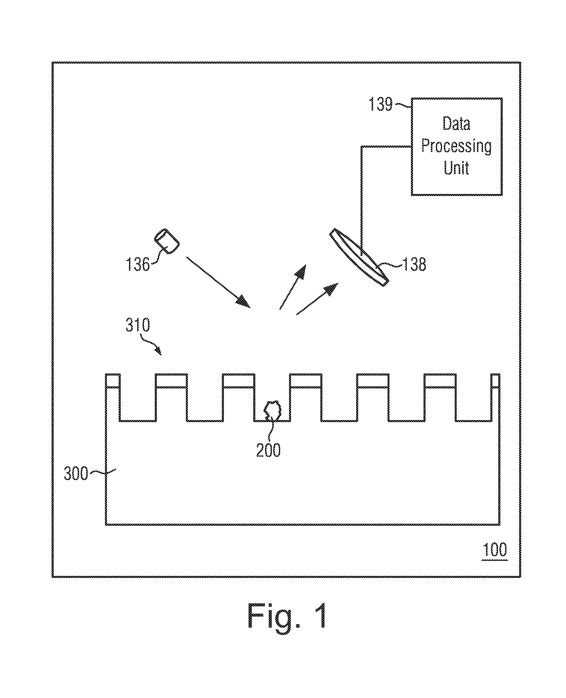
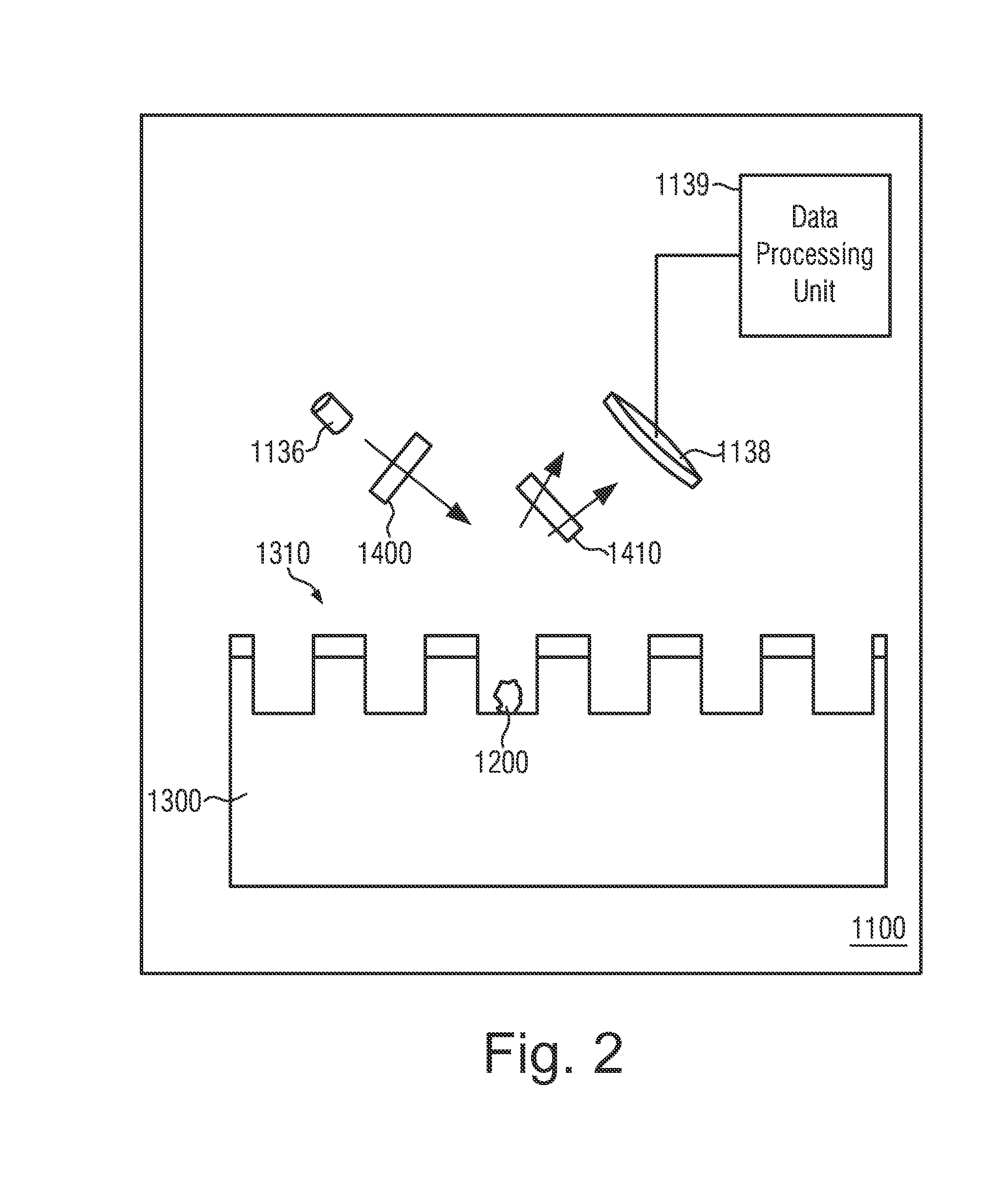
- An atypical use of scatterometry or ellipsometry tools for detecting particle contamination on semiconductor wafers by comparing measured metrology data with reference data, utilizing a metrology system with a light source, detector, and data processing unit to determine the presence of contaminants based on reflection profiles and polarization changes.

System and method for detecting particle contamination on a bonding tool
PatentPendingKR1020240036503A
Innovation
- A wafer shape metrology system that performs stress-free shape measurements on bonded wafer pairs, using a controller and machine learning algorithms to convert these measurements into overlay distortion patterns, enabling detection of localized deviations and contaminant particles on bonding devices.


Semiconductor Manufacturing Quality Standards and Compliance
Semiconductor manufacturing operates under stringent quality standards that directly impact contamination detection capabilities through wafer metrology techniques. The International Technology Roadmap for Semiconductors (ITRS) and its successor, the International Roadmap for Devices and Systems (IRDS), establish fundamental guidelines for contamination control requirements. These roadmaps specify maximum allowable particle densities, with current standards requiring detection of particles as small as 10-20 nanometers for advanced nodes below 7nm.
ISO 14644 standards govern cleanroom environments where wafer metrology operations occur, defining air cleanliness classifications that directly affect measurement accuracy. Class 1 cleanrooms, typically required for advanced semiconductor manufacturing, permit no more than 10 particles per cubic meter of 0.1 micrometers or larger. This environmental control is crucial for contamination pattern detection, as ambient particles can interfere with optical and electron beam metrology systems.
SEMI standards, particularly SEMI F47 for specification and guidelines for contamination monitoring equipment, establish protocols for wafer surface inspection and metrology tool qualification. These standards mandate specific detection sensitivity levels, measurement repeatability requirements, and calibration procedures that ensure consistent contamination pattern identification across different manufacturing facilities and equipment vendors.
Regulatory compliance frameworks such as IATF 16949 for automotive semiconductors and AS9100 for aerospace applications impose additional quality requirements that influence contamination detection methodologies. These sector-specific standards often require enhanced traceability and statistical process control measures, necessitating more sophisticated pattern recognition algorithms and data management systems within metrology tools.
The Semiconductor Equipment and Materials International (SEMI) M1 specification defines standard mechanical dimensions for silicon wafers, which directly impacts metrology tool design and contamination detection accuracy. Wafer flatness tolerances specified in SEMI M1 affect the precision of surface scanning techniques used in contamination pattern analysis.
Quality management systems compliant with ISO 9001 and semiconductor-specific extensions require documented procedures for contamination control and metrology validation. These compliance requirements drive the development of automated contamination classification systems and real-time monitoring capabilities that can provide audit trails and statistical evidence of process control effectiveness.
ISO 14644 standards govern cleanroom environments where wafer metrology operations occur, defining air cleanliness classifications that directly affect measurement accuracy. Class 1 cleanrooms, typically required for advanced semiconductor manufacturing, permit no more than 10 particles per cubic meter of 0.1 micrometers or larger. This environmental control is crucial for contamination pattern detection, as ambient particles can interfere with optical and electron beam metrology systems.
SEMI standards, particularly SEMI F47 for specification and guidelines for contamination monitoring equipment, establish protocols for wafer surface inspection and metrology tool qualification. These standards mandate specific detection sensitivity levels, measurement repeatability requirements, and calibration procedures that ensure consistent contamination pattern identification across different manufacturing facilities and equipment vendors.
Regulatory compliance frameworks such as IATF 16949 for automotive semiconductors and AS9100 for aerospace applications impose additional quality requirements that influence contamination detection methodologies. These sector-specific standards often require enhanced traceability and statistical process control measures, necessitating more sophisticated pattern recognition algorithms and data management systems within metrology tools.
The Semiconductor Equipment and Materials International (SEMI) M1 specification defines standard mechanical dimensions for silicon wafers, which directly impacts metrology tool design and contamination detection accuracy. Wafer flatness tolerances specified in SEMI M1 affect the precision of surface scanning techniques used in contamination pattern analysis.
Quality management systems compliant with ISO 9001 and semiconductor-specific extensions require documented procedures for contamination control and metrology validation. These compliance requirements drive the development of automated contamination classification systems and real-time monitoring capabilities that can provide audit trails and statistical evidence of process control effectiveness.
Cost-Benefit Analysis of Advanced Metrology Implementation
The implementation of advanced metrology systems for contamination pattern detection requires substantial capital investment, yet the financial returns can be significant when properly evaluated. Initial equipment costs for state-of-the-art metrology tools range from $2-8 million per system, depending on the technology complexity and measurement capabilities. These systems typically include scanning electron microscopes with enhanced detection algorithms, optical inspection tools with advanced pattern recognition, and specialized surface analysis equipment capable of detecting sub-nanometer contamination particles.
Operational expenses encompass maintenance contracts, consumables, and specialized personnel training, adding approximately 15-20% annually to the initial investment. However, these costs must be weighed against the substantial benefits of early contamination detection. Advanced metrology implementation can reduce yield losses by 3-8%, translating to millions of dollars in saved production costs for high-volume manufacturing facilities.
The return on investment becomes particularly compelling when considering the prevention of catastrophic contamination events. A single undetected contamination source can result in scrapping entire wafer lots, with losses potentially reaching $10-50 million depending on the production stage and wafer value. Advanced metrology systems provide early warning capabilities that can prevent such scenarios, offering risk mitigation worth several times the initial investment.
Time-to-detection improvements represent another significant benefit. Traditional contamination identification methods may require 24-72 hours, while advanced metrology can detect patterns within minutes to hours. This acceleration reduces the number of affected wafers and enables faster corrective actions, minimizing production disruptions and associated costs.
Long-term benefits include enhanced process control capabilities, improved customer satisfaction through higher quality products, and competitive advantages in advanced node manufacturing. The cumulative effect typically justifies the investment within 18-36 months for facilities processing high-value wafers, making advanced metrology implementation a strategically sound financial decision for semiconductor manufacturers focused on contamination pattern detection.
Operational expenses encompass maintenance contracts, consumables, and specialized personnel training, adding approximately 15-20% annually to the initial investment. However, these costs must be weighed against the substantial benefits of early contamination detection. Advanced metrology implementation can reduce yield losses by 3-8%, translating to millions of dollars in saved production costs for high-volume manufacturing facilities.
The return on investment becomes particularly compelling when considering the prevention of catastrophic contamination events. A single undetected contamination source can result in scrapping entire wafer lots, with losses potentially reaching $10-50 million depending on the production stage and wafer value. Advanced metrology systems provide early warning capabilities that can prevent such scenarios, offering risk mitigation worth several times the initial investment.
Time-to-detection improvements represent another significant benefit. Traditional contamination identification methods may require 24-72 hours, while advanced metrology can detect patterns within minutes to hours. This acceleration reduces the number of affected wafers and enables faster corrective actions, minimizing production disruptions and associated costs.
Long-term benefits include enhanced process control capabilities, improved customer satisfaction through higher quality products, and competitive advantages in advanced node manufacturing. The cumulative effect typically justifies the investment within 18-36 months for facilities processing high-value wafers, making advanced metrology implementation a strategically sound financial decision for semiconductor manufacturers focused on contamination pattern detection.
Unlock deeper insights with PatSnap Eureka Quick Research — get a full tech report to explore trends and direct your research. Try now!
Generate Your Research Report Instantly with AI Agent
Supercharge your innovation with PatSnap Eureka AI Agent Platform!