

How to Implement AI for Enhanced EUV Lithography Process Control
APR 2, 20269 MIN READ
Generate Your Research Report Instantly with AI Agent
Patsnap Eureka helps you evaluate technical feasibility & market potential.
AI-Enhanced EUV Lithography Background and Objectives
Extreme Ultraviolet (EUV) lithography represents a revolutionary advancement in semiconductor manufacturing, utilizing 13.5 nanometer wavelength light to achieve unprecedented pattern resolution for next-generation microprocessors and memory devices. This technology has emerged as the cornerstone for producing chips at 7nm, 5nm, and beyond, enabling the continuation of Moore's Law in an era where traditional optical lithography approaches physical limitations.
The evolution of EUV lithography spans over three decades of intensive research and development, beginning with initial concepts in the 1980s and reaching commercial viability in the 2010s. Key milestones include the development of high-power EUV light sources, advanced multilayer mirrors, and sophisticated resist materials capable of responding to EUV radiation. The technology's progression has been marked by significant challenges in source power scaling, mask defectivity control, and resist sensitivity optimization.
Current EUV systems operate in complex environments requiring precise control of numerous interdependent parameters including source power stability, optical alignment, thermal management, and contamination control. Traditional process control methods rely heavily on statistical process control and feedback mechanisms that often react to deviations after they occur, potentially resulting in yield losses and production inefficiencies.
The integration of artificial intelligence into EUV lithography process control aims to transform reactive control paradigms into predictive and adaptive systems. AI technologies, particularly machine learning algorithms and neural networks, offer unprecedented capabilities for pattern recognition, anomaly detection, and real-time optimization of complex multi-variable systems inherent in EUV manufacturing environments.
Primary objectives for AI-enhanced EUV process control include achieving real-time predictive maintenance capabilities, implementing advanced defect detection and classification systems, and establishing autonomous process optimization frameworks. These objectives target significant improvements in overall equipment effectiveness, reduction in unplanned downtime, and enhancement of yield performance through intelligent process parameter adjustment.
The strategic implementation of AI in EUV lithography seeks to address critical industry challenges including the need for higher throughput, improved yield stability, and reduced cost of ownership. By leveraging AI's capacity for continuous learning and adaptation, EUV systems can evolve beyond static control algorithms to become self-optimizing manufacturing platforms capable of responding dynamically to process variations and equipment drift patterns.
Market Demand for Advanced EUV Process Control Solutions
The semiconductor industry faces unprecedented challenges in maintaining yield and quality as EUV lithography becomes the cornerstone of advanced node manufacturing. With the transition to sub-7nm processes, traditional process control methods have reached their limitations, creating substantial market demand for AI-enhanced solutions that can handle the complexity and precision requirements of EUV systems.
Leading semiconductor manufacturers are experiencing significant yield losses due to the inherent complexities of EUV processes, including photon shot noise, mask defects, and thermal effects. These challenges translate directly into financial impact, as each percentage point of yield improvement can represent millions in revenue for high-volume production facilities. The industry's shift toward more sophisticated process control solutions reflects the critical need to maintain competitiveness in advanced manufacturing.
The market demand is particularly acute among foundries and memory manufacturers operating at the technology forefront. These companies require real-time process optimization capabilities that can adapt to the stochastic nature of EUV exposure and the minute variations in resist chemistry. Traditional rule-based control systems cannot adequately address the multidimensional parameter spaces involved in EUV processes, driving adoption of machine learning approaches.
Equipment manufacturers are responding to customer demands by integrating AI capabilities into their EUV systems. The market shows strong preference for solutions that can provide predictive maintenance, real-time dose optimization, and automated defect classification. These capabilities are essential for maximizing the substantial investments in EUV infrastructure, where system downtime costs can exceed hundreds of thousands per hour.
The growing complexity of multi-patterning schemes and the need for edge placement accuracy at atomic scales further amplify market demand. Customers seek integrated solutions that can correlate data across multiple process steps, enabling holistic optimization rather than isolated parameter adjustments. This systems-level approach represents a significant market opportunity for AI-driven process control platforms.
Emerging applications in advanced packaging and specialized devices are expanding the addressable market beyond traditional logic and memory segments. These applications often require customized process control strategies, creating demand for flexible AI frameworks that can be rapidly adapted to new process requirements and material systems.
Current EUV Lithography Challenges and AI Integration Status
Extreme Ultraviolet (EUV) lithography represents the cutting-edge technology for semiconductor manufacturing at advanced nodes below 7nm, yet it faces significant technical challenges that limit its widespread adoption and efficiency. The primary obstacles include source power limitations, photoresist sensitivity issues, mask defectivity, and stochastic effects that become increasingly problematic at smaller feature sizes.
Source power remains a critical bottleneck, with current EUV sources delivering approximately 250-300 watts of power, while industry targets exceed 500 watts for high-volume manufacturing. This limitation directly impacts throughput, making EUV lithography economically challenging for many applications. Additionally, the inherent instability of plasma-based EUV sources introduces dose variations that affect pattern fidelity and uniformity across wafers.
Photoresist materials present another significant challenge, as they must balance sensitivity, resolution, and line edge roughness. The stochastic nature of photon absorption at EUV wavelengths leads to shot noise effects, resulting in critical dimension uniformity issues and increased defectivity rates. These phenomena become more pronounced as feature sizes approach the molecular scale of resist materials.
Mask defectivity poses substantial concerns due to the reflective nature of EUV masks and the extreme sensitivity to particle contamination. Even sub-nanometer particles can cause printable defects, requiring unprecedented cleanliness levels throughout the lithography process. The multilayer mirror structure of EUV masks also introduces phase and amplitude variations that affect imaging performance.
Current AI integration in EUV lithography remains in early stages, primarily focused on predictive maintenance and basic process optimization. Machine learning algorithms are being deployed for source power prediction, enabling proactive adjustments to maintain stable exposure conditions. Pattern recognition systems assist in defect classification and root cause analysis, though their implementation is limited to specific process steps.
Advanced process control systems are beginning to incorporate neural networks for real-time dose correction and overlay optimization. These systems analyze historical process data to predict optimal exposure parameters, reducing the need for extensive test wafer runs. However, the integration remains fragmented, with AI solutions addressing individual process challenges rather than providing comprehensive system-level optimization.
The semiconductor industry recognizes AI's potential to address EUV's fundamental challenges through intelligent process control, predictive modeling, and automated decision-making. Current research focuses on developing AI frameworks capable of handling the complex, multi-variable nature of EUV processes while ensuring the reliability and precision required for advanced semiconductor manufacturing.
Existing AI-Based Process Control Solutions for EUV
01 Machine learning for defect detection and classification in EUV lithography
Artificial intelligence and machine learning algorithms can be applied to analyze images and data from EUV lithography processes to detect, identify, and classify defects. These AI-based systems can process large amounts of inspection data to recognize patterns and anomalies that may indicate process variations or defects. By training neural networks on historical defect data, the system can automatically categorize defects and provide feedback for process optimization, improving yield and reducing manual inspection time.- Machine learning for defect detection and classification in EUV lithography: Artificial intelligence and machine learning algorithms can be applied to analyze images and data from EUV lithography processes to detect, identify, and classify defects. These AI-based systems can learn patterns from historical data to improve defect recognition accuracy, enabling real-time quality control and reducing false positives. The machine learning models can be trained on various defect types and process variations to enhance the robustness of defect detection systems.
- AI-driven process parameter optimization and control: Artificial intelligence systems can be utilized to optimize and control critical process parameters in EUV lithography by analyzing multiple input variables and their correlations. These systems can predict optimal parameter settings based on desired output characteristics and automatically adjust process conditions in real-time. The AI algorithms can learn from process feedback to continuously improve parameter control strategies and maintain process stability across different operating conditions.
- Predictive maintenance and equipment health monitoring using AI: AI-based predictive maintenance systems can monitor equipment health and predict potential failures in EUV lithography tools by analyzing sensor data and operational parameters. These systems can identify anomalies and degradation patterns before they lead to equipment downtime or process deviations. Machine learning models can be trained to recognize early warning signs of component wear or malfunction, enabling proactive maintenance scheduling and reducing unplanned downtime.
- Neural network-based overlay and alignment control: Neural networks and deep learning techniques can be employed to improve overlay accuracy and alignment control in EUV lithography processes. These AI systems can process complex metrology data to predict and compensate for overlay errors caused by various process factors. The neural network models can learn non-linear relationships between process conditions and overlay performance, enabling more precise control than traditional methods.
- AI-enhanced dose control and exposure optimization: Artificial intelligence algorithms can optimize dose control and exposure settings in EUV lithography by analyzing the relationship between exposure parameters and pattern fidelity. These systems can predict the required dose adjustments for different pattern densities and feature types to achieve uniform critical dimension control. AI models can incorporate feedback from metrology measurements to continuously refine dose control strategies and compensate for process variations.
02 AI-driven overlay and alignment control
Advanced process control systems utilize artificial intelligence to optimize overlay accuracy and alignment in EUV lithography. These systems employ predictive models and real-time data analysis to compensate for systematic errors and drift in the lithography process. By continuously monitoring alignment marks and overlay measurements, AI algorithms can adjust exposure parameters and stage positioning to maintain tight overlay specifications across the wafer, which is critical for advanced node manufacturing.Expand Specific Solutions03 Predictive maintenance and equipment health monitoring using AI
Artificial intelligence systems can monitor the health and performance of EUV lithography equipment by analyzing sensor data, operational parameters, and historical maintenance records. These predictive maintenance solutions use machine learning models to identify early warning signs of equipment degradation or potential failures before they impact production. By forecasting maintenance needs and optimizing service schedules, AI-driven systems help maximize equipment uptime and extend the operational life of expensive EUV tools.Expand Specific Solutions04 AI-based dose and focus optimization
Process control systems employ artificial intelligence to optimize exposure dose and focus settings in EUV lithography. These systems analyze metrology data from test patterns and production wafers to determine optimal process windows. Machine learning algorithms can model the complex relationships between process parameters and lithographic outcomes, enabling automatic adjustment of dose and focus to compensate for variations in resist properties, substrate topography, and environmental conditions, thereby improving critical dimension uniformity and process stability.Expand Specific Solutions05 Neural network-based optical proximity correction and process modeling
Artificial intelligence techniques, particularly deep learning and neural networks, can be applied to enhance optical proximity correction and process modeling for EUV lithography. These AI-based approaches can learn complex relationships between mask patterns and printed wafer results, enabling more accurate prediction of lithographic outcomes. By training on extensive simulation and empirical data, neural networks can generate optimized mask designs and provide fast, accurate process models that account for various physical effects in EUV lithography, reducing the time required for mask design iterations and improving pattern fidelity.Expand Specific Solutions
Key Players in EUV Equipment and AI Technology
The EUV lithography AI implementation landscape represents a mature, high-stakes market dominated by established semiconductor giants and specialized equipment manufacturers. The industry is in an advanced consolidation phase with substantial market size driven by critical 7nm and below node requirements. Technology maturity varies significantly across players: ASML Netherlands BV leads with cutting-edge EUV systems, while Taiwan Semiconductor Manufacturing Co. and Samsung Electronics demonstrate advanced AI integration capabilities in production environments. Equipment specialists like Applied Materials, Lam Research Corp., and KLA Corp. are rapidly developing AI-enhanced process control solutions. Chinese players including SMIC and Shanghai Sinyang are aggressively pursuing technological catch-up through substantial R&D investments. The competitive dynamics reflect a two-tier structure where leading foundries and equipment manufacturers possess mature AI implementations, while emerging players focus on specialized applications and cost-effective solutions to capture market share.
Taiwan Semiconductor Manufacturing Co., Ltd.
Technical Solution: TSMC has developed a comprehensive AI-powered EUV process control framework that combines machine learning with advanced process monitoring systems. Their approach utilizes convolutional neural networks for real-time defect detection and classification during EUV exposure, achieving defect detection rates exceeding 95% accuracy. The system incorporates predictive maintenance algorithms that analyze equipment sensor data to forecast potential issues before they impact production yield. TSMC's AI solution also includes automated recipe optimization that continuously learns from production data to refine exposure parameters, resulting in improved critical dimension uniformity and reduced cycle times. Their implementation has demonstrated yield improvements of 15-25% in advanced node production while reducing overall process variability.
Strengths: Extensive manufacturing experience with proven AI implementation at scale and strong yield optimization results. Weaknesses: Proprietary solutions may have limited transferability to other manufacturing environments.
Lam Research Corp.
Technical Solution: Lam Research has developed AI-enhanced process control solutions for EUV lithography through their Sense.i platform, which combines advanced sensors with machine learning algorithms for real-time process optimization. Their system utilizes artificial intelligence to analyze plasma and etch process data in conjunction with EUV lithography parameters to optimize overall patterning performance. The AI framework employs predictive modeling to anticipate process variations and automatically adjust downstream processing steps to compensate for EUV-induced variations. Lam's solution includes intelligent recipe management that learns from historical data to continuously improve process outcomes and reduce variability. The platform also features automated anomaly detection that can identify subtle process deviations that might impact final device performance, enabling proactive process control and yield optimization.
Strengths: Strong expertise in plasma processing with innovative AI integration and comprehensive process optimization capabilities. Weaknesses: Focus primarily on etch processes may limit comprehensive EUV lithography control coverage.
Core AI Algorithms for EUV Process Optimization
EUV Lithography System With 3D Sensing and Tunning Modules
PatentActiveUS20240103378A1
Innovation
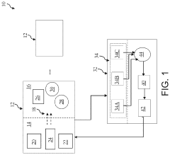
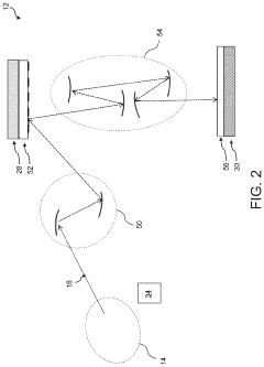
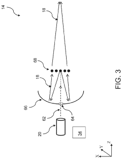
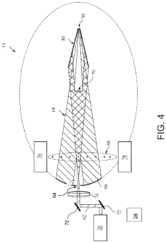
- An EUV lithography system integrated with a 3D diagnostic module and control system that monitors and analyzes laser beam, plasma, and EUV radiation parameters, using correlation analysis, machine learning, and real-time tuning to optimize the lithography process, reducing debris and enhancing EUV radiation energy.
Mixed energy control in an EUV lithography system
PatentWO2024056330A1
Innovation
- A mixed energy control system employing two cooperative control loops: one for controlling the RF excitation signal's energy and another for managing hit/miss firing patterns, which adjusts the energy of individual EUV pulses and determines which droplets are irradiated, using a plasma sensor to maintain stability and avoid detrimental firing patterns.


Semiconductor Industry Standards and AI Compliance
The integration of AI technologies into EUV lithography process control must navigate a complex landscape of semiconductor industry standards and regulatory compliance requirements. The semiconductor industry operates under stringent quality and safety standards, including ISO 9001 for quality management systems, ISO 14001 for environmental management, and SEMI standards specifically designed for semiconductor manufacturing equipment and processes.
AI implementation in EUV lithography systems must comply with SEMI E10 standard for equipment safety guidelines and SEMI E30 for generic model for communications and control of manufacturing equipment. These standards ensure that AI-enhanced control systems maintain the reliability and safety protocols essential for semiconductor manufacturing environments. Additionally, compliance with SEMI E125 standard for specification for equipment self-description is crucial when implementing AI diagnostic and predictive maintenance capabilities.
Data governance and cybersecurity compliance present significant challenges for AI-enabled EUV systems. The semiconductor industry increasingly adheres to frameworks such as NIST Cybersecurity Framework and ISO 27001 for information security management. AI systems processing sensitive manufacturing data must implement robust encryption, access controls, and audit trails to meet these requirements while maintaining real-time processing capabilities.
Regulatory compliance extends to international trade regulations, particularly regarding dual-use technology restrictions. AI algorithms embedded in EUV lithography equipment may be subject to export control regulations under frameworks such as the Wassenaar Arrangement and national export administration regulations. This necessitates careful consideration of AI model architecture and data handling to ensure compliance across different jurisdictions.
Quality assurance standards specific to AI implementation are emerging within the semiconductor industry. The development of AI models for process control must follow validation protocols that demonstrate repeatability, traceability, and statistical process control compliance. This includes establishing clear metrics for AI model performance, implementing version control systems, and maintaining comprehensive documentation for regulatory audits.
The industry is also developing specific guidelines for AI transparency and explainability in critical manufacturing processes. These emerging standards require AI systems to provide interpretable decision-making processes, particularly when controlling critical parameters in EUV lithography that directly impact yield and product quality.
Data Security and IP Protection in AI-EUV Systems
The integration of artificial intelligence into extreme ultraviolet lithography systems introduces unprecedented data security challenges that require comprehensive protection frameworks. EUV lithography processes generate massive volumes of sensitive manufacturing data, including proprietary process parameters, defect patterns, and yield optimization algorithms. This data represents critical intellectual property that must be safeguarded against unauthorized access, industrial espionage, and potential cyber threats.
AI-enhanced EUV systems create multiple attack vectors that traditional semiconductor security measures may not adequately address. Machine learning models themselves become valuable intellectual property, containing embedded knowledge about optimal process conditions, predictive algorithms, and proprietary optimization techniques. The real-time nature of AI-driven process control requires continuous data exchange between sensors, control systems, and cloud-based analytics platforms, expanding the potential security perimeter significantly.
Data encryption protocols must be implemented at multiple levels within AI-EUV architectures. Edge computing devices collecting sensor data require hardware-based encryption capabilities to protect information during transmission and storage. Advanced encryption standards should be applied to both data-at-rest and data-in-transit scenarios, with particular attention to protecting training datasets and model parameters that could reveal competitive advantages if compromised.
Access control mechanisms must incorporate role-based permissions and multi-factor authentication systems specifically designed for manufacturing environments. Biometric authentication, secure token systems, and time-limited access credentials help ensure that only authorized personnel can interact with critical AI algorithms and process control systems. Network segmentation strategies should isolate AI-EUV systems from broader corporate networks while maintaining necessary connectivity for remote monitoring and support functions.
Intellectual property protection extends beyond traditional data security to encompass AI model protection techniques. Federated learning approaches can enable collaborative development while maintaining data privacy, allowing multiple facilities to benefit from shared AI improvements without exposing proprietary process information. Model watermarking and fingerprinting technologies help detect unauthorized copying or reverse engineering of AI algorithms, providing legal recourse against IP theft.
Regular security audits and penetration testing specifically tailored for AI-enhanced manufacturing systems become essential components of comprehensive protection strategies, ensuring that evolving cyber threats are identified and mitigated before they can compromise critical lithography operations.
Unlock deeper insights with Patsnap Eureka Quick Research — get a full tech report to explore trends and direct your research. Try now!
Generate Your Research Report Instantly with AI Agent
Supercharge your innovation with Patsnap Eureka AI Agent Platform!