How to Implement Machine Learning in EUV Lithography Optimization
APR 2, 20269 MIN READ
Generate Your Research Report Instantly with AI Agent
Patsnap Eureka helps you evaluate technical feasibility & market potential.
EUV Lithography ML Integration Background and Objectives
Extreme Ultraviolet (EUV) lithography represents a critical technological breakthrough in semiconductor manufacturing, enabling the production of advanced microprocessors and memory devices with feature sizes below 7 nanometers. As the semiconductor industry continues to push the boundaries of Moore's Law, EUV lithography has emerged as the primary solution for achieving the precision and resolution required for next-generation integrated circuits. However, the complexity of EUV processes presents unprecedented challenges in process optimization, yield enhancement, and defect mitigation.
The evolution of EUV lithography technology spans over two decades of intensive research and development. Initial conceptualization began in the 1990s, with significant milestones achieved through collaborative efforts between semiconductor manufacturers, equipment suppliers, and research institutions. The technology transitioned from laboratory demonstrations to pilot production in the 2010s, culminating in high-volume manufacturing adoption by leading foundries around 2018-2019.
Traditional optimization approaches in EUV lithography rely heavily on physics-based models and empirical methods, which often prove insufficient for handling the multidimensional parameter spaces and complex interdependencies inherent in EUV processes. The stochastic nature of EUV photon interactions, mask defect compensation, and source-mask optimization present computational challenges that exceed the capabilities of conventional optimization techniques.
Machine learning integration into EUV lithography optimization aims to address these limitations by leveraging advanced algorithms capable of processing vast datasets, identifying non-linear relationships, and providing predictive insights for process control. The primary objectives include enhancing critical dimension uniformity, reducing line edge roughness, minimizing defect density, and optimizing throughput while maintaining stringent quality standards.
The strategic implementation of machine learning in EUV lithography seeks to establish adaptive process control systems that can respond dynamically to process variations, predict potential failure modes, and optimize multiple parameters simultaneously. This integration represents a paradigm shift from reactive to predictive manufacturing, enabling proactive adjustments that improve yield and reduce production costs while accelerating time-to-market for advanced semiconductor devices.
Market Demand for AI-Enhanced EUV Manufacturing
The semiconductor industry is experiencing unprecedented demand for advanced manufacturing capabilities, with extreme ultraviolet lithography representing the cornerstone technology for producing next-generation microprocessors and memory devices. As device geometries continue to shrink below 7nm nodes, traditional lithography optimization methods have reached their practical limits, creating substantial market pressure for innovative solutions that can enhance manufacturing precision and yield rates.
Global semiconductor manufacturers are increasingly recognizing that artificial intelligence integration into EUV processes represents a critical competitive advantage. The complexity of EUV lithography systems, involving intricate interactions between photon sources, optical systems, photoresists, and substrate materials, generates vast amounts of process data that traditional analytical methods cannot effectively utilize. This data richness presents significant opportunities for machine learning applications to unlock previously inaccessible optimization potential.
Market drivers for AI-enhanced EUV manufacturing stem from multiple industry pressures. Fabrication facilities face mounting costs associated with EUV equipment operation, including mask complexity, source power requirements, and throughput limitations. Manufacturing yields directly impact profitability, making process optimization technologies highly valuable investments. Additionally, the increasing sophistication of semiconductor designs demands more precise pattern fidelity and reduced variability across wafer surfaces.
Leading foundries and integrated device manufacturers are actively seeking solutions that can predict and compensate for process variations in real-time. The ability to dynamically adjust exposure parameters, optimize dose distributions, and predict defect formation patterns represents substantial value propositions. These capabilities can significantly reduce development cycles for new process nodes while improving manufacturing consistency and reducing waste.
The market opportunity extends beyond traditional semiconductor applications into emerging sectors requiring advanced lithography capabilities. High-performance computing, artificial intelligence accelerators, and quantum computing devices all demand the precision manufacturing that AI-enhanced EUV systems can provide. This expanding application base creates sustained demand for intelligent manufacturing solutions.
Investment patterns indicate strong industry commitment to developing AI-integrated lithography platforms. Equipment manufacturers, software developers, and semiconductor producers are forming strategic partnerships to accelerate technology development and deployment. The convergence of machine learning expertise with deep lithography knowledge represents a key market differentiator for companies positioning themselves in this evolving landscape.
Current EUV Process Challenges and ML Implementation Gaps
EUV lithography faces significant process challenges that create substantial barriers for effective machine learning implementation. Stochastic effects represent one of the most critical issues, where photon shot noise leads to random variations in pattern formation at the nanoscale. These variations manifest as line edge roughness, contact hole size variations, and defect formation, creating unpredictable process outcomes that are difficult to model using traditional deterministic approaches.
Mask defects pose another major challenge, as even nanometer-scale imperfections on EUV masks can cause significant pattern distortions on wafers. The complex interaction between mask defects, optical proximity effects, and resist chemistry creates a multidimensional problem space that requires sophisticated modeling approaches. Current defect compensation methods rely heavily on empirical corrections rather than predictive models.
Resist chemistry optimization remains a bottleneck in EUV processing. The trade-off between resolution, line edge roughness, and sensitivity creates a complex optimization landscape where traditional design of experiments approaches prove insufficient. The chemical amplification process in EUV resists involves numerous reaction pathways that are sensitive to environmental conditions and exposure parameters.
Machine learning implementation faces several critical gaps in the EUV domain. Data quality and availability represent primary obstacles, as EUV processes generate massive amounts of heterogeneous data from various metrology tools, but this data often lacks proper labeling and standardization. The high dimensionality of process parameters combined with limited training datasets creates challenges for model generalization.
Real-time processing requirements create additional implementation barriers. EUV lithography systems operate with throughput constraints that demand millisecond-level decision making for process adjustments. Current ML models often require computational resources that exceed the timing budgets available in production environments.
Integration complexity emerges from the need to interface ML algorithms with existing process control systems. Legacy equipment architectures were not designed for AI integration, creating compatibility issues and requiring significant infrastructure modifications. The lack of standardized data formats across different tool vendors further complicates seamless ML deployment.
Model interpretability represents a crucial gap in EUV ML applications. The semiconductor industry requires explainable AI solutions for process control decisions, but many effective ML algorithms operate as black boxes. This creates regulatory and quality assurance challenges that must be addressed before widespread adoption can occur.
Existing ML Algorithms for EUV Process Optimization
01 Hyperparameter tuning and model selection optimization
Methods and systems for automatically optimizing hyperparameters in machine learning models to improve performance. This includes techniques for efficient search strategies, automated parameter selection, and adaptive tuning mechanisms that reduce computational costs while maximizing model accuracy. The optimization process can involve grid search, random search, Bayesian optimization, or evolutionary algorithms to identify optimal configurations.- Hyperparameter tuning and model selection optimization: Machine learning optimization can be achieved through automated hyperparameter tuning techniques that systematically search for optimal model configurations. This includes methods such as grid search, random search, and Bayesian optimization to identify the best combination of parameters that maximize model performance. Advanced techniques employ meta-learning approaches to transfer knowledge across different optimization tasks and reduce computational costs.
- Neural architecture search and automated model design: Optimization techniques focus on automatically discovering optimal neural network architectures through systematic search methods. This involves using evolutionary algorithms, reinforcement learning, or gradient-based methods to explore the architecture space and identify efficient model structures. The approach reduces manual design effort while improving model accuracy and computational efficiency for specific tasks.
- Training efficiency and convergence acceleration: Methods for optimizing the training process include advanced gradient descent variants, adaptive learning rate scheduling, and distributed training strategies. These techniques aim to reduce training time, improve convergence stability, and enable efficient utilization of computational resources. Approaches may incorporate momentum-based methods, second-order optimization, and batch normalization strategies to enhance learning dynamics.
- Resource-constrained optimization and model compression: Optimization strategies for deploying machine learning models on resource-limited devices include pruning, quantization, and knowledge distillation techniques. These methods reduce model size and computational requirements while maintaining acceptable performance levels. The optimization process balances trade-offs between model accuracy, inference speed, memory footprint, and energy consumption for edge computing applications.
- Multi-objective and constrained optimization frameworks: Advanced optimization frameworks address multiple competing objectives simultaneously, such as accuracy, latency, and fairness constraints. These methods employ Pareto optimization, constraint satisfaction techniques, and regularization strategies to find optimal solutions that satisfy various requirements. The frameworks enable practitioners to balance different performance metrics and operational constraints in real-world deployment scenarios.
02 Training efficiency and computational resource optimization
Techniques for reducing training time and computational resource consumption in machine learning systems. This includes distributed training methods, gradient optimization algorithms, memory management strategies, and hardware acceleration approaches. The methods enable faster convergence, reduced energy consumption, and efficient utilization of processing units during model training phases.Expand Specific Solutions03 Neural network architecture optimization
Systems and methods for automatically designing and optimizing neural network architectures. This encompasses neural architecture search techniques, pruning methods, quantization strategies, and structural optimization approaches that balance model complexity with performance requirements. The optimization can adapt network topology, layer configurations, and connection patterns to achieve better accuracy with fewer parameters.Expand Specific Solutions04 Feature selection and dimensionality reduction optimization
Methods for optimizing input feature sets and reducing data dimensionality in machine learning pipelines. This includes automated feature engineering, relevance scoring, redundancy elimination, and transformation techniques that improve model performance while reducing computational complexity. The approaches help identify the most informative features and eliminate noise from training data.Expand Specific Solutions05 Inference optimization and deployment efficiency
Techniques for optimizing machine learning model inference in production environments. This includes model compression, runtime optimization, batch processing strategies, and edge deployment methods that reduce latency and improve throughput. The optimization focuses on making trained models more efficient for real-time predictions while maintaining accuracy in deployed applications.Expand Specific Solutions
Key Players in EUV Equipment and ML Software Solutions
The EUV lithography optimization market represents a mature yet rapidly evolving industry segment driven by the semiconductor industry's transition to advanced process nodes below 7nm. The market demonstrates substantial growth potential, with global EUV equipment investments exceeding $20 billion annually as foundries and memory manufacturers accelerate adoption. Technology maturity varies significantly across the competitive landscape, with ASML Netherlands maintaining dominant market position in EUV scanner systems, while companies like Taiwan Semiconductor Manufacturing Co., Samsung Electronics, and Intel lead in process optimization and implementation. Equipment suppliers including Lam Research, KLA Corp., and Carl Zeiss SMT provide critical subsystems and metrology solutions. Chinese players such as Semiconductor Manufacturing International and SMIC-Beijing are rapidly developing capabilities, while research institutions like Beijing Institute of Technology and Xiamen University contribute fundamental research. The integration of machine learning represents an emerging frontier, with established players leveraging AI for yield optimization, defect prediction, and process control enhancement.
Taiwan Semiconductor Manufacturing Co., Ltd.
Technical Solution: TSMC employs machine learning extensively in their EUV lithography optimization through advanced process control (APC) systems and predictive analytics. Their ML implementation focuses on hotspot detection, optical proximity correction (OPC), and source mask optimization (SMO). TSMC uses convolutional neural networks to identify potential lithographic hotspots before manufacturing, reducing the need for extensive simulations. Their machine learning algorithms analyze historical process data to predict optimal exposure conditions, including dose and focus settings. The company also implements reinforcement learning for dynamic process adjustments and uses ML-driven virtual metrology to predict wafer quality without physical measurements.
Strengths: Extensive manufacturing data for ML model training, leading-edge process expertise, strong R&D capabilities. Weaknesses: Complex integration with existing manufacturing systems, requires continuous model updates as processes evolve.
Samsung Electronics Co., Ltd.
Technical Solution: Samsung implements machine learning in EUV lithography through intelligent process monitoring and predictive maintenance systems. Their approach includes ML-based dose optimization algorithms that learn from wafer-to-wafer variations to minimize critical dimension uniformity issues. Samsung uses deep learning models for real-time defect classification and root cause analysis during EUV exposure processes. Their machine learning framework incorporates computer vision techniques for automated pattern recognition and overlay measurement optimization. The company also employs ML algorithms for predictive equipment maintenance, analyzing sensor data to prevent EUV scanner downtime and optimize tool performance across their fabrication facilities.
Strengths: Strong semiconductor manufacturing expertise, advanced data analytics capabilities, integrated approach across memory and logic production. Weaknesses: Relatively newer to leading-edge EUV processes compared to TSMC, requires significant investment in ML infrastructure.
Core ML Patents and Innovations in EUV Lithography
Source mask optimization by process defects prediction
PatentActiveUS20210264091A1
Innovation
- The implementation of defect-aware simulation models and optimization techniques that incorporate stochastic variables to predict defect rates and optimize source illumination and mask design, using modules for process simulation, optical proximity correction, and cost function optimization to enhance wafer yield and reduce production costs.


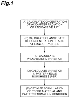
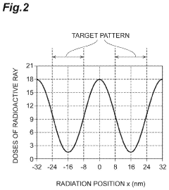
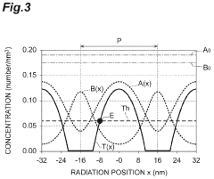
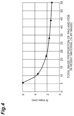
Method of simulating resist pattern, resist material and method of optimizing formulation thereof, apparatus and recording medium
PatentActiveUS20200057371A1
Innovation
- A simulation method and resist material formulation optimization that accounts for probabilistic variations in photon noise and active species distribution, using a chemical amplification-type resist material with a photo-acid-generating agent and photodecomposable quencher, to minimize pattern edge roughness and sensitivity variations.
Semiconductor Industry Standards for ML Integration
The semiconductor industry has established several foundational standards that facilitate the integration of machine learning technologies into manufacturing processes, particularly for EUV lithography optimization. The International Semiconductor Equipment and Materials International (SEMI) organization has developed comprehensive guidelines under the SEMI E187 standard, which specifically addresses the implementation of artificial intelligence and machine learning in semiconductor manufacturing environments. This standard provides a framework for data collection, model validation, and performance metrics essential for ML deployment in critical manufacturing processes.
Industry-wide adoption of the Manufacturing Execution System (MES) standards, particularly SEMI E90 and E94, creates a standardized data infrastructure that enables seamless ML integration. These standards ensure consistent data formats, real-time data streaming capabilities, and interoperability between different equipment vendors' systems. For EUV lithography applications, this standardization is crucial as it allows ML algorithms to access and process data from multiple sources including scanner telemetry, metrology tools, and process control systems in a unified manner.
The Semiconductor Equipment Communications Standard (SECS/GEM) protocols, specifically SEMI E4, E5, and E30, provide the communication backbone necessary for ML systems to interface with EUV lithography equipment. These standards define message structures, data collection events, and equipment control mechanisms that ML algorithms require for real-time optimization. The standardized communication protocols ensure that ML models can receive consistent, high-quality data streams and execute control decisions across different equipment platforms.
Quality management standards such as ISO 9001 and automotive-specific IATF 16949 have been adapted for ML integration, establishing requirements for model lifecycle management, validation procedures, and traceability. These standards mandate rigorous documentation of ML model development, training data provenance, and performance monitoring, which are essential for maintaining the reliability and repeatability required in semiconductor manufacturing.
The emerging IEEE 2857 standard for privacy engineering and the ISO/IEC 23053 framework for AI risk management provide additional governance structures for ML implementation. These standards address critical concerns regarding intellectual property protection, data security, and algorithmic transparency that are paramount when deploying ML solutions in competitive semiconductor manufacturing environments, ensuring that EUV lithography optimization benefits from ML capabilities while maintaining operational security and compliance requirements.
Data Security and IP Protection in EUV ML Systems
The integration of machine learning systems into EUV lithography processes introduces significant data security and intellectual property protection challenges that require comprehensive safeguarding strategies. EUV manufacturing environments generate vast amounts of proprietary data, including process parameters, defect patterns, and optimization algorithms that represent substantial competitive advantages and trade secrets.
Data encryption protocols form the foundation of security architecture in EUV ML systems. Advanced encryption standards must be implemented across all data transmission channels, storage systems, and processing nodes. Multi-layered encryption approaches, including end-to-end encryption for data in transit and robust encryption for data at rest, ensure that sensitive lithography parameters and machine learning models remain protected from unauthorized access.
Access control mechanisms require sophisticated implementation to balance operational efficiency with security requirements. Role-based access control systems must be established to restrict data access based on personnel clearance levels and operational necessity. Biometric authentication, multi-factor authentication, and time-limited access tokens provide additional security layers for accessing critical ML training datasets and proprietary algorithms.
Intellectual property protection extends beyond traditional data security to encompass machine learning model protection. Model watermarking techniques and adversarial training methods help prevent unauthorized model extraction and reverse engineering. Federated learning approaches enable collaborative model development while maintaining data locality and reducing exposure risks of sensitive manufacturing data.
Secure computing environments, including hardware security modules and trusted execution environments, provide isolated processing capabilities for sensitive ML computations. These environments ensure that proprietary algorithms and training processes remain protected even during active computation phases, preventing potential data leakage through side-channel attacks or unauthorized system access.
Compliance frameworks must address both industry-specific regulations and international data protection standards. Regular security audits, penetration testing, and vulnerability assessments ensure ongoing protection effectiveness while maintaining operational continuity in high-volume manufacturing environments.
Unlock deeper insights with Patsnap Eureka Quick Research — get a full tech report to explore trends and direct your research. Try now!
Generate Your Research Report Instantly with AI Agent
Supercharge your innovation with Patsnap Eureka AI Agent Platform!