How To Improve Photolithography Through Diffraction Reduction Techniques
FEB 24, 20269 MIN READ
Generate Your Research Report Instantly with AI Agent
Patsnap Eureka helps you evaluate technical feasibility & market potential.
Photolithography Diffraction Reduction Background and Objectives
Photolithography stands as the cornerstone technology enabling the semiconductor industry's relentless pursuit of Moore's Law, facilitating the fabrication of increasingly complex integrated circuits with ever-shrinking feature sizes. Since its inception in the 1960s, this optical patterning technique has evolved from producing micrometer-scale features to achieving sub-10-nanometer resolution in contemporary manufacturing processes. However, as the industry pushes toward nodes below 7nm and approaches the 3nm frontier, fundamental physical limitations imposed by optical diffraction have emerged as critical barriers to further advancement.
The phenomenon of diffraction, an inherent property of electromagnetic wave propagation, causes light to spread and interfere when passing through narrow apertures or around pattern edges. This effect becomes increasingly problematic as feature dimensions approach and fall below the wavelength of the exposure light source. In modern deep ultraviolet (DUV) lithography systems operating at 193nm wavelength, and even in extreme ultraviolet (EUV) systems at 13.5nm, diffraction-induced pattern distortion, edge blurring, and resolution degradation directly impact manufacturing yield and device performance.
The primary objective of diffraction reduction research is to develop comprehensive technical solutions that enable photolithography systems to reliably pattern features significantly smaller than the exposure wavelength while maintaining acceptable process windows and manufacturing economics. This encompasses multiple strategic goals: enhancing optical resolution limits through advanced illumination schemes, developing sophisticated computational lithography techniques for pattern optimization, implementing novel photoresist materials with improved response characteristics, and exploring hybrid approaches that combine multiple diffraction mitigation strategies.
Secondary objectives include reducing manufacturing complexity and cost associated with multiple patterning techniques currently required for advanced nodes, improving pattern fidelity and edge placement accuracy to meet stringent design requirements, and establishing scalable solutions that can support future technology nodes beyond current roadmap projections. These efforts aim to extend the viability of optical lithography while bridging toward next-generation patterning technologies, ensuring continued semiconductor industry advancement and enabling emerging applications in artificial intelligence, quantum computing, and advanced communications infrastructure.
Market Demand for Advanced Lithography Solutions
The semiconductor industry's relentless pursuit of smaller, faster, and more energy-efficient chips has positioned advanced photolithography as a critical enabler of next-generation electronics. As device geometries shrink below the 7-nanometer node and approach the 3-nanometer and 2-nanometer thresholds, traditional lithography techniques face fundamental physical limitations imposed by optical diffraction. This challenge has created substantial market demand for innovative diffraction reduction solutions that can extend the capabilities of existing lithography platforms while maintaining economic viability.
The proliferation of artificial intelligence, high-performance computing, 5G infrastructure, and Internet of Things applications has intensified the need for advanced semiconductor manufacturing capabilities. Data centers require processors with higher transistor densities to handle increasingly complex computational workloads, while mobile devices demand chips that balance performance with power efficiency. These application-driven requirements translate directly into demand for lithography systems capable of producing finer features with greater precision and throughput.
Major semiconductor manufacturers are investing heavily in next-generation fabrication facilities equipped with advanced lithography tools. The transition from deep ultraviolet lithography to extreme ultraviolet systems represents a significant capital commitment, yet even these cutting-edge platforms benefit from complementary diffraction reduction techniques such as computational lithography, advanced photoresists, and multi-patterning strategies. The market demonstrates strong appetite for hybrid solutions that combine multiple diffraction mitigation approaches to achieve target resolutions.
Geographic concentration of semiconductor manufacturing in specific regions has created localized demand hotspots for advanced lithography solutions. Foundries and integrated device manufacturers in these regions compete intensely for technological leadership, driving continuous investment in process innovation. Supply chain considerations and geopolitical factors further amplify demand as nations seek to establish domestic semiconductor manufacturing capabilities with state-of-the-art lithography infrastructure.
The economic value proposition of diffraction reduction techniques extends beyond pure resolution enhancement. Improved process windows, reduced defect densities, and enhanced yield stability represent tangible benefits that justify technology adoption. As manufacturing costs escalate with each process node, solutions that improve first-pass yield or extend equipment lifetimes generate substantial return on investment, reinforcing market demand for proven diffraction management technologies.
Current Diffraction Challenges in Photolithography Systems
Diffraction remains one of the most fundamental physical limitations constraining the advancement of photolithography systems toward smaller feature sizes. As semiconductor manufacturing pushes toward sub-3nm technology nodes, the wavelength-dependent nature of light diffraction creates increasingly severe challenges that directly impact resolution, pattern fidelity, and manufacturing yield. Current deep ultraviolet lithography systems operating at 193nm wavelengths face inherent diffraction limits that blur the boundaries of projected patterns, particularly when feature dimensions approach or fall below the exposure wavelength.
The primary challenge manifests in the form of optical proximity effects, where diffraction causes adjacent features to interact unpredictably, leading to pattern distortions, corner rounding, and line-end shortening. These effects become exponentially more pronounced as the numerical aperture of optical systems increases and as target feature sizes decrease. Modern lithography tools struggle to maintain adequate depth of focus while simultaneously achieving the required resolution, creating a fundamental trade-off that limits process windows and reduces manufacturing tolerance.
Extreme ultraviolet lithography at 13.5nm wavelength partially addresses diffraction limitations through shorter wavelengths, yet introduces new challenges related to mask defects, pellicle technology, and source power. The diffraction-limited nature of EUV systems still constrains single-exposure patterning capabilities, necessitating complex multi-patterning strategies that increase process complexity and cost. Stochastic effects arising from photon shot noise at EUV wavelengths further complicate the diffraction challenge, causing random variations in feature dimensions and edge placement.
Current immersion lithography systems employing high-index fluids have approached theoretical resolution limits defined by the Rayleigh criterion. Further improvements through conventional optical approaches face diminishing returns, as increasing numerical aperture beyond 1.35 introduces practical constraints related to lens design, material availability, and working distance limitations. The interaction between diffraction effects and resist chemistry adds another layer of complexity, as photoresist materials must simultaneously address resolution, line-edge roughness, and sensitivity requirements.
These diffraction-related constraints collectively define the technical boundaries that any advanced photolithography solution must overcome, driving the urgent need for innovative diffraction reduction techniques beyond conventional optical scaling approaches.
Existing Diffraction Reduction Technical Solutions
01 Phase-shifting masks for diffraction control
Phase-shifting masks are utilized in photolithography to control diffraction effects by introducing phase differences in transmitted light. These masks incorporate phase-shifting elements that modify the phase of light passing through different regions, creating destructive interference at feature edges. This technique significantly improves resolution and pattern fidelity by reducing diffraction-induced blurring, enabling the production of finer features below the conventional diffraction limit.- Phase-shifting masks for diffraction control: Phase-shifting masks are utilized in photolithography to control diffraction effects by introducing phase differences in transmitted light. These masks incorporate phase-shifting elements that modify the phase of light passing through different regions, enabling destructive interference of diffracted light at pattern edges. This technique significantly improves pattern resolution and reduces diffraction-related distortions in semiconductor manufacturing processes.
- Off-axis illumination techniques: Off-axis illumination methods are employed to minimize diffraction effects by directing light at oblique angles rather than perpendicular to the mask. This approach enhances the contrast of fine features and improves the depth of focus in photolithography systems. Various illumination configurations including dipole, quadrupole, and annular illumination patterns are used to optimize the imaging performance for different pattern geometries.
- Optical proximity correction for diffraction compensation: Optical proximity correction techniques involve modifying mask patterns to compensate for diffraction-induced distortions during photolithography. These methods pre-distort the mask design by adding sub-resolution assist features, adjusting line widths, and incorporating serifs or hammerheads to counteract diffraction effects. The corrections ensure that the final printed patterns on wafers match the intended design specifications despite optical limitations.
- Immersion lithography for resolution enhancement: Immersion lithography techniques employ a liquid medium between the final lens element and the wafer to increase the numerical aperture and reduce the effective wavelength of light. This approach effectively minimizes diffraction limitations by enabling smaller feature sizes to be resolved. The liquid medium, typically purified water, allows for improved resolution and depth of focus compared to conventional dry lithography systems.
- Computational lithography and source-mask optimization: Computational lithography approaches utilize advanced algorithms to simultaneously optimize both the illumination source and mask patterns to minimize diffraction effects. These methods employ inverse imaging techniques and machine learning algorithms to determine optimal source shapes and mask configurations that maximize pattern fidelity. The co-optimization of source and mask enables better control over diffraction phenomena and extends the capabilities of existing lithography equipment.
02 Optical proximity correction techniques
Optical proximity correction methods are employed to compensate for diffraction effects in photolithography by modifying mask patterns. These techniques involve pre-distorting the mask design to counteract predictable diffraction-related distortions that occur during exposure. The corrections account for light scattering and interference patterns, ensuring that the final printed pattern matches the intended design despite diffraction limitations.Expand Specific Solutions03 Immersion lithography for resolution enhancement
Immersion lithography techniques involve placing a liquid medium between the lens and wafer to increase the numerical aperture and reduce diffraction effects. The liquid medium has a higher refractive index than air, effectively shortening the wavelength of light in the medium and enabling finer pattern resolution. This approach allows for the creation of smaller features while using existing light sources and optical systems.Expand Specific Solutions04 Multiple patterning methods
Multiple patterning approaches address diffraction limitations by decomposing complex patterns into multiple simpler exposures. Each exposure step creates a portion of the final pattern, with subsequent steps adding additional features. This technique circumvents single-exposure diffraction constraints by reducing pattern density in each individual exposure, allowing for the creation of features that would be impossible to resolve in a single exposure due to diffraction effects.Expand Specific Solutions05 Computational lithography and source optimization
Computational lithography techniques optimize illumination sources and mask designs to minimize diffraction-related pattern distortions. These methods use advanced algorithms to determine optimal illumination conditions and mask configurations that account for diffraction physics. Source mask optimization adjusts both the illumination pattern and mask design simultaneously to achieve the best possible pattern transfer, compensating for diffraction effects through careful control of the optical system parameters.Expand Specific Solutions
Major Players in Lithography Equipment Industry
The photolithography diffraction reduction technology landscape represents a mature yet rapidly evolving sector within the semiconductor manufacturing industry, currently experiencing significant growth driven by advanced node requirements below 7nm. The market is dominated by established equipment manufacturers like ASML Netherlands BV and ASML Holding NV, who lead in extreme ultraviolet (EUV) lithography systems, alongside major foundries including Taiwan Semiconductor Manufacturing Co., Samsung Electronics, and Intel Corp. implementing these advanced techniques. Technology maturity varies significantly across players, with ASML demonstrating the highest capability in EUV systems, while Chinese manufacturers like Shanghai Microelectronics Equipment and SMIC-Beijing are developing competitive solutions for less advanced nodes. Supporting ecosystem players including Tokyo Electron, Cymer LLC, and research institutions like Institute of Science Tokyo contribute to computational lithography and metrology innovations. The competitive landscape shows clear technological stratification, with leading-edge capabilities concentrated among few players, while mid-tier manufacturers and research organizations pursue alternative diffraction reduction approaches including immersion lithography enhancements and multi-patterning techniques.
ASML Netherlands BV
Technical Solution: ASML has developed advanced diffraction reduction techniques through its extreme ultraviolet (EUV) lithography systems, utilizing 13.5nm wavelength light sources combined with sophisticated computational lithography and optical proximity correction (OPC) methods. Their approach integrates high numerical aperture (NA) optics reaching 0.55 NA in next-generation systems, along with advanced pupil filtering and illumination optimization techniques to minimize diffraction effects. The company employs source-mask optimization (SMO) algorithms that co-optimize the light source shape and mask patterns to reduce diffraction-induced pattern distortions. Additionally, ASML implements advanced phase-shift mask technologies and multiple patterning strategies to overcome diffraction limitations at sub-7nm nodes.
Strengths: Industry-leading EUV technology with highest resolution capability, comprehensive ecosystem integration. Weaknesses: Extremely high equipment cost, complex maintenance requirements, limited production capacity.
International Business Machines Corp.
Technical Solution: IBM has pioneered research in diffraction reduction through advanced computational lithography frameworks and novel optical configurations. Their approach emphasizes rigorous electromagnetic field simulation models that accurately predict diffraction behavior, enabling precise pre-compensation in mask design. IBM has developed innovative pupil filtering techniques using specialized optical elements that selectively block diffraction orders contributing to pattern distortion. The company's research includes exploration of alternative illumination geometries such as dipole, quadrupole, and annular configurations optimized for specific pattern orientations. IBM also investigates advanced resist materials with improved response characteristics that are less sensitive to diffraction-induced intensity variations, combined with sophisticated post-exposure processing techniques to enhance pattern fidelity.
Strengths: Strong fundamental research capabilities, innovative optical design approaches, extensive patent portfolio. Weaknesses: Limited direct manufacturing presence, longer commercialization timeline for research innovations.
Core Patents in Diffraction Mitigation Methods
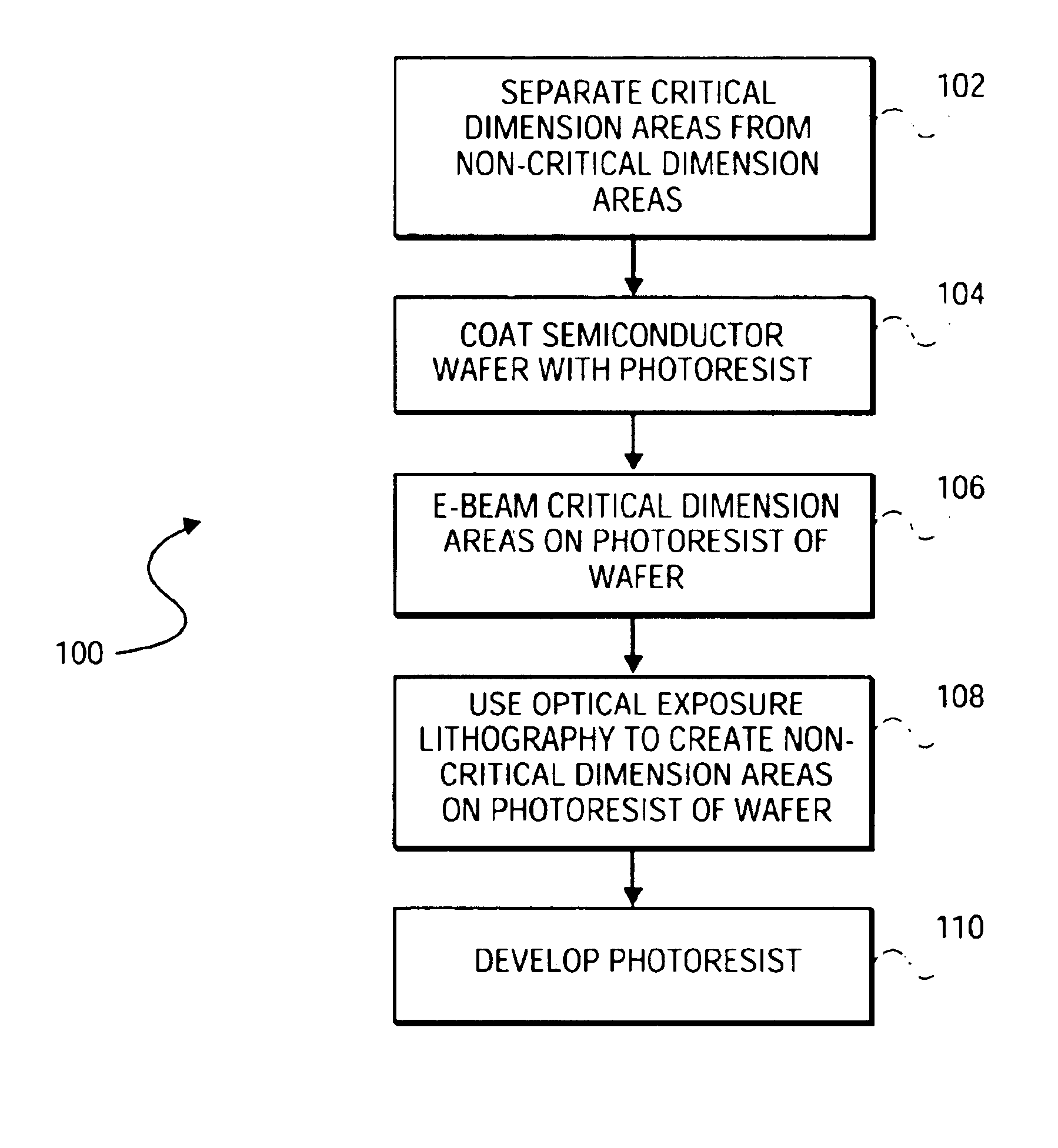
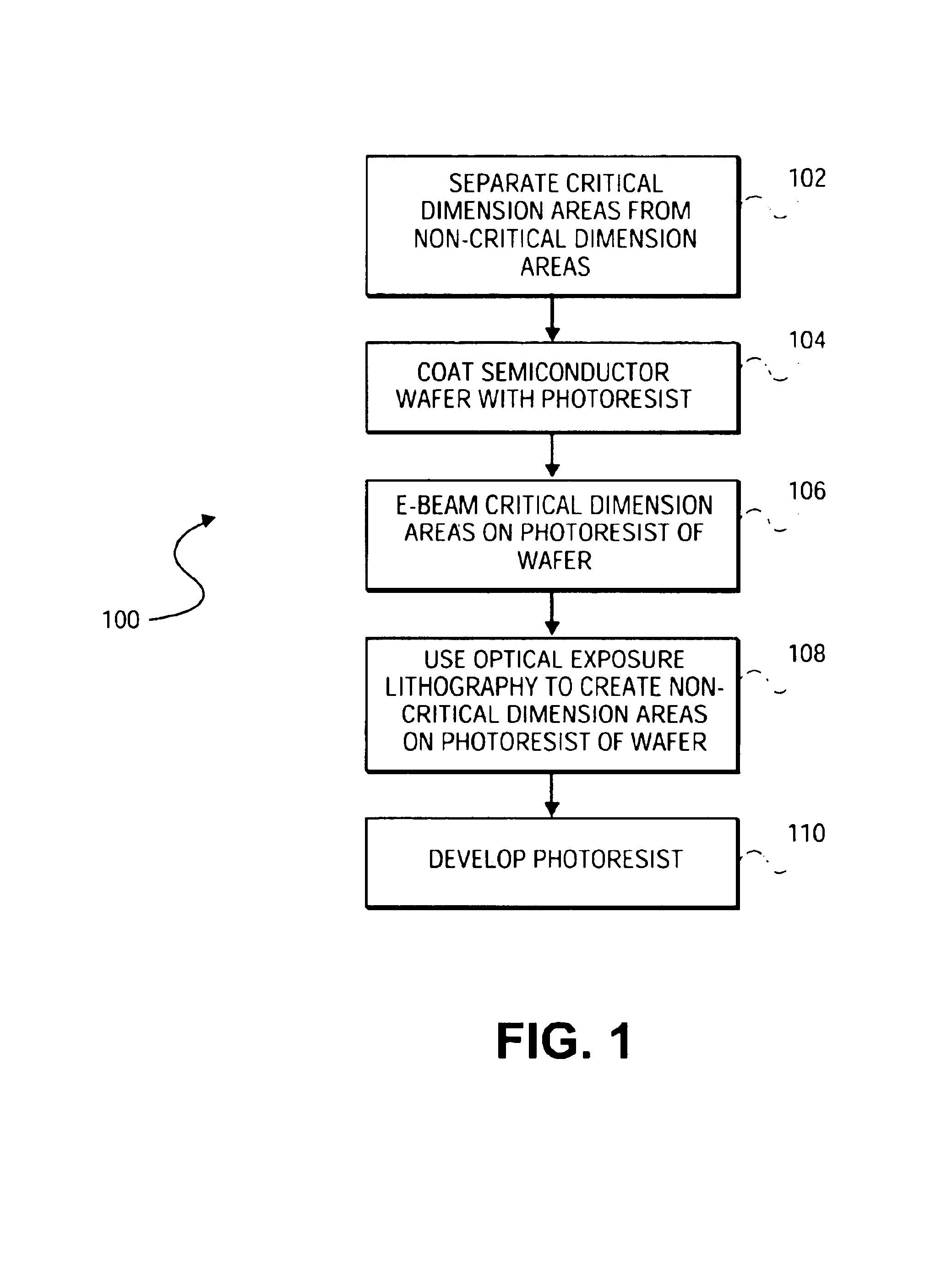
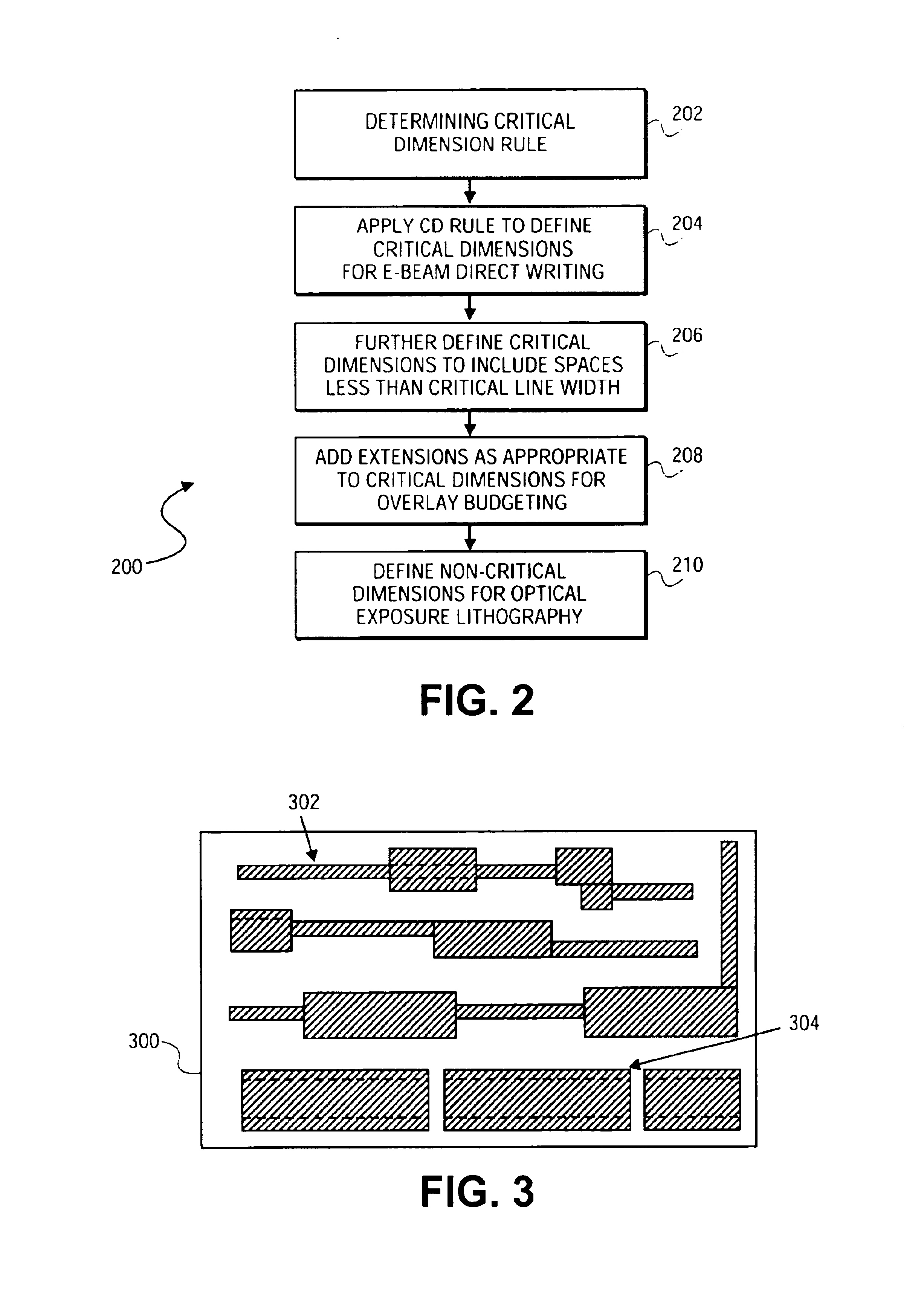
Combined E-beam and optical exposure semiconductor lithography
PatentInactiveUS6875624B2
Innovation
- A combined e-beam and optical exposure lithography method where critical dimension areas are written using precise e-beam direct writing, while non-critical dimension areas are processed with faster optical exposure lithography, separating these areas before transfer to the semiconductor wafer to achieve high resolution and throughput.

Method for improved lithographic patterning utilizing multiple coherency optimized exposures and high transmission attenuated PSM
PatentInactiveUS20050186491A1
Innovation
- The method employs high transmission attenuated phase-shift masks with optimized illumination and diffraction pattern engineering to selectively capture spatial frequency components, allowing for features with pitches much less than the exposure wavelength and near 1:1 pitch ratios, using a single reticle and multiple exposures with different coherency conditions to enhance resolution without the drawbacks of multiple reticle techniques.


Optical Design Optimization Strategies
Optical design optimization represents a critical pathway for mitigating diffraction effects in advanced photolithography systems. The fundamental approach involves refining the configuration and parameters of optical elements within the exposure system to achieve superior imaging performance. Modern computational lithography techniques enable systematic optimization of lens designs, illumination configurations, and pupil filtering strategies to counteract diffraction-induced resolution limitations.
Advanced lens design methodologies focus on minimizing aberrations while maximizing numerical aperture capabilities. High-NA immersion lithography systems employ sophisticated multi-element lens assemblies with aspherical surfaces and specialized optical materials to extend resolution boundaries. Computational optimization algorithms iteratively adjust lens curvatures, element spacing, and material selections to achieve optimal modulation transfer functions across the entire exposure field. These designs must balance competing requirements of resolution enhancement, depth of focus maintenance, and telecentricity preservation.
Illumination source optimization constitutes another essential strategy for diffraction management. Off-axis illumination techniques, including annular, dipole, and quadrupole configurations, strategically manipulate the angular distribution of incident light to enhance contrast for specific pattern orientations. Source-mask optimization algorithms co-design illumination pupil shapes alongside mask patterns, exploiting diffraction physics to improve pattern fidelity. Freeform illumination sources with customized intensity distributions enable pattern-specific optimization, though at increased computational complexity.
Pupil filtering and apodization techniques provide additional degrees of freedom for diffraction control. Phase-shifting pupil filters introduce controlled phase variations across the exit pupil to reshape point spread functions and suppress sidelobe artifacts. Amplitude apodization modulates transmission profiles to optimize the trade-off between resolution and contrast. Polarization pupil engineering exploits vectorial diffraction effects, utilizing polarization-selective elements to enhance imaging performance for high-NA systems where scalar diffraction approximations break down.
Computational co-optimization frameworks integrate multiple optical design parameters simultaneously, leveraging machine learning algorithms and inverse design methodologies to explore vast solution spaces efficiently. These holistic approaches consider system-level interactions between illumination, mask, and projection optics to identify globally optimal configurations that traditional sequential optimization methods might overlook.
Resolution Enhancement Techniques Integration
Resolution Enhancement Techniques (RET) integration represents a comprehensive approach to overcoming diffraction-induced limitations in photolithography by combining multiple complementary technologies into cohesive manufacturing workflows. The integration strategy focuses on synergizing optical proximity correction (OPC), phase-shifting masks (PSM), off-axis illumination (OAI), and computational lithography methods to achieve pattern fidelity beyond conventional optical limits. This holistic framework enables semiconductor manufacturers to extend the operational lifespan of existing lithography equipment while maintaining cost-effectiveness and production throughput.
The integration process begins with computational modeling that simultaneously optimizes multiple RET parameters. Advanced algorithms evaluate trade-offs between mask complexity, illumination configurations, and process window margins to identify optimal combinations for specific design patterns. Source-mask optimization (SMO) exemplifies this integrated approach by co-designing illumination sources and mask patterns, achieving resolution improvements that neither technique could deliver independently. This computational foundation ensures that integrated RET solutions address real manufacturing constraints rather than theoretical ideals.
Practical implementation requires careful orchestration of mask fabrication technologies and exposure system capabilities. Modern photomask production facilities must accommodate complex features including attenuated PSM structures, sub-resolution assist features (SRAF), and intricate OPC geometries within single reticles. The manufacturing tolerance stack becomes increasingly critical as multiple enhancement techniques interact, necessitating rigorous process control and metrology systems. Mask inspection technologies must detect defects across multiple enhancement layers while distinguishing intentional sub-resolution features from genuine errors.
The integration extends into exposure tool configuration and process recipe development. Scanner settings including numerical aperture, illumination pupil shapes, and dose modulation must align with mask design specifications. Process engineers develop customized exposure recipes that balance competing requirements such as depth of focus, critical dimension uniformity, and overlay accuracy. Resist chemistry selection becomes integral to RET integration, as photoresist performance directly impacts the effectiveness of optical enhancements.
Manufacturing scalability presents ongoing challenges for RET integration. Mask data preparation times increase substantially with integrated enhancement techniques, requiring high-performance computing infrastructure and optimized software algorithms. The economic viability depends on balancing enhanced resolution capabilities against increased mask costs, longer turnaround times, and computational resource requirements, making strategic technology selection essential for sustainable implementation.
Unlock deeper insights with Patsnap Eureka Quick Research — get a full tech report to explore trends and direct your research. Try now!
Generate Your Research Report Instantly with AI Agent
Supercharge your innovation with Patsnap Eureka AI Agent Platform!