

How to Integrate Sensors Using Microtransfer Printing Techniques
APR 23, 20269 MIN READ
Generate Your Research Report Instantly with AI Agent
PatSnap Eureka helps you evaluate technical feasibility & market potential.
Microtransfer Printing Technology Background and Objectives
Microtransfer printing represents a revolutionary manufacturing technique that emerged from the convergence of semiconductor processing and flexible electronics development. This technology originated in the early 2000s as researchers sought methods to transfer high-performance materials from their native growth substrates to diverse target surfaces with unprecedented precision and control.
The fundamental principle involves the selective pickup and placement of micro-scale materials using elastomeric stamps, typically composed of polydimethylsiloxane (PDMS). Unlike conventional printing methods, microtransfer printing enables the deterministic assembly of heterogeneous materials across different substrate types, including flexible, curved, and temperature-sensitive surfaces that would otherwise be incompatible with traditional semiconductor processing.
The technology has evolved through several distinct phases, beginning with basic material transfer demonstrations to sophisticated multi-material integration platforms. Early developments focused on transferring simple semiconductor structures, while contemporary applications encompass complex sensor arrays, photonic devices, and multi-functional electronic systems.
Current objectives center on achieving seamless sensor integration through enhanced transfer fidelity, improved material compatibility, and scalable manufacturing processes. Key technical goals include developing transfer mechanisms that preserve sensor functionality while enabling integration onto unconventional substrates such as biological tissues, curved surfaces, and flexible polymer films.
The primary challenge lies in maintaining electrical connectivity and mechanical integrity during the transfer process while ensuring optimal sensor performance post-integration. Advanced stamp designs, interface engineering, and process optimization represent critical focus areas for achieving reliable sensor integration.
Strategic objectives encompass expanding the range of transferable sensor types, from traditional silicon-based devices to emerging two-dimensional materials and organic semiconductors. The technology aims to enable distributed sensor networks with unprecedented form factors and deployment flexibility, particularly for applications in wearable electronics, biomedical devices, and Internet of Things systems.
Future development trajectories target automated high-throughput transfer systems, real-time process monitoring capabilities, and integration with advanced packaging technologies to create complete sensor solutions ready for commercial deployment across diverse application domains.
The fundamental principle involves the selective pickup and placement of micro-scale materials using elastomeric stamps, typically composed of polydimethylsiloxane (PDMS). Unlike conventional printing methods, microtransfer printing enables the deterministic assembly of heterogeneous materials across different substrate types, including flexible, curved, and temperature-sensitive surfaces that would otherwise be incompatible with traditional semiconductor processing.
The technology has evolved through several distinct phases, beginning with basic material transfer demonstrations to sophisticated multi-material integration platforms. Early developments focused on transferring simple semiconductor structures, while contemporary applications encompass complex sensor arrays, photonic devices, and multi-functional electronic systems.
Current objectives center on achieving seamless sensor integration through enhanced transfer fidelity, improved material compatibility, and scalable manufacturing processes. Key technical goals include developing transfer mechanisms that preserve sensor functionality while enabling integration onto unconventional substrates such as biological tissues, curved surfaces, and flexible polymer films.
The primary challenge lies in maintaining electrical connectivity and mechanical integrity during the transfer process while ensuring optimal sensor performance post-integration. Advanced stamp designs, interface engineering, and process optimization represent critical focus areas for achieving reliable sensor integration.
Strategic objectives encompass expanding the range of transferable sensor types, from traditional silicon-based devices to emerging two-dimensional materials and organic semiconductors. The technology aims to enable distributed sensor networks with unprecedented form factors and deployment flexibility, particularly for applications in wearable electronics, biomedical devices, and Internet of Things systems.
Future development trajectories target automated high-throughput transfer systems, real-time process monitoring capabilities, and integration with advanced packaging technologies to create complete sensor solutions ready for commercial deployment across diverse application domains.
Market Demand for Advanced Sensor Integration Solutions
The global sensor market is experiencing unprecedented growth driven by the proliferation of Internet of Things applications, autonomous vehicles, healthcare monitoring systems, and industrial automation. Traditional sensor integration methods face significant limitations in terms of miniaturization, flexibility, and manufacturing scalability, creating substantial market opportunities for advanced integration solutions.
Microtransfer printing techniques address critical market demands for heterogeneous sensor integration on flexible substrates and unconventional surfaces. The wearable electronics sector represents a particularly compelling market segment, where consumers and healthcare providers increasingly require seamless integration of multiple sensing modalities including temperature, pressure, strain, and biochemical sensors on skin-conformable platforms.
The automotive industry demonstrates strong demand for advanced sensor integration solutions to support autonomous driving capabilities. Current challenges in integrating diverse sensor types such as LiDAR, cameras, radar, and environmental sensors onto vehicle surfaces create opportunities for microtransfer printing technologies to enable more efficient and cost-effective sensor deployment strategies.
Industrial Internet of Things applications require distributed sensor networks capable of monitoring multiple parameters simultaneously across manufacturing environments. Microtransfer printing enables the integration of sensors onto irregular surfaces, machinery components, and infrastructure elements where traditional mounting approaches prove inadequate or economically unfeasible.
Healthcare and biomedical applications represent rapidly expanding market segments demanding minimally invasive sensor integration solutions. The ability to transfer sensors onto biocompatible substrates and medical devices opens new possibilities for continuous patient monitoring, diagnostic applications, and therapeutic interventions that require precise sensor placement and integration.
The consumer electronics market increasingly demands thinner, lighter devices with enhanced sensing capabilities. Microtransfer printing techniques enable manufacturers to integrate sensors into space-constrained environments while maintaining device aesthetics and functionality, addressing consumer preferences for sleek, multifunctional electronic products.
Emerging applications in smart infrastructure, environmental monitoring, and aerospace systems further expand market opportunities. These sectors require sensor integration solutions capable of operating in harsh environments while maintaining reliability and performance standards that traditional integration methods struggle to achieve consistently.
Microtransfer printing techniques address critical market demands for heterogeneous sensor integration on flexible substrates and unconventional surfaces. The wearable electronics sector represents a particularly compelling market segment, where consumers and healthcare providers increasingly require seamless integration of multiple sensing modalities including temperature, pressure, strain, and biochemical sensors on skin-conformable platforms.
The automotive industry demonstrates strong demand for advanced sensor integration solutions to support autonomous driving capabilities. Current challenges in integrating diverse sensor types such as LiDAR, cameras, radar, and environmental sensors onto vehicle surfaces create opportunities for microtransfer printing technologies to enable more efficient and cost-effective sensor deployment strategies.
Industrial Internet of Things applications require distributed sensor networks capable of monitoring multiple parameters simultaneously across manufacturing environments. Microtransfer printing enables the integration of sensors onto irregular surfaces, machinery components, and infrastructure elements where traditional mounting approaches prove inadequate or economically unfeasible.
Healthcare and biomedical applications represent rapidly expanding market segments demanding minimally invasive sensor integration solutions. The ability to transfer sensors onto biocompatible substrates and medical devices opens new possibilities for continuous patient monitoring, diagnostic applications, and therapeutic interventions that require precise sensor placement and integration.
The consumer electronics market increasingly demands thinner, lighter devices with enhanced sensing capabilities. Microtransfer printing techniques enable manufacturers to integrate sensors into space-constrained environments while maintaining device aesthetics and functionality, addressing consumer preferences for sleek, multifunctional electronic products.
Emerging applications in smart infrastructure, environmental monitoring, and aerospace systems further expand market opportunities. These sectors require sensor integration solutions capable of operating in harsh environments while maintaining reliability and performance standards that traditional integration methods struggle to achieve consistently.
Current State and Challenges in Microtransfer Printing
Microtransfer printing has emerged as a promising technique for heterogeneous integration of diverse materials and devices, particularly in sensor applications. Currently, the technology demonstrates significant capabilities in transferring thin semiconductor membranes, nanowires, and micro-scale devices from donor substrates to receiver substrates with high precision. Leading research institutions and companies have successfully demonstrated transfer of various sensor components including photodetectors, strain gauges, and chemical sensors onto flexible and rigid substrates.
The state-of-the-art microtransfer printing processes typically achieve transfer yields exceeding 95% for devices larger than 10 micrometers, with positioning accuracies reaching sub-micrometer levels. Advanced elastomeric stamps, particularly those based on polydimethylsiloxane (PDMS) and its derivatives, enable selective pickup and placement of devices through controlled adhesion mechanisms. Recent developments have expanded the technique's capability to handle devices ranging from nanoscale components to millimeter-sized sensors.
Despite these advances, several critical challenges persist in implementing microtransfer printing for sensor integration. Adhesion control remains a fundamental obstacle, as the process requires precise modulation of interfacial forces between the stamp, device, and target substrate. The kinetic control of pickup and release processes often lacks consistency, particularly when dealing with devices of varying sizes and materials within the same transfer operation.
Thermal and mechanical stress management presents another significant challenge. During transfer processes, temperature variations and mechanical deformation can compromise sensor performance and reliability. The mismatch in thermal expansion coefficients between different materials often leads to residual stresses that affect sensor accuracy and long-term stability.
Scalability issues limit widespread adoption of microtransfer printing in sensor manufacturing. Current processes are predominantly laboratory-scale demonstrations, with limited throughput and reproducibility for industrial applications. The alignment precision required for multi-sensor integration becomes increasingly difficult as device density increases, particularly in applications requiring electrical interconnections between transferred components.
Electrical connectivity establishment after device transfer poses substantial technical hurdles. Traditional wire bonding and lithographic interconnection methods often prove incompatible with the delicate nature of transferred sensors. The development of reliable, low-resistance electrical contacts without damaging the transferred devices remains an active area of research.
Material compatibility constraints further complicate sensor integration efforts. Many sensor materials exhibit poor adhesion characteristics with standard elastomeric stamps, while others may be damaged by the chemical interactions during the transfer process. The limited availability of suitable release layers and the need for surface treatments add complexity to the overall integration workflow.
The state-of-the-art microtransfer printing processes typically achieve transfer yields exceeding 95% for devices larger than 10 micrometers, with positioning accuracies reaching sub-micrometer levels. Advanced elastomeric stamps, particularly those based on polydimethylsiloxane (PDMS) and its derivatives, enable selective pickup and placement of devices through controlled adhesion mechanisms. Recent developments have expanded the technique's capability to handle devices ranging from nanoscale components to millimeter-sized sensors.
Despite these advances, several critical challenges persist in implementing microtransfer printing for sensor integration. Adhesion control remains a fundamental obstacle, as the process requires precise modulation of interfacial forces between the stamp, device, and target substrate. The kinetic control of pickup and release processes often lacks consistency, particularly when dealing with devices of varying sizes and materials within the same transfer operation.
Thermal and mechanical stress management presents another significant challenge. During transfer processes, temperature variations and mechanical deformation can compromise sensor performance and reliability. The mismatch in thermal expansion coefficients between different materials often leads to residual stresses that affect sensor accuracy and long-term stability.
Scalability issues limit widespread adoption of microtransfer printing in sensor manufacturing. Current processes are predominantly laboratory-scale demonstrations, with limited throughput and reproducibility for industrial applications. The alignment precision required for multi-sensor integration becomes increasingly difficult as device density increases, particularly in applications requiring electrical interconnections between transferred components.
Electrical connectivity establishment after device transfer poses substantial technical hurdles. Traditional wire bonding and lithographic interconnection methods often prove incompatible with the delicate nature of transferred sensors. The development of reliable, low-resistance electrical contacts without damaging the transferred devices remains an active area of research.
Material compatibility constraints further complicate sensor integration efforts. Many sensor materials exhibit poor adhesion characteristics with standard elastomeric stamps, while others may be damaged by the chemical interactions during the transfer process. The limited availability of suitable release layers and the need for surface treatments add complexity to the overall integration workflow.
Existing Microtransfer Printing Integration Methods
01 Stamp-based transfer printing methods
Microtransfer printing techniques utilizing elastomeric stamps or molds to pick up and transfer micro-scale materials from donor substrates to receiver substrates. The stamp makes conformal contact with the source material, allowing selective retrieval and precise placement of thin films, patterns, or device components through controlled adhesion and release mechanisms.- Stamp-based transfer printing methods: Microtransfer printing techniques utilizing elastomeric stamps or molds to pick up and transfer micro-scale materials, structures, or patterns from a donor substrate to a receiving substrate. The stamp makes conformal contact with the source material and selectively adheres to transfer the desired elements through controlled adhesion and release mechanisms. This approach enables precise positioning and patterning of microscale components including semiconductors, metals, and organic materials.
- Ink formulation and material composition for transfer: Development of specialized ink compositions and material formulations optimized for microtransfer printing processes. These formulations include considerations for viscosity, adhesion properties, curing characteristics, and compatibility with both stamp materials and target substrates. The compositions may incorporate nanoparticles, conductive materials, polymers, or functional additives that enable effective transfer and subsequent processing of printed features.
- Alignment and registration systems: Precision alignment and registration mechanisms for achieving accurate positioning during microtransfer printing operations. These systems employ optical detection, mechanical guides, or automated control systems to ensure proper alignment between stamps, donor substrates, and receiving substrates. The techniques enable multi-layer printing with high registration accuracy necessary for complex device fabrication and pattern overlay applications.
- Surface treatment and adhesion control: Methods for controlling surface properties and adhesion characteristics to facilitate selective transfer in microtransfer printing. Surface treatments may include chemical modification, plasma treatment, or application of release layers to modulate interfacial adhesion between stamps, source materials, and target substrates. These techniques enable controlled pick-up and release of transferred materials while preventing contamination or damage.
- Applications in electronic device fabrication: Implementation of microtransfer printing techniques for manufacturing electronic devices and components. Applications include fabrication of thin-film transistors, flexible displays, sensors, photovoltaic devices, and integrated circuits. The technology enables heterogeneous integration of different materials and components, assembly of flexible and stretchable electronics, and cost-effective production of micro and nanoscale electronic structures on various substrate types.
02 Ink formulation and material compatibility
Development of specialized inks and material systems optimized for microtransfer printing processes. This includes formulations with appropriate viscosity, surface tension, and adhesion properties that enable effective transfer from donor to receiver substrates. The materials must maintain structural integrity during the printing process while achieving strong bonding to the final substrate.Expand Specific Solutions03 Alignment and registration systems
Precision alignment mechanisms and registration techniques for accurate positioning during microtransfer printing. These systems employ optical detection, mechanical guides, or automated control systems to ensure proper placement of transferred materials with micrometer or sub-micrometer accuracy, critical for multi-layer device fabrication and pattern overlay.Expand Specific Solutions04 Applications in electronic device fabrication
Implementation of microtransfer printing for manufacturing electronic components and displays. This approach enables heterogeneous integration of different materials and devices, including thin-film transistors, light-emitting diodes, and sensor arrays, onto various substrates including flexible and unconventional surfaces that cannot withstand traditional processing conditions.Expand Specific Solutions05 Surface treatment and adhesion control
Methods for controlling interfacial adhesion between stamps, source materials, and target substrates through surface modifications. Techniques include plasma treatment, chemical functionalization, and application of adhesion-promoting or release layers to optimize the pick-up and printing steps, ensuring high transfer yield and pattern fidelity.Expand Specific Solutions
Key Players in Microtransfer Printing Industry
The microtransfer printing technology for sensor integration represents an emerging field in the early commercialization stage, with significant growth potential driven by increasing demand for flexible electronics and IoT applications. The market remains relatively nascent but shows promising expansion across automotive, healthcare, and consumer electronics sectors. Technology maturity varies considerably among key players, with X Display Co. Technology Ltd. leading as a specialized pioneer in micro-transfer-printing techniques, while established semiconductor giants like Apple, Taiwan Semiconductor Manufacturing, Texas Instruments, and Infineon Technologies leverage their manufacturing expertise to integrate these capabilities. Research institutions including University of Illinois, Ghent University, and Jiangnan University contribute foundational innovations, while companies like BOE Technology, Seiko Epson, and Philips explore commercial applications in display and healthcare sectors, indicating a competitive landscape characterized by both specialized startups and diversified technology corporations pursuing different market entry strategies.
The Board of Trustees of the University of Illinois
Technical Solution: The University of Illinois has pioneered fundamental microtransfer printing technologies, particularly focusing on the development of PDMS-based elastomeric stamps for sensor integration. Their research encompasses the use of kinetically controlled adhesion mechanisms where the rate of contact and separation determines the transfer efficiency. The university has developed techniques for transferring various sensor components including silicon nanomembranes, III-V compound semiconductors, and organic electronic materials. Their approach utilizes surface chemistry modifications and controlled interfacial adhesion to achieve selective transfer of sensors from growth substrates to flexible or rigid receiver substrates, enabling heterogeneous integration of different sensor technologies on a single platform.
Strengths: Strong fundamental research foundation, innovative material approaches, excellent academic collaboration network. Weaknesses: Limited commercial scalability, primarily research-focused rather than production-ready, longer development timelines.
Apple, Inc.
Technical Solution: Apple has developed advanced microtransfer printing techniques for integrating micro-LED displays and sensors into their devices. Their approach utilizes selective adhesion and release mechanisms to transfer microscale components from donor substrates to receiver substrates with high precision. The company employs elastomeric stamps with controlled surface energy to achieve selective pickup and placement of sensors, enabling the integration of multiple sensor types including accelerometers, gyroscopes, and ambient light sensors into compact form factors. Apple's microtransfer printing process incorporates temperature-controlled release mechanisms and uses specialized adhesive layers that can be selectively activated or deactivated during the transfer process.
Strengths: High precision placement accuracy, excellent yield rates for consumer electronics applications, proven scalability for mass production. Weaknesses: Limited to specific sensor types, high equipment costs, proprietary technology with limited accessibility.
Core Patents in Microtransfer Printing Sensor Integration
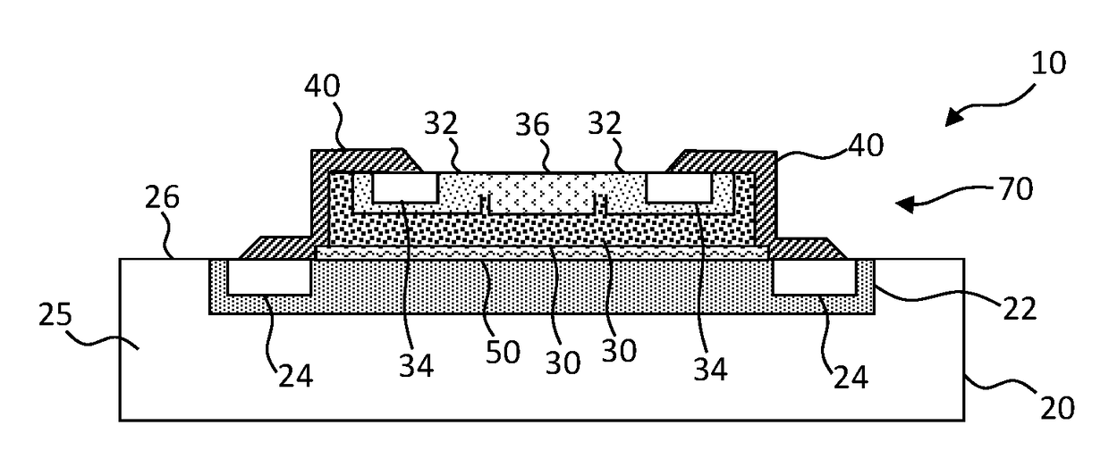
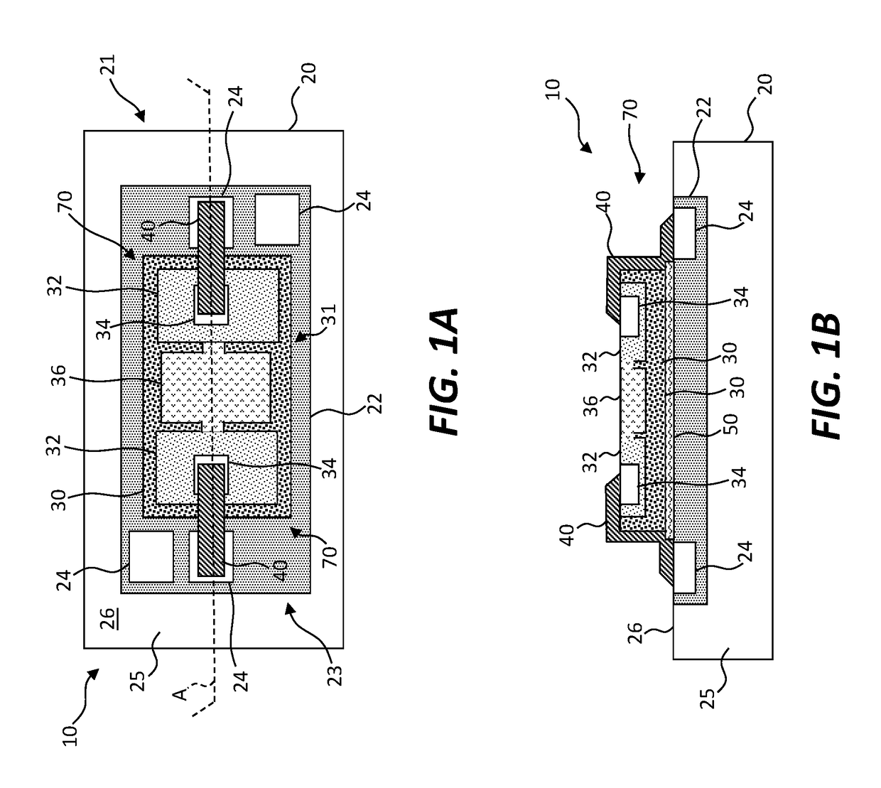
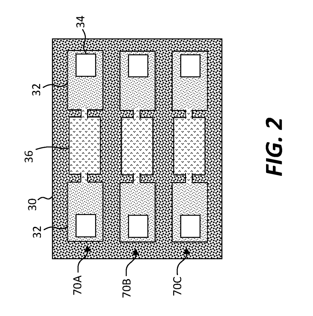
Micro-transfer-printed compound sensor device
PatentActiveUS20170225945A1
Innovation
- A compound sensor device is created by micro-transfer printing a sensor substrate with a different material and technology onto a semiconductor substrate, reducing the length of electrical connections and enabling better integration and performance, particularly in high-frequency applications.

Micro-transfer printing with selective component removal
PatentActiveUS20200335380A1
Innovation
- The method employs a micro-transfer printing system using a visco-elastic stamp with spatially distributed posts that selectively adhere and detach micro-devices through controlled light irradiation, allowing for the precise transfer of selected components from a source wafer to a destination substrate while leaving non-selected components behind.


Manufacturing Standards for Microtransfer Processes
The establishment of comprehensive manufacturing standards for microtransfer processes represents a critical foundation for the successful integration of sensors through microtransfer printing techniques. Current industry practices reveal significant variations in process parameters, quality metrics, and validation protocols across different manufacturers and research institutions. This lack of standardization creates barriers to scalable production and limits the widespread adoption of microtransfer printing for sensor integration applications.
Process parameter standardization encompasses several key areas including substrate preparation specifications, ink formulation guidelines, and printing environment controls. Temperature and humidity tolerances must be precisely defined, typically requiring cleanroom conditions with temperature stability within ±2°C and relative humidity maintained between 40-60%. Substrate surface energy requirements need standardization, with most successful implementations requiring surface energies between 40-60 mN/m for optimal ink adhesion and pattern fidelity.
Quality control standards for microtransfer processes demand rigorous measurement protocols and acceptance criteria. Feature resolution standards typically specify minimum line widths of 10-50 micrometers depending on the sensor application, with edge roughness tolerances not exceeding 10% of the feature width. Registration accuracy between multiple printing layers must maintain alignment within ±5 micrometers to ensure proper sensor functionality and electrical connectivity.
Equipment calibration and maintenance standards play a crucial role in ensuring consistent manufacturing outcomes. Print head alignment procedures require standardized calibration protocols performed at regular intervals, typically every 100 operating hours or after substrate changes. Ink delivery system maintenance standards must address viscosity monitoring, nozzle cleaning procedures, and pressure regulation to maintain consistent droplet formation and placement accuracy.
Material qualification standards establish requirements for both substrate materials and functional inks used in sensor integration. Substrate specifications must address thermal expansion coefficients, surface roughness parameters, and chemical compatibility with processing solvents. Functional ink standards need to define particle size distributions, rheological properties, and shelf-life requirements to ensure reproducible printing performance and long-term sensor reliability.
Documentation and traceability standards ensure manufacturing consistency and enable continuous process improvement. Batch tracking requirements mandate comprehensive recording of process parameters, environmental conditions, and quality measurements for each production run. These standards facilitate root cause analysis when quality issues arise and support the development of predictive maintenance protocols for manufacturing equipment.
Process parameter standardization encompasses several key areas including substrate preparation specifications, ink formulation guidelines, and printing environment controls. Temperature and humidity tolerances must be precisely defined, typically requiring cleanroom conditions with temperature stability within ±2°C and relative humidity maintained between 40-60%. Substrate surface energy requirements need standardization, with most successful implementations requiring surface energies between 40-60 mN/m for optimal ink adhesion and pattern fidelity.
Quality control standards for microtransfer processes demand rigorous measurement protocols and acceptance criteria. Feature resolution standards typically specify minimum line widths of 10-50 micrometers depending on the sensor application, with edge roughness tolerances not exceeding 10% of the feature width. Registration accuracy between multiple printing layers must maintain alignment within ±5 micrometers to ensure proper sensor functionality and electrical connectivity.
Equipment calibration and maintenance standards play a crucial role in ensuring consistent manufacturing outcomes. Print head alignment procedures require standardized calibration protocols performed at regular intervals, typically every 100 operating hours or after substrate changes. Ink delivery system maintenance standards must address viscosity monitoring, nozzle cleaning procedures, and pressure regulation to maintain consistent droplet formation and placement accuracy.
Material qualification standards establish requirements for both substrate materials and functional inks used in sensor integration. Substrate specifications must address thermal expansion coefficients, surface roughness parameters, and chemical compatibility with processing solvents. Functional ink standards need to define particle size distributions, rheological properties, and shelf-life requirements to ensure reproducible printing performance and long-term sensor reliability.
Documentation and traceability standards ensure manufacturing consistency and enable continuous process improvement. Batch tracking requirements mandate comprehensive recording of process parameters, environmental conditions, and quality measurements for each production run. These standards facilitate root cause analysis when quality issues arise and support the development of predictive maintenance protocols for manufacturing equipment.
Scalability and Cost Analysis of Microtransfer Solutions
The scalability of microtransfer printing techniques for sensor integration presents both significant opportunities and challenges across different production volumes. At laboratory and prototype scales, the technology demonstrates excellent precision and flexibility, enabling the integration of diverse sensor types including photodetectors, strain gauges, and chemical sensors onto various substrates. However, transitioning from research-scale demonstrations to industrial manufacturing requires substantial infrastructure investments and process optimization.
Manufacturing scalability primarily depends on throughput capabilities and yield consistency. Current microtransfer printing systems can achieve transfer rates of several hundred devices per hour, which is adequate for specialized applications but insufficient for consumer electronics requiring millions of units. The parallel processing approach, where multiple sensors are transferred simultaneously, offers potential solutions but introduces complexity in alignment accuracy and uniformity control across large substrate areas.
Cost analysis reveals that equipment capital expenditure represents the most significant barrier to widespread adoption. High-precision microtransfer printing systems typically cost between $2-5 million, with additional expenses for clean room facilities and specialized tooling. The cost per transferred device decreases substantially with volume, dropping from approximately $10-50 per sensor at prototype scales to potentially under $1 at high-volume production, assuming optimized processes and equipment utilization.
Material costs contribute significantly to overall expenses, particularly for high-performance sensor materials and specialized adhesives required for reliable transfer. The donor substrate preparation and handling represent recurring costs that scale linearly with production volume. Advanced materials like III-V semiconductors for optical sensors can account for 30-60% of total manufacturing costs, making material utilization efficiency critical for economic viability.
Process yield directly impacts economic feasibility, with current laboratory demonstrations achieving 85-95% transfer success rates. Industrial applications require yields exceeding 99.5% to maintain cost competitiveness with conventional assembly methods. Defect sources include alignment errors, contamination, and mechanical damage during transfer, each requiring specific mitigation strategies that may increase process complexity and costs.
The economic break-even point for microtransfer printing typically occurs at production volumes exceeding 100,000 units annually for specialized applications, while consumer applications may require volumes above one million units to achieve cost parity with traditional packaging methods.
Manufacturing scalability primarily depends on throughput capabilities and yield consistency. Current microtransfer printing systems can achieve transfer rates of several hundred devices per hour, which is adequate for specialized applications but insufficient for consumer electronics requiring millions of units. The parallel processing approach, where multiple sensors are transferred simultaneously, offers potential solutions but introduces complexity in alignment accuracy and uniformity control across large substrate areas.
Cost analysis reveals that equipment capital expenditure represents the most significant barrier to widespread adoption. High-precision microtransfer printing systems typically cost between $2-5 million, with additional expenses for clean room facilities and specialized tooling. The cost per transferred device decreases substantially with volume, dropping from approximately $10-50 per sensor at prototype scales to potentially under $1 at high-volume production, assuming optimized processes and equipment utilization.
Material costs contribute significantly to overall expenses, particularly for high-performance sensor materials and specialized adhesives required for reliable transfer. The donor substrate preparation and handling represent recurring costs that scale linearly with production volume. Advanced materials like III-V semiconductors for optical sensors can account for 30-60% of total manufacturing costs, making material utilization efficiency critical for economic viability.
Process yield directly impacts economic feasibility, with current laboratory demonstrations achieving 85-95% transfer success rates. Industrial applications require yields exceeding 99.5% to maintain cost competitiveness with conventional assembly methods. Defect sources include alignment errors, contamination, and mechanical damage during transfer, each requiring specific mitigation strategies that may increase process complexity and costs.
The economic break-even point for microtransfer printing typically occurs at production volumes exceeding 100,000 units annually for specialized applications, while consumer applications may require volumes above one million units to achieve cost parity with traditional packaging methods.
Unlock deeper insights with PatSnap Eureka Quick Research — get a full tech report to explore trends and direct your research. Try now!
Generate Your Research Report Instantly with AI Agent
Supercharge your innovation with PatSnap Eureka AI Agent Platform!