

How to Leverage Microtransfer Printing for Nanostructures
APR 23, 20268 MIN READ
Generate Your Research Report Instantly with AI Agent
Patsnap Eureka helps you evaluate technical feasibility & market potential.
Microtransfer Printing Technology Background and Objectives
Microtransfer printing represents a revolutionary nanofabrication technique that has emerged as a critical enabler for advanced nanostructure manufacturing and assembly. This technology originated from the fundamental need to overcome the limitations of traditional lithographic processes, particularly in achieving high-resolution patterning across large areas while maintaining cost-effectiveness and material compatibility. The technique leverages elastomeric stamps to selectively retrieve and deposit nanostructures from donor substrates to receiver substrates with exceptional precision and control.
The historical development of microtransfer printing can be traced back to early soft lithography concepts, evolving through significant breakthroughs in stamp material engineering and process optimization. Initial implementations focused on transferring simple geometric patterns, but the technology has progressively advanced to handle complex three-dimensional nanostructures, including quantum dots, nanowires, and sophisticated semiconductor devices. This evolution has been driven by the increasing demand for heterogeneous integration in electronics, photonics, and biomedical applications.
Current technological trends indicate a strong momentum toward achieving sub-10-nanometer resolution capabilities while expanding the range of transferable materials. The integration of advanced elastomer chemistries, surface functionalization techniques, and real-time process monitoring systems has significantly enhanced the reliability and reproducibility of the transfer process. These developments have positioned microtransfer printing as a viable alternative to conventional pick-and-place methods for nanostructure assembly.
The primary objective of leveraging microtransfer printing for nanostructures centers on achieving deterministic assembly of heterogeneous materials with nanoscale precision. This includes enabling the integration of dissimilar materials that cannot be co-processed using traditional fabrication methods, facilitating the creation of complex device architectures that combine multiple functional elements. The technology aims to bridge the gap between bottom-up synthesis of nanostructures and top-down device fabrication, offering unprecedented flexibility in material selection and device design.
Strategic goals encompass scaling the technology for industrial manufacturing while maintaining the inherent advantages of selective transfer and material preservation. The ultimate vision involves establishing microtransfer printing as a standard manufacturing platform capable of producing next-generation electronic, photonic, and sensing devices with enhanced performance characteristics and reduced manufacturing complexity.
Market Demand for Nanostructure Manufacturing Solutions
The global nanostructure manufacturing market is experiencing unprecedented growth driven by the convergence of multiple high-tech industries demanding precise, scalable fabrication solutions. Semiconductor manufacturers are increasingly requiring advanced packaging technologies that can handle heterogeneous integration of diverse materials and components at nanoscale dimensions. The transition toward more-than-Moore scaling strategies has created substantial demand for manufacturing processes capable of transferring delicate nanostructures with sub-micron precision across different substrate materials.
Consumer electronics represent a particularly robust demand segment, where the miniaturization of displays, sensors, and processing units necessitates manufacturing techniques that can handle fragile nanostructures without compromising their functional properties. The proliferation of flexible electronics, wearable devices, and Internet of Things applications has further amplified the need for manufacturing solutions that can transfer nanostructures onto unconventional substrates including flexible polymers and curved surfaces.
The biomedical sector presents another significant growth driver, with increasing applications in biosensors, drug delivery systems, and diagnostic devices requiring precise placement of functional nanostructures. Medical device manufacturers are seeking manufacturing solutions that can maintain the integrity of biological interfaces while enabling mass production capabilities. The growing emphasis on personalized medicine and point-of-care diagnostics has created demand for cost-effective manufacturing processes that can produce small batches of highly specialized nanostructured devices.
Emerging applications in quantum computing, photonics, and energy harvesting are generating new market segments with specific requirements for nanostructure manufacturing. These applications often involve exotic materials and complex geometries that traditional lithographic processes cannot adequately address. The market is particularly receptive to manufacturing solutions that can handle diverse material systems including III-V semiconductors, two-dimensional materials, and hybrid organic-inorganic structures.
Manufacturing cost reduction remains a critical market driver, as industries seek alternatives to expensive cleanroom-based processes. The demand for manufacturing solutions that can operate in ambient conditions while maintaining high yield and precision continues to grow across multiple sectors.
Current State and Challenges in Microtransfer Printing
Microtransfer printing has emerged as a promising technique for fabricating nanostructures with high precision and scalability. Currently, the technology demonstrates significant capabilities in transferring nanoscale materials from donor substrates to receiver substrates using elastomeric stamps, typically made from polydimethylsiloxane (PDMS). The process enables the assembly of diverse materials including semiconductors, metals, and organic compounds into complex nanostructured devices.
The state-of-the-art microtransfer printing systems can achieve feature sizes down to sub-100 nanometer scales with reasonable throughput. Leading research institutions and companies have successfully demonstrated applications in flexible electronics, photonic devices, and biomedical sensors. The technology has shown particular promise in heterogeneous integration, allowing different material systems to be combined on a single substrate without the thermal and chemical constraints of traditional epitaxial growth methods.
Despite these advances, several critical challenges persist in the widespread adoption of microtransfer printing for nanostructures. Adhesion control remains a fundamental issue, as the process requires precise manipulation of interfacial forces between the stamp, transferred material, and target substrate. Achieving reliable and selective transfer while maintaining structural integrity of delicate nanostructures presents ongoing difficulties.
Registration accuracy poses another significant challenge, particularly for applications requiring precise alignment of multiple layers or components. Current systems struggle to achieve the sub-nanometer alignment precision demanded by advanced nanoelectronic devices. The mechanical properties of elastomeric stamps also introduce limitations, as they can deform under pressure, leading to pattern distortion and reduced transfer fidelity.
Scalability concerns affect both manufacturing throughput and uniformity across large substrate areas. While laboratory demonstrations show excellent results for small-scale patterns, maintaining consistent transfer quality over wafer-scale areas remains problematic. Process repeatability and yield optimization require further development to meet industrial manufacturing standards.
Material compatibility represents an additional constraint, as different nanostructures exhibit varying adhesion characteristics and mechanical properties. The development of universal transfer protocols that can accommodate diverse material systems while maintaining high transfer efficiency continues to challenge researchers in this field.
Existing Microtransfer Printing Solutions
01 Stamp-based transfer printing methods
This category involves the use of elastomeric stamps or molds to transfer materials from a donor substrate to a receiver substrate. The stamp makes conformal contact with the donor surface to pick up materials, then transfers them to the target substrate through controlled adhesion and release mechanisms. This approach enables precise pattern transfer and is particularly useful for transferring thin films, nanostructures, and functional materials.- Stamp-based transfer printing methods: This category involves the use of elastomeric stamps or molds to transfer materials from a donor substrate to a receiver substrate. The stamp makes conformal contact with the donor surface, picks up the material through adhesion control, and then releases it onto the target substrate. This method enables precise pattern transfer and is particularly useful for transferring thin films, nanostructures, and functional materials with high fidelity.
- Transfer printing for electronic device fabrication: This approach focuses on using transfer printing techniques to fabricate electronic devices and components. The method allows for the assembly of semiconductor materials, conductive patterns, and functional layers onto various substrates including flexible and non-conventional surfaces. This enables the creation of displays, sensors, and integrated circuits through selective material transfer and positioning.
- Adhesion control mechanisms in transfer printing: This category addresses methods for controlling adhesion between the transfer medium and substrates during the printing process. Techniques include modulating surface properties, applying pressure or temperature changes, and using release layers to enable selective pickup and release of materials. Proper adhesion control is critical for achieving high transfer yields and pattern integrity.
- Micro and nano-scale pattern transfer: This technology focuses on transferring patterns and structures at microscopic and nanoscopic scales. The methods enable the reproduction of fine features with high resolution and accuracy, suitable for applications in microelectronics, photonics, and biotechnology. The transfer process maintains the dimensional accuracy and structural integrity of small-scale features during relocation from one substrate to another.
- Substrate compatibility and material versatility: This category encompasses transfer printing methods that accommodate diverse substrate materials and geometries. The techniques allow printing onto flexible, curved, or temperature-sensitive surfaces that cannot withstand conventional processing. This versatility extends the application range to include plastic electronics, biomedical devices, and three-dimensional structures, enabling material integration across incompatible processing platforms.
02 Selective adhesion control in transfer printing
Techniques for controlling adhesion between the transfer stamp and materials during pick-up and release stages are critical for successful transfer printing. Methods include modulating stamp properties, surface treatments, temperature control, and kinetic control of peeling rates. These approaches enable selective transfer of specific materials or patterns while maintaining material integrity and achieving high transfer yields.Expand Specific Solutions03 Transfer printing for electronic device fabrication
Application of transfer printing techniques to manufacture electronic devices and components, including displays, sensors, and integrated circuits. This approach allows heterogeneous integration of materials and devices on various substrates, enabling flexible electronics, curved displays, and unconventional form factors. The method facilitates the assembly of pre-fabricated components onto target substrates without high-temperature processing.Expand Specific Solutions04 Micro and nano-scale pattern transfer
Methods for transferring microscale and nanoscale patterns and structures with high resolution and fidelity. These techniques enable the replication of fine features and complex geometries from master templates to target substrates. Applications include photonic devices, microelectromechanical systems, and nanostructured surfaces. The approach often involves optimized stamp materials and process parameters to achieve sub-micron resolution.Expand Specific Solutions05 Multi-layer and sequential transfer printing
Processes for performing multiple transfer printing steps to create multi-layer structures or complex device architectures. This includes sequential transfer of different materials, alignment techniques for layer-to-layer registration, and methods for building three-dimensional structures. The approach enables the fabrication of sophisticated devices with multiple functional layers and heterogeneous material integration.Expand Specific Solutions
Key Players in Microtransfer Printing Industry
The microtransfer printing technology for nanostructures represents an emerging field in the growth stage, with significant market potential driven by applications in semiconductors, displays, and advanced manufacturing. The global market is expanding rapidly as industries seek cost-effective methods for integrating microscale devices onto non-native substrates. Technology maturity varies significantly across players, with X Display Co. Technology Ltd. leading as the pioneer, having commercialized the original μTP technology from University of Illinois. Established corporations like Canon Inc., Toshiba Corp., and Hitachi Ltd. are leveraging their manufacturing expertise to advance the technology, while research institutions including MIT, KAIST, and Nanyang Technological University are driving fundamental innovations. Companies such as BOE Technology Group and Hon Hai Precision are exploring integration into display manufacturing, indicating strong industrial adoption potential. The competitive landscape shows a mix of specialized startups, multinational corporations, and leading research institutions, suggesting the technology is transitioning from laboratory development to commercial viability with diverse application pathways emerging across multiple industries.
Canon, Inc.
Technical Solution: Developed industrial-scale microtransfer printing systems for semiconductor manufacturing applications. Their technology integrates precision alignment systems with elastomeric transfer mechanisms to enable high-throughput assembly of micro-LEDs and semiconductor chiplets. The approach utilizes automated pick-and-place systems combined with adhesive-controlled transfer for mass production environments. Canon's solution addresses the challenges of transferring millions of microscale components with high yield and positioning accuracy required for display manufacturing. The system incorporates real-time inspection and correction mechanisms to ensure quality control during the transfer process.
Strengths: Industrial manufacturing expertise with high-throughput capabilities and established supply chains. Weaknesses: Higher cost systems primarily suitable for large-scale production rather than research applications.
The Board of Trustees of the University of Illinois
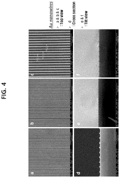
Technical Solution: Developed pioneering microtransfer printing technology using elastomeric stamps to transfer nanostructures from donor substrates to receiver substrates with high precision and yield. Their approach utilizes kinetically controlled adhesion mechanisms where the printing speed and contact pressure determine selective transfer. The technology enables deterministic assembly of heterogeneous nanostructures including quantum dots, nanowires, and 2D materials onto flexible and rigid substrates. They have demonstrated successful transfer of III-V semiconductor nanostructures for high-performance electronics and photonics applications with positioning accuracy below 1 micrometer.
Strengths: Pioneer in the field with extensive patent portfolio and proven scalability. Weaknesses: Limited to certain material systems and requires careful optimization of stamp properties.
Core Patents in Nanostructure Transfer Technologies
Apparatus and methods for micro-transfer printing
PatentWO2016012409A2
Innovation
- The use of high acceleration during the pick process, plasma treatment for improved bonding, and design features such as multi-tiered posts and anti-sag posts on the transfer device to enhance adhesion and prevent unwanted material pickup, along with heat-assisted printing and polymer encapsulation to facilitate printing on non-native substrates with topographic features.


Method of printing nanostructure
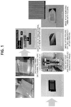
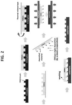
PatentPendingUS20240103362A1
Innovation
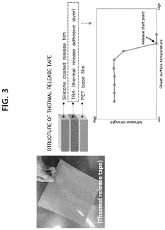
- A method involving a template substrate with a formed pattern, a polymer thin film coated with a thermal release tape, and functional material deposition on a replica pattern, followed by heat and pressure application to weaken adhesive forces and facilitate easy, large-scale printing of nanostructures on various substrates.
Manufacturing Standards for Nanostructure Processes
The establishment of robust manufacturing standards for nanostructure processes utilizing microtransfer printing represents a critical foundation for industrial scalability and quality assurance. Current standardization efforts focus on defining precise parameters for substrate preparation, donor wafer specifications, and transfer medium characteristics that ensure consistent nanostructure placement and integrity.
Key manufacturing standards encompass dimensional tolerances for nanostructures, typically requiring sub-10 nanometer precision in feature definition and positioning accuracy within ±50 nanometers for most applications. These specifications directly impact device performance in applications ranging from quantum dots in display technologies to nanoscale sensors in biomedical devices.
Process control standards mandate comprehensive monitoring of environmental conditions, including temperature stability within ±0.5°C, humidity control below 45% relative humidity, and particulate contamination levels not exceeding Class 10 cleanroom specifications. These parameters are essential for maintaining the delicate interface interactions that govern successful microtransfer printing operations.
Quality assurance protocols require multi-stage inspection procedures, incorporating atomic force microscopy for surface topology verification, scanning electron microscopy for structural integrity assessment, and optical characterization for functional validation. Statistical process control methods must demonstrate transfer yield rates exceeding 95% for commercial viability.
Standardized material specifications define acceptable donor substrate materials, including gallium arsenide, silicon, and specialized polymer carriers, each with specific surface energy requirements and thermal expansion coefficients. Transfer medium formulations must meet viscosity standards between 10-100 cP and maintain chemical stability under processing conditions.
Documentation standards require comprehensive traceability protocols, encompassing batch tracking, process parameter logging, and defect classification systems. These standards facilitate continuous improvement initiatives and enable rapid identification of process deviations that could compromise nanostructure quality or transfer efficiency in high-volume manufacturing environments.
Quality Control in Microtransfer Printing Applications
Quality control in microtransfer printing applications represents a critical aspect of ensuring reliable and reproducible nanostructure fabrication. The precision required for successful transfer of nanoscale features demands sophisticated monitoring and control mechanisms throughout the entire printing process. Effective quality control encompasses multiple stages, from substrate preparation and stamp characterization to post-transfer inspection and validation.
Real-time monitoring systems play a pivotal role in maintaining process consistency. Advanced optical inspection techniques, including high-resolution microscopy and interferometry, enable continuous assessment of stamp-substrate contact uniformity and transfer completeness. These systems can detect defects such as incomplete transfers, stamp deformation, or contamination particles that could compromise the final nanostructure quality. Integration of machine learning algorithms with inspection systems allows for predictive quality control, identifying potential issues before they manifest as defects.
Statistical process control methods are essential for maintaining long-term printing stability. Key performance indicators include transfer yield, dimensional accuracy, and defect density across printed arrays. Control charts and process capability studies help establish acceptable variation limits and trigger corrective actions when processes drift outside specification boundaries. Regular calibration of printing parameters, such as contact pressure, temperature, and dwell time, ensures consistent performance across production runs.
Metrology and characterization protocols form the backbone of quality assurance in microtransfer printing. Atomic force microscopy and scanning electron microscopy provide detailed assessment of transferred nanostructure fidelity, including feature dimensions, sidewall profiles, and surface roughness. Electrical testing methods validate functional performance of printed electronic devices, while optical characterization techniques assess photonic nanostructures.
Contamination control represents another crucial quality aspect, requiring cleanroom environments and rigorous material handling procedures. Stamp cleaning protocols, substrate surface preparation, and environmental monitoring prevent particle contamination that could disrupt the transfer process. Documentation and traceability systems ensure that quality issues can be rapidly identified and corrected, maintaining the high standards necessary for successful nanostructure fabrication through microtransfer printing.
Unlock deeper insights with Patsnap Eureka Quick Research — get a full tech report to explore trends and direct your research. Try now!
Generate Your Research Report Instantly with AI Agent
Supercharge your innovation with Patsnap Eureka AI Agent Platform!