

How to Maximize Microtransfer Printing Efficiency
APR 23, 20269 MIN READ
Generate Your Research Report Instantly with AI Agent
Patsnap Eureka helps you evaluate technical feasibility & market potential.
Microtransfer Printing Technology Background and Objectives
Microtransfer printing emerged as a revolutionary manufacturing technique in the early 2000s, initially developed to address the limitations of traditional semiconductor fabrication processes. This technology enables the precise transfer of microscale materials, components, or structures from a donor substrate to a receiver substrate using elastomeric stamps. The evolution from conventional photolithography-based methods to microtransfer printing represents a paradigm shift toward more flexible, cost-effective, and scalable manufacturing approaches.
The fundamental principle underlying microtransfer printing involves the controlled adhesion and release of materials through mechanical contact and separation processes. Early implementations focused primarily on transferring inorganic semiconductor materials, but the technology has since expanded to encompass organic materials, quantum dots, nanowires, and complex heterostructures. This versatility has positioned microtransfer printing as a critical enabling technology for next-generation electronic devices, displays, and photonic systems.
Current technological objectives center on achieving unprecedented levels of transfer efficiency while maintaining precise spatial control and material integrity. The primary goal involves maximizing the percentage of successfully transferred elements per printing cycle, which directly impacts manufacturing throughput and economic viability. Secondary objectives include minimizing defect rates, reducing material waste, and enabling high-resolution patterning capabilities across large substrate areas.
The technology aims to bridge the gap between laboratory-scale demonstrations and industrial-scale production by addressing fundamental challenges in adhesion control, stamp design optimization, and process parameter standardization. Advanced objectives encompass the development of multi-material printing capabilities, three-dimensional assembly techniques, and integration with existing semiconductor manufacturing infrastructure.
Strategic technological targets include achieving transfer efficiencies exceeding 99.9% for critical applications, enabling sub-micron registration accuracy, and establishing reliable processes for heterogeneous integration of dissimilar materials. These objectives drive ongoing research efforts in surface chemistry modification, stamp material engineering, and automated process control systems, ultimately positioning microtransfer printing as a cornerstone technology for future electronics manufacturing paradigms.
Market Demand for High-Efficiency Microtransfer Printing
The market demand for high-efficiency microtransfer printing technology is experiencing unprecedented growth, driven by the rapid expansion of advanced display technologies and next-generation semiconductor applications. The global shift toward micro-LED displays, augmented reality devices, and flexible electronics has created substantial market opportunities for companies that can deliver superior microtransfer printing solutions. Consumer electronics manufacturers are increasingly seeking production methods that can achieve higher throughput while maintaining exceptional precision and yield rates.
Display technology represents the largest market segment driving demand for enhanced microtransfer printing efficiency. Major display manufacturers are transitioning from traditional OLED technologies to micro-LED arrays for premium applications, including high-end smartphones, smartwatches, and large-format displays. The stringent requirements for pixel density, color uniformity, and manufacturing scalability have intensified the need for microtransfer printing processes that can handle millions of microscopic components with minimal defect rates.
The semiconductor industry constitutes another significant demand driver, particularly in the development of advanced packaging solutions and heterogeneous integration applications. As chip manufacturers pursue more complex multi-die configurations and 3D packaging architectures, the ability to efficiently transfer and place microscopic components with nanometer-level accuracy has become critical for maintaining competitive advantage and meeting performance specifications.
Emerging applications in biomedical devices and sensors are creating additional market opportunities for high-efficiency microtransfer printing technologies. The growing demand for miniaturized medical implants, lab-on-chip devices, and wearable health monitoring systems requires manufacturing processes capable of handling diverse materials and achieving precise placement of functional components at microscopic scales.
Market pressures are intensifying as production volumes increase and cost reduction targets become more aggressive. Manufacturers are actively seeking microtransfer printing solutions that can deliver higher throughput rates, reduced material waste, and improved process reliability. The economic viability of next-generation products increasingly depends on achieving manufacturing efficiencies that were previously considered technically unfeasible.
Geographic market dynamics show concentrated demand in Asia-Pacific regions, where major electronics manufacturers are establishing advanced production facilities. However, growing demand is also emerging in North America and Europe as companies invest in domestic manufacturing capabilities for strategic technologies and supply chain resilience.
Current Status and Challenges in Microtransfer Printing
Microtransfer printing has emerged as a critical technology for advanced manufacturing applications, particularly in the semiconductor, display, and biomedical device industries. Currently, the technology demonstrates significant capabilities in transferring microscale materials with precision, yet several fundamental challenges continue to limit its widespread adoption and optimal performance.
The present state of microtransfer printing technology reveals substantial variations in transfer efficiency across different material systems and substrate combinations. Silicon-based micro-devices achieve transfer rates of 85-95% under optimal conditions, while organic semiconductor materials typically exhibit lower success rates of 60-80%. These disparities stem from fundamental differences in material properties, surface energies, and adhesion characteristics that govern the transfer process.
Interface control represents one of the most significant technical barriers in current implementations. The delicate balance between stamp adhesion during pickup and release phases requires precise control of surface treatments, temperature, and contact pressure. Existing elastomeric stamp materials, primarily polydimethylsiloxane (PDMS) derivatives, suffer from limited durability and inconsistent surface properties after repeated use cycles, leading to gradual degradation in transfer fidelity.
Alignment accuracy poses another critical challenge, particularly for applications requiring sub-micron positioning precision. Current systems struggle to maintain consistent registration across large substrate areas, with thermal expansion, mechanical vibrations, and stamp deformation contributing to cumulative positioning errors. The lack of real-time feedback mechanisms further compounds these alignment difficulties.
Process scalability remains constrained by throughput limitations inherent in current serial transfer approaches. While laboratory demonstrations show promising results for small-scale transfers, industrial-scale production demands significantly higher processing speeds and yield consistency. The sequential nature of most existing processes creates bottlenecks that limit commercial viability for high-volume manufacturing applications.
Material compatibility issues continue to restrict the range of transferable components. Different material systems require customized process parameters, stamp surface modifications, and environmental controls, making it challenging to develop universal processing protocols. This limitation particularly affects multi-material device integration and complex heterogeneous system assembly.
Geographically, microtransfer printing development concentrates primarily in advanced manufacturing regions, with significant research activities in North America, East Asia, and Europe. However, the technology transfer from research institutions to industrial implementation remains uneven, creating gaps between demonstrated capabilities and commercially available solutions.
Current Solutions for Microtransfer Printing Efficiency
01 Stamp material and surface modification for improved transfer efficiency
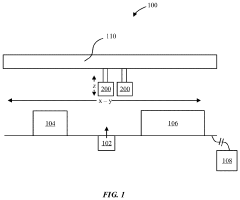
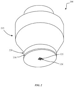
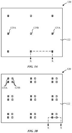
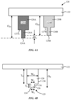
The efficiency of microtransfer printing can be enhanced by optimizing the stamp material properties and surface characteristics. This includes selecting appropriate elastomeric materials with suitable adhesion properties, modifying surface energy through treatments, and controlling surface roughness. The stamp material's mechanical properties such as elasticity and flexibility play crucial roles in achieving conformal contact with the substrate and facilitating clean release of printed materials.- Stamp design and material optimization for transfer printing: The efficiency of microtransfer printing can be significantly improved through optimized stamp design and material selection. Key factors include the surface energy, elasticity, and microstructure of the stamp material. Polydimethylsiloxane (PDMS) and other elastomeric materials with controlled surface properties enable better contact and release characteristics. The stamp geometry, including feature size, pattern density, and surface texture, directly affects the pick-up and transfer yield of micro/nano materials.
- Interface adhesion control and surface treatment methods: Controlling interfacial adhesion between the stamp, ink material, and receiving substrate is critical for high-efficiency transfer. Surface treatment techniques such as plasma treatment, chemical modification, and self-assembled monolayers can modulate adhesion forces. The balance between pick-up adhesion and release adhesion determines transfer success rates. Dynamic control of adhesion through external stimuli like temperature, pressure, or chemical environment enables selective and efficient transfer of materials.
- Process parameter optimization and printing conditions: Transfer printing efficiency is highly dependent on process parameters including contact pressure, contact time, separation speed, and environmental conditions. Optimizing these parameters for specific material systems improves yield and uniformity. Temperature control during the transfer process affects material properties and adhesion behavior. Automated control systems and real-time monitoring enable consistent high-efficiency transfer across large areas and multiple cycles.
- Ink material properties and formulation strategies: The properties of the ink material being transferred significantly impact printing efficiency. Material characteristics such as thickness, mechanical properties, surface chemistry, and structural integrity affect both pick-up and transfer processes. Formulation strategies including the use of sacrificial layers, adhesion promoters, and material composites can enhance transfer rates. Pre-patterning and material preparation techniques ensure consistent material properties for reliable high-efficiency transfer.
- Equipment design and automation for high-throughput transfer: Advanced equipment design incorporating precision alignment systems, automated handling mechanisms, and parallel processing capabilities enables high-throughput microtransfer printing. Multi-stamp configurations and roll-to-roll processing systems increase production efficiency. Integration of vision systems and feedback control ensures accurate placement and high yield. Modular equipment designs allow flexibility for different material systems and application requirements while maintaining high transfer efficiency.
02 Ink formulation and rheological properties optimization
Transfer efficiency can be significantly improved through careful formulation of the ink materials. This involves controlling viscosity, surface tension, and adhesion characteristics of the ink to ensure proper transfer from the stamp to the substrate. The ink composition may include additives and modifiers that enhance wetting behavior and promote complete transfer while preventing residue on the stamp surface.Expand Specific Solutions03 Process parameter control and printing conditions
Optimizing process parameters such as contact pressure, contact time, temperature, and separation speed is critical for achieving high transfer efficiency. Precise control of these parameters ensures adequate adhesion during contact and clean release during separation. Environmental conditions including humidity and temperature control also contribute to consistent and efficient transfer results.Expand Specific Solutions04 Substrate surface preparation and treatment
The substrate surface condition significantly affects transfer efficiency. Surface preparation techniques including cleaning, plasma treatment, chemical modification, and application of adhesion promotion layers can enhance the bonding between transferred materials and substrates. Controlling substrate surface energy and roughness ensures better acceptance of printed materials and reduces defects.Expand Specific Solutions05 Equipment design and alignment systems
Advanced equipment design incorporating precise alignment mechanisms, uniform pressure distribution systems, and automated control features can substantially improve transfer efficiency. This includes development of specialized printing apparatus with enhanced positioning accuracy, real-time monitoring capabilities, and feedback control systems that ensure consistent transfer quality across large areas and multiple printing cycles.Expand Specific Solutions
Key Players in Microtransfer Printing Industry
The microtransfer printing technology landscape is in a growth phase, transitioning from research-driven development to commercial applications across multiple industries. The market demonstrates significant potential with diverse applications spanning display manufacturing, semiconductor integration, and advanced materials processing. Technology maturity varies considerably among market participants, with specialized companies like X Display Co. Technology Ltd. leading in dedicated microtransfer printing solutions, while established giants including Canon, Xerox, and BOE Technology Group leverage their manufacturing expertise to integrate these capabilities. Academic institutions such as Zhejiang University and Ghent University continue advancing fundamental research, while industrial players like Sharp, LG Chem, and Apple drive practical implementation. The competitive landscape shows a hybrid ecosystem where traditional printing companies, semiconductor manufacturers, and display technology firms converge, indicating the technology's cross-industry relevance and commercial viability.
X Display Co. Technology Ltd.
Technical Solution: X-Display has developed advanced microtransfer printing technology specifically for micro-LED displays, utilizing elastomeric stamps with optimized surface properties to achieve high-yield transfer of microscale LEDs. Their approach focuses on controlling adhesion forces through surface engineering and precise temperature control during the pick-and-place process. The company has demonstrated transfer efficiencies exceeding 99.9% for LED chips smaller than 10 micrometers, employing selective release mechanisms that minimize damage to both the donor substrate and receiving surface.
Strengths: Industry-leading transfer yield rates, specialized micro-LED focus, proven scalability for mass production. Weaknesses: Limited application beyond display technologies, high equipment costs, dependency on specific substrate materials.
BOE Technology Group Co., Ltd.
Technical Solution: BOE has implemented a comprehensive microtransfer printing solution combining laser-assisted selective transfer with advanced stamp materials for large-area display manufacturing. Their technology incorporates real-time monitoring systems and adaptive process control to maintain consistent transfer quality across different substrate sizes. The company utilizes proprietary adhesive release layers and optimized thermal cycling to achieve reliable transfer of components ranging from 5-50 micrometers, with particular emphasis on maintaining electrical connectivity during the transfer process.
Strengths: Large-scale manufacturing capability, integrated process monitoring, cost-effective for high-volume production. Weaknesses: Lower precision compared to specialized equipment, limited flexibility for research applications, requires significant capital investment.
Core Technologies for Maximizing Transfer Efficiency
Single-Pick-Multiple-Print Micro LED Mass Transfer with Elastomer Stamp
PatentPendingUS20240234181A1
Innovation
- The use of conformable transfer devices with arrays of transfer heads of different lengths, combined with an adhesive film on the receiving substrate, allows for high-density transfer of micro devices by picking up multiple devices simultaneously and placing them sequentially without contacting the adhesive film, thereby reducing cycle time and improving efficiency.
Multi-layer tethers for micro-transfer printing
PatentActiveUS20210020491A1
Innovation
- A micro-device structure featuring a source substrate with sacrificial portions and anchors, laterally attached by a multi-layer tether comprising different materials and thicknesses, such as silicon dioxide and silicon nitride, to maintain precise positioning and facilitate efficient transfer.


Manufacturing Standards for Microtransfer Processes
Manufacturing standards for microtransfer processes represent a critical framework that governs the precision, repeatability, and quality control aspects of microtransfer printing operations. These standards encompass dimensional tolerances, material specifications, environmental controls, and process validation protocols that directly impact printing efficiency outcomes.
The establishment of standardized substrate preparation protocols forms the foundation of efficient microtransfer operations. Surface roughness parameters must be maintained within nanometer-scale tolerances, typically requiring Ra values below 5 nanometers for optimal adhesion characteristics. Cleanliness standards mandate particulate contamination levels not exceeding Class 100 cleanroom specifications, as microscopic debris can significantly compromise transfer yield rates.
Temperature and humidity control standards are essential for maintaining consistent material properties throughout the printing process. Operating temperatures should be regulated within ±0.5°C variations, while relative humidity must remain stable between 45-55% to prevent thermal expansion mismatches and moisture-induced adhesion variations that can reduce transfer efficiency.
Alignment accuracy standards define the precision requirements for substrate positioning and pattern registration. Current industry benchmarks specify alignment tolerances within ±1 micrometer for high-efficiency applications, necessitating advanced metrology systems and real-time feedback control mechanisms to maintain these stringent requirements consistently.
Material handling and storage protocols establish guidelines for maintaining ink and substrate integrity prior to processing. These standards include specific packaging requirements, shelf-life limitations, and pre-process conditioning procedures that ensure optimal material performance during transfer operations.
Quality assurance standards incorporate statistical process control methodologies to monitor key performance indicators such as transfer yield, pattern fidelity, and defect density. These metrics enable continuous process optimization and early detection of efficiency degradation, supporting sustained high-performance manufacturing operations.
Calibration and maintenance standards ensure equipment performance consistency over extended operational periods. Regular calibration schedules for critical components, preventive maintenance protocols, and performance verification procedures are essential elements that maintain the precision required for maximum transfer efficiency achievement.
Cost-Benefit Analysis of High-Efficiency Systems
The economic evaluation of high-efficiency microtransfer printing systems reveals a complex landscape of initial investments versus long-term operational benefits. Advanced systems typically require capital expenditures ranging from $2-5 million for industrial-scale equipment, significantly higher than conventional printing technologies. However, the enhanced throughput capabilities and reduced material waste create compelling value propositions for high-volume manufacturing environments.
Operational cost analysis demonstrates substantial advantages in material utilization efficiency. High-efficiency systems achieve transfer yields exceeding 99.5%, compared to 85-90% for standard equipment, resulting in material cost savings of 10-15% annually. The precision control mechanisms reduce substrate waste and minimize rework requirements, contributing to overall cost reduction. Energy consumption patterns show mixed results, with sophisticated control systems consuming 20-30% more power during operation, but achieving faster processing times that offset the increased energy costs.
Labor cost implications present favorable outcomes for high-efficiency implementations. Automated handling and real-time monitoring capabilities reduce operator intervention requirements by approximately 40%, translating to significant labor cost savings in high-volume production scenarios. The enhanced process stability minimizes downtime and maintenance interventions, further improving operational efficiency metrics.
Return on investment calculations indicate break-even points typically occurring within 18-24 months for facilities processing over 10,000 substrates monthly. The economic benefits become more pronounced at higher production volumes, where the fixed costs of advanced equipment are amortized across larger output quantities. Quality improvements associated with high-efficiency systems also contribute to reduced customer returns and enhanced market positioning.
Risk assessment considerations include technology obsolescence concerns and the need for specialized technical support, which may increase long-term operational costs. However, the competitive advantages gained through superior product quality and manufacturing efficiency generally outweigh these potential drawbacks in strategic market positioning.
Unlock deeper insights with Patsnap Eureka Quick Research — get a full tech report to explore trends and direct your research. Try now!
Generate Your Research Report Instantly with AI Agent
Supercharge your innovation with Patsnap Eureka AI Agent Platform!