How to Lower Semiconductor Wafer Bending during Etching
MAR 31, 20268 MIN READ
Generate Your Research Report Instantly with AI Agent
Patsnap Eureka helps you evaluate technical feasibility & market potential.
Semiconductor Wafer Etching Background and Objectives
Semiconductor wafer etching represents a fundamental process in modern microelectronics manufacturing, serving as the cornerstone for creating intricate patterns and structures on silicon substrates. This critical fabrication step involves the selective removal of material from wafer surfaces through chemical or physical means, enabling the formation of transistors, interconnects, and other essential components that define contemporary integrated circuits.
The evolution of semiconductor manufacturing has witnessed remarkable progress from early micron-scale features to today's advanced nodes operating at 3nm and below. Throughout this technological journey, etching processes have continuously adapted to meet increasingly stringent requirements for precision, uniformity, and dimensional control. However, as device geometries shrink and wafer sizes expand to 300mm and beyond, new challenges have emerged that threaten manufacturing yield and product reliability.
Wafer bending during etching has become a particularly pressing concern in advanced semiconductor fabrication. This phenomenon occurs when non-uniform stress distributions develop across the wafer surface during material removal processes, leading to mechanical deformation that can compromise device performance and manufacturing efficiency. The issue has intensified with the adoption of complex multi-layer structures, high-aspect-ratio features, and aggressive etching chemistries required for cutting-edge technology nodes.
The primary objective of addressing wafer bending challenges centers on maintaining dimensional stability throughout the etching process while preserving critical device specifications. This involves developing comprehensive understanding of stress generation mechanisms, implementing real-time monitoring systems, and establishing process control strategies that minimize mechanical distortion. Success in this endeavor directly impacts yield optimization, device reliability, and overall manufacturing cost-effectiveness.
Contemporary research efforts focus on achieving sub-nanometer level control over wafer flatness during etching operations. The target encompasses not only immediate process improvements but also long-term scalability to support future technology roadmaps. These objectives align with industry demands for enhanced manufacturing precision, reduced defect rates, and improved process robustness across diverse product portfolios and application domains.
Market Demand for High-Quality Wafer Processing
The semiconductor industry faces unprecedented demand for high-quality wafer processing as device miniaturization continues to push technological boundaries. Advanced semiconductor nodes below 7nm require exceptional dimensional accuracy and surface quality, making wafer flatness a critical parameter throughout the manufacturing process. Even minor wafer bending during etching can result in significant yield losses and performance degradation in final devices.
Market drivers for superior wafer processing quality stem from multiple sectors experiencing rapid growth. The artificial intelligence and machine learning boom has created substantial demand for high-performance computing chips that require precise geometries and minimal defects. Data centers worldwide are expanding their capacity to handle increasing computational loads, driving demand for processors manufactured with the highest quality standards.
The automotive industry's transition toward electric vehicles and autonomous driving systems has generated new requirements for semiconductor reliability and performance. These applications demand chips that can operate under extreme conditions while maintaining consistent performance, making wafer quality during processing absolutely critical. Any bending-induced defects during etching can compromise the long-term reliability essential for automotive applications.
Consumer electronics continue to drive volume demand for high-quality semiconductor processing. Smartphones, tablets, and wearable devices require increasingly sophisticated chips packed into smaller form factors. The competitive nature of consumer markets means that manufacturers cannot afford yield losses or performance variations caused by wafer processing issues.
Industrial Internet of Things applications represent an emerging market segment with stringent quality requirements. These devices often operate in harsh environments for extended periods, necessitating semiconductors manufactured with exceptional precision and consistency. Wafer bending during etching can introduce stress patterns that compromise device reliability in these demanding applications.
The economic impact of wafer processing quality extends beyond immediate manufacturing costs. Poor wafer flatness during etching can reduce overall fab utilization efficiency, increase rework requirements, and delay time-to-market for new products. As semiconductor manufacturing costs continue to rise with each technology node, maintaining optimal wafer processing conditions becomes increasingly critical for economic viability.
Current Wafer Bending Issues and Technical Challenges
Wafer bending during semiconductor etching processes represents one of the most critical manufacturing challenges in modern chip fabrication. This phenomenon occurs when non-uniform stress distributions across the wafer surface cause mechanical deformation, leading to thickness variations and compromised device performance. The issue becomes increasingly severe as wafer sizes expand to 300mm and beyond, where even minimal stress gradients can result in significant geometric distortions.
The primary technical challenge stems from thermal gradients generated during plasma etching processes. As reactive ions bombard the wafer surface, localized heating creates temperature differentials that induce thermal stress. These stress concentrations are particularly pronounced at the wafer edges, where heat dissipation characteristics differ significantly from the central regions. The resulting thermal expansion mismatch between different wafer areas directly contributes to bending deformation.
Chemical etching processes introduce additional complexity through non-uniform material removal rates across the wafer surface. Variations in etchant concentration, flow dynamics, and surface chemistry create localized stress patterns that accumulate throughout the etching cycle. This chemical-mechanical coupling effect is especially problematic in deep silicon etching applications, where high aspect ratio structures amplify stress concentrations.
Process-induced stress represents another fundamental challenge category. Ion bombardment energy, plasma density variations, and chamber pressure fluctuations all contribute to non-uniform stress distributions. The interaction between these process parameters creates complex stress fields that are difficult to predict and control using conventional process monitoring techniques.
Equipment-related factors further compound wafer bending issues. Chuck design limitations, vacuum distribution irregularities, and electrostatic clamping force variations can introduce mechanical stress patterns that persist throughout the etching process. Temperature control system inadequacies often fail to maintain uniform thermal conditions, particularly during high-power plasma operations.
Material property variations within the wafer substrate itself present inherent challenges. Crystal orientation differences, dopant concentration gradients, and pre-existing stress from upstream processing steps create baseline stress conditions that etching processes can amplify. These material-related factors are particularly challenging because they vary between wafer lots and cannot be easily controlled through process parameter adjustments.
The measurement and characterization of wafer bending present additional technical hurdles. Real-time monitoring systems must operate in harsh plasma environments while maintaining sufficient sensitivity to detect subtle deformation patterns. Current metrology approaches often lack the spatial resolution and temporal response needed for effective process control feedback.
Existing Solutions for Wafer Stress Control
01 Wafer chuck and holding mechanisms to prevent bending
Specialized wafer chucks and holding mechanisms are designed to securely hold semiconductor wafers during processing while minimizing stress and preventing bending. These mechanisms utilize vacuum suction, mechanical clamping, or electrostatic forces to maintain wafer flatness. The design considerations include uniform pressure distribution, temperature control, and material selection to reduce thermal expansion mismatch that could cause wafer deformation.- Wafer chuck and holding mechanisms to prevent bending: Specialized wafer chucks and holding mechanisms are designed to securely hold semiconductor wafers during processing while minimizing stress and preventing bending. These mechanisms utilize vacuum suction, mechanical clamping, or electrostatic forces to maintain wafer flatness. The design considerations include uniform pressure distribution, temperature control, and material selection to reduce thermal expansion mismatch that could cause wafer deformation.
- Wafer support structures and carriers: Support structures and carriers are developed to transport and process wafers while maintaining their structural integrity. These include wafer boats, cassettes, and frames with specific geometric designs that provide support at optimal contact points to distribute weight evenly and prevent sagging or warping. The materials used in these structures are selected for their thermal stability and low particle generation properties.
- Stress relief and thermal management techniques: Methods for managing thermal stress and mechanical stress during wafer processing are implemented to reduce bending. These techniques include controlled heating and cooling rates, annealing processes, and the use of buffer layers or stress-compensating films. Temperature uniformity across the wafer surface is maintained through advanced heating systems and real-time monitoring to prevent thermal gradients that lead to warping.
- Wafer flatness measurement and correction systems: Measurement systems and correction mechanisms are employed to detect and compensate for wafer bending. These include optical sensors, laser interferometry, and capacitive sensors that measure wafer surface topology and deviation from flatness. Based on measurement data, active correction systems can apply controlled pressure or adjust processing parameters to restore wafer flatness during manufacturing operations.
- Wafer thinning and backside processing methods: Techniques for wafer thinning and backside processing are optimized to minimize induced stress and bending. These methods include grinding, polishing, and chemical mechanical planarization processes with controlled removal rates and pressure application. Temporary bonding and support wafer technologies are utilized during thinning operations to provide mechanical support and prevent breakage or excessive bending of ultra-thin wafers.
02 Wafer support structures and carriers
Support structures and carriers are developed to transport and process wafers while maintaining their structural integrity. These include specially designed trays, cassettes, and frames that provide adequate support across the wafer surface to prevent sagging or bending during handling and processing. The support structures often feature optimized contact point distributions and materials with matched thermal properties to minimize stress-induced deformation.Expand Specific Solutions03 Thermal stress management during processing
Methods and apparatus for managing thermal stress during semiconductor wafer processing are employed to prevent bending caused by temperature gradients. These approaches include controlled heating and cooling rates, uniform temperature distribution systems, and thermal compensation techniques. The solutions address thermal expansion coefficient differences between wafer materials and processing equipment, which can lead to warpage and bending during high-temperature processes.Expand Specific Solutions04 Wafer flattening and correction devices
Devices and methods for detecting and correcting wafer bending are utilized to restore flatness to deformed wafers. These include mechanical flattening systems, stress relief treatments, and real-time monitoring equipment that can measure wafer bow and warp. Correction techniques may involve applying controlled pressure, thermal treatment, or laser-based processes to redistribute internal stresses and restore the wafer to its original flat state.Expand Specific Solutions05 Wafer thinning and grinding processes to reduce bending
Optimized wafer thinning and grinding processes are developed to reduce thickness while minimizing the introduction of mechanical stress that causes bending. These processes include multi-stage grinding with progressively finer abrasives, stress-relief grinding patterns, and post-grinding treatments. The methods focus on achieving uniform material removal, controlling subsurface damage, and managing residual stress to prevent wafer warpage during and after the thinning process.Expand Specific Solutions
Key Players in Semiconductor Equipment Industry
The semiconductor wafer bending mitigation technology represents a mature yet evolving market segment within the broader semiconductor manufacturing ecosystem. The industry is in an advanced development stage, driven by increasing demands for thinner wafers and more precise manufacturing processes. Market leaders include established equipment manufacturers like Applied Materials, Lam Research, and Tokyo Electron, who provide comprehensive etching solutions, alongside major foundries such as Taiwan Semiconductor Manufacturing Company and Samsung Electronics that implement these technologies at scale. Silicon wafer suppliers like SUMCO Corp. and Siltronic AG contribute specialized substrate solutions, while companies like Hitachi High-Tech America and Electro Scientific Industries offer precision measurement and control systems. The technology maturity varies across applications, with basic stress management techniques well-established, while advanced real-time compensation methods remain under active development, particularly for next-generation node requirements.
Lam Research Corp.
Technical Solution: Lam Research has developed advanced plasma etching systems with real-time wafer stress monitoring and compensation technologies. Their Kiyo and Flex series etchers incorporate sophisticated chuck temperature control systems that maintain uniform thermal distribution across the wafer surface during etching processes. The company utilizes multi-zone electrostatic chucks with independent temperature control zones to minimize thermal gradients that cause wafer bending. Additionally, their proprietary plasma confinement rings and edge exclusion technologies help reduce non-uniform etching rates at wafer edges, which is a primary contributor to stress-induced bending. The systems also feature advanced endpoint detection algorithms that prevent over-etching, thereby reducing cumulative stress buildup in the wafer structure.
Strengths: Industry-leading plasma control technology and comprehensive thermal management systems. Weaknesses: High equipment costs and complex maintenance requirements for multi-zone control systems.
Applied Materials, Inc.
Technical Solution: Applied Materials employs their Centura platform with innovative wafer clamping and support mechanisms designed to minimize mechanical stress during etching. Their approach includes the use of backside gas cooling systems that provide uniform temperature distribution while maintaining precise wafer flatness through controlled pressure differentials. The company has developed proprietary etch chamber designs with optimized gas flow patterns that ensure uniform plasma density distribution, reducing localized stress concentrations. Their Producer series systems incorporate real-time wafer bow measurement capabilities using laser interferometry, allowing for dynamic process adjustments to compensate for developing stress patterns. Advanced process recipes include multi-step etching sequences with intermediate stress relief steps to prevent cumulative bending effects.
Strengths: Comprehensive process control and real-time monitoring capabilities with proven high-volume manufacturing reliability. Weaknesses: Limited flexibility in retrofitting existing equipment and high initial capital investment requirements.
Core Innovations in Wafer Bending Prevention
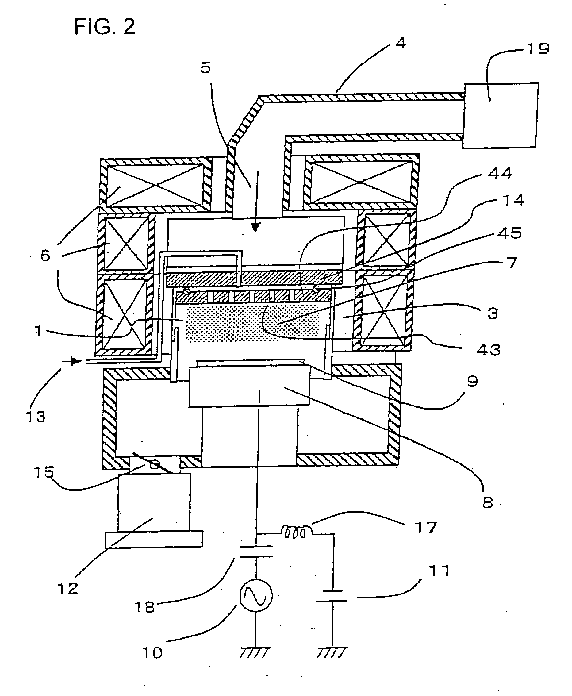
Method of manufacturing a wafer
PatentInactiveUS6878630B2
Innovation
- The method optimizes the caustic etch process by using a diluted KOH etchant and controls the wafer back side polishing process to minimize the step between the central and edge portions, ensuring uniform surface roughness and preventing sliding phenomena during etching, while maintaining adequate chucking voltage.


Apparatus and method for processing wafer
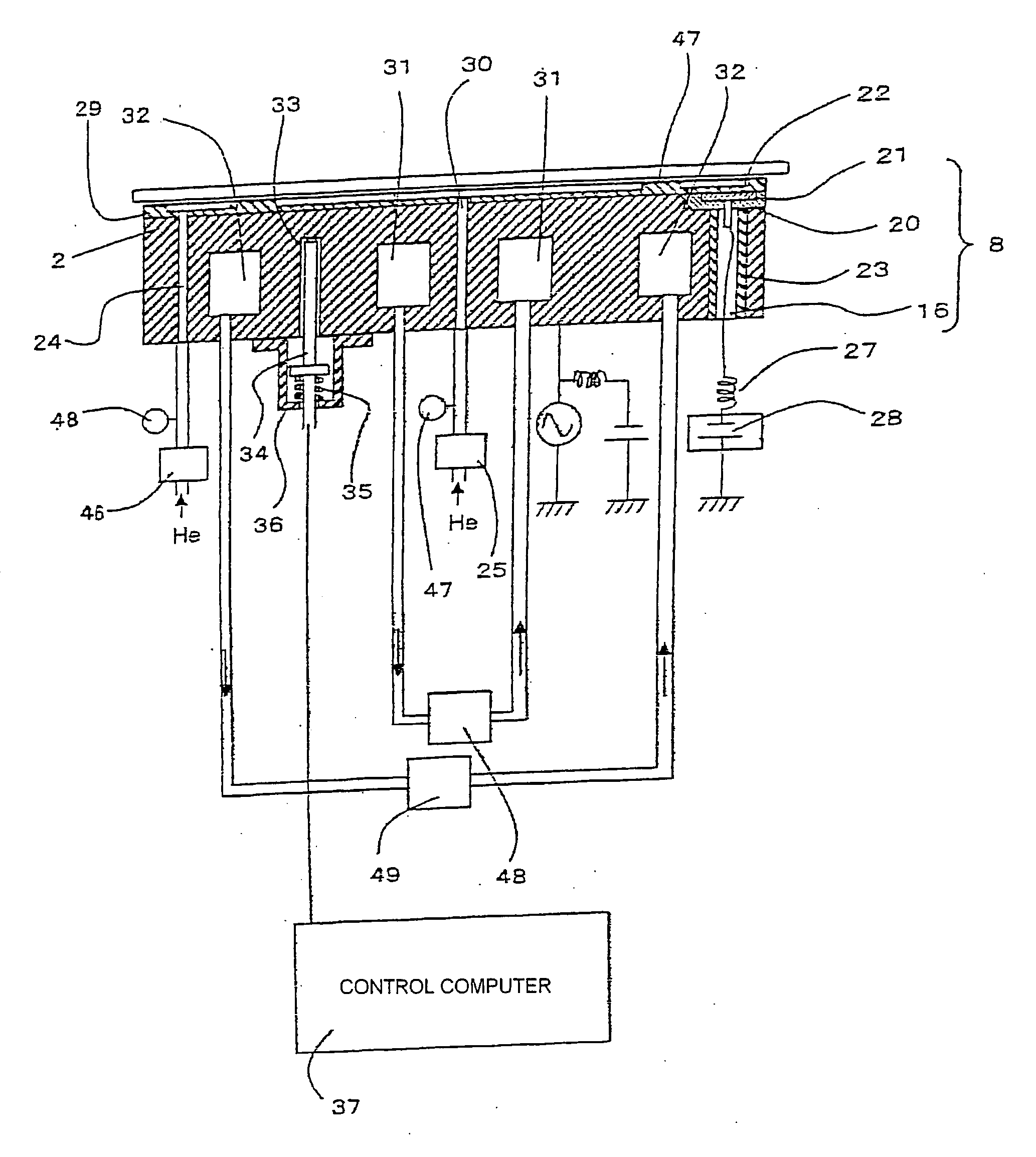
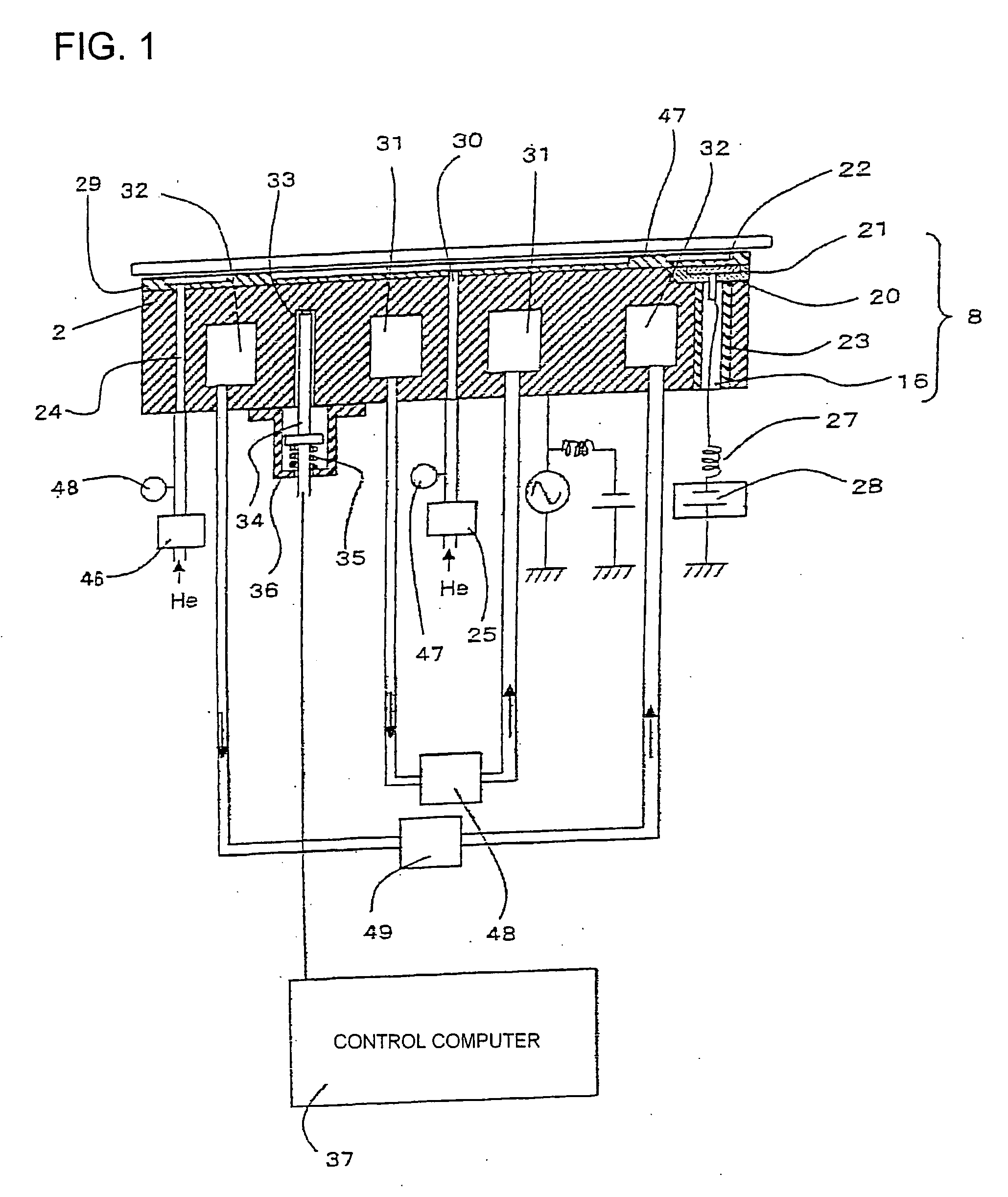
PatentInactiveUS20060191482A1
Innovation
- A wafer processing apparatus and method that regulate the semiconductor wafer's temperature using separate temperature regulating agent circuits, cooling gas pressure, and heater power, with a control computer determining optimal temperature conditions for uniform CD distribution based on measured data and relationship equations.

Process Control Standards for Wafer Manufacturing
Process control standards for wafer manufacturing represent a critical framework for maintaining dimensional stability and minimizing wafer bending during etching operations. These standards encompass comprehensive measurement protocols, tolerance specifications, and real-time monitoring systems that ensure consistent wafer geometry throughout the fabrication process.
The foundation of effective process control lies in establishing precise baseline measurements for wafer flatness, thickness uniformity, and stress distribution before etching begins. Industry standards such as SEMI M1 and M43 define acceptable limits for total thickness variation (TTV) and bow/warp measurements, typically requiring values below 1-2 micrometers for advanced semiconductor processes. These baseline parameters serve as reference points for subsequent process monitoring and adjustment.
Temperature control standards constitute another essential component, mandating uniform thermal distribution across the wafer surface during etching. Process specifications typically require temperature uniformity within ±2°C across the entire wafer, with gradual ramping rates not exceeding 5°C per minute to minimize thermal stress accumulation. Advanced process control systems integrate multiple temperature sensors and feedback loops to maintain these stringent requirements.
Chemical delivery and plasma uniformity standards ensure consistent etching rates across the wafer surface, preventing localized stress concentrations that contribute to bending. These standards specify precise flow rates, pressure tolerances, and gas composition requirements, with typical variations maintained within ±1% of target values. Real-time monitoring systems continuously track these parameters and implement automatic corrections when deviations occur.
Statistical process control (SPC) methodologies form the backbone of modern wafer manufacturing standards, employing control charts and capability indices to monitor process stability. These systems track key metrics such as etch rate uniformity, selectivity ratios, and post-etch wafer geometry measurements, triggering alerts when processes drift beyond established control limits. Implementation of these standards requires sophisticated data collection systems and automated feedback mechanisms that can respond to process variations within seconds.
Equipment Design Considerations for Wafer Flatness
Equipment design plays a critical role in maintaining wafer flatness during semiconductor etching processes. The fundamental approach involves creating uniform process conditions across the entire wafer surface while minimizing mechanical stress factors that contribute to wafer deformation. Modern etching equipment incorporates sophisticated chuck designs, precise temperature control systems, and optimized gas flow dynamics to achieve these objectives.
Chuck design represents the most crucial equipment consideration for wafer flatness control. Electrostatic chucks with optimized electrode patterns ensure uniform clamping force distribution across the wafer backside, preventing localized stress concentrations that lead to bending. Advanced chuck designs feature segmented electrodes that allow independent voltage control across different wafer regions, enabling real-time flatness adjustment during processing. The chuck surface finish and material selection also significantly impact thermal conductivity and mechanical coupling with the wafer.
Temperature uniformity across the wafer surface requires sophisticated thermal management systems within the equipment design. Multi-zone heating and cooling capabilities allow precise temperature control at different radial positions, compensating for non-uniform heat generation during etching. Advanced systems incorporate embedded temperature sensors and feedback control loops that continuously adjust heating power distribution to maintain isothermal conditions across the wafer surface.
Gas flow distribution systems must be engineered to provide uniform chemical species delivery and byproduct removal across the entire wafer area. Showerhead designs with optimized hole patterns and flow impedance ensure consistent gas residence time and reaction rates, preventing differential etching that contributes to stress-induced bending. Computational fluid dynamics modeling guides the optimization of gas injection and exhaust port configurations.
Plasma uniformity control represents another critical equipment design aspect. RF power delivery systems with multiple frequency capabilities and impedance matching networks enable precise plasma density control across the wafer surface. Magnetic field configurations and chamber geometry optimization help achieve uniform plasma characteristics, reducing spatial variations in ion bombardment energy and flux that contribute to non-uniform stress development during etching processes.
Unlock deeper insights with Patsnap Eureka Quick Research — get a full tech report to explore trends and direct your research. Try now!
Generate Your Research Report Instantly with AI Agent
Supercharge your innovation with Patsnap Eureka AI Agent Platform!