How To Mitigate Ion Contamination In Electrostatic Chuck Operations
MAY 14, 20269 MIN READ
Generate Your Research Report Instantly with AI Agent
PatSnap Eureka helps you evaluate technical feasibility & market potential.
Ion Contamination in ESC Technology Background and Objectives
Electrostatic chucks (ESCs) have emerged as critical components in semiconductor manufacturing processes, particularly in plasma-based etching and deposition systems. These devices utilize electrostatic forces to securely hold and position wafers during processing, eliminating the need for mechanical clamping mechanisms that could introduce contamination or damage. The technology has evolved significantly since its introduction in the 1980s, driven by the semiconductor industry's relentless pursuit of smaller feature sizes and higher device densities.
The fundamental principle of ESC operation involves applying a DC voltage between electrodes embedded within a dielectric material, creating an electrostatic attraction force that holds the wafer against the chuck surface. However, this electrostatic environment inherently creates conditions conducive to ion generation and accumulation, particularly when exposed to plasma environments commonly used in semiconductor fabrication processes.
Ion contamination in ESC operations represents a multifaceted challenge that directly impacts manufacturing yield, device reliability, and process consistency. The contamination manifests through various mechanisms including plasma-induced ion bombardment, charge accumulation on dielectric surfaces, and electrostatic discharge events. These phenomena can lead to wafer damage, non-uniform processing conditions, and degradation of the ESC itself over time.
The primary technical objectives for addressing ion contamination encompass several critical areas. First, minimizing ion generation through optimized ESC design and material selection represents a fundamental approach. This involves developing dielectric materials with superior electrical properties, implementing advanced electrode configurations, and establishing proper grounding schemes to control charge distribution.
Second, effective ion neutralization strategies must be developed to manage unavoidable ion accumulation. This includes implementing active charge dissipation systems, utilizing plasma-based neutralization techniques, and incorporating conductive pathways that safely redirect accumulated charges without compromising wafer processing integrity.
Third, real-time monitoring and control systems are essential for detecting and responding to ion contamination events. Advanced sensing technologies capable of measuring surface charge distribution, ion flux density, and electrostatic field variations enable proactive contamination management and process optimization.
The ultimate goal extends beyond mere contamination mitigation to achieving predictable, repeatable ESC performance that supports advanced semiconductor manufacturing requirements. This encompasses maintaining consistent clamping forces, ensuring uniform temperature distribution across the wafer surface, and preserving long-term ESC reliability under demanding operational conditions. Success in these objectives directly translates to improved manufacturing yields, reduced defect rates, and enhanced overall process capability in next-generation semiconductor fabrication facilities.
Market Demand for Clean ESC Operations in Semiconductor Manufacturing
The semiconductor manufacturing industry faces unprecedented pressure to maintain ultra-clean processing environments as device geometries continue to shrink and manufacturing tolerances become increasingly stringent. Electrostatic chucks, which serve as critical wafer handling components in plasma processing equipment, have emerged as potential sources of ionic contamination that can significantly impact device yield and performance. The market demand for clean ESC operations has intensified as manufacturers recognize the direct correlation between contamination control and production economics.
Advanced semiconductor fabrication facilities processing nodes below 10 nanometers require contamination levels measured in parts per trillion, making even trace ionic species potentially detrimental to device functionality. Ion contamination from ESC operations can manifest through various mechanisms including material outgassing, surface degradation, and plasma-induced chemical reactions. These contaminants can migrate to wafer surfaces during processing, leading to defects such as gate oxide integrity issues, threshold voltage shifts, and reliability degradation in finished devices.
The economic implications of ionic contamination drive substantial market demand for mitigation solutions. Contamination-related yield losses in advanced node production can result in millions of dollars in lost revenue per fabrication facility annually. Additionally, the increasing complexity of three-dimensional device structures and new materials integration amplifies sensitivity to ionic species, creating urgent needs for enhanced ESC cleanliness protocols and contamination prevention technologies.
Market drivers extend beyond traditional logic and memory manufacturers to include emerging applications in power semiconductors, automotive electronics, and advanced packaging technologies. These sectors demand specialized ESC solutions capable of handling diverse substrate materials while maintaining stringent contamination control standards. The proliferation of wide bandgap semiconductors and compound semiconductor devices further expands the addressable market for clean ESC technologies.
Equipment manufacturers and semiconductor fabs are actively seeking comprehensive contamination mitigation strategies encompassing advanced materials selection, surface treatment technologies, real-time monitoring systems, and predictive maintenance protocols. This market demand has catalyzed significant investment in research and development activities focused on next-generation ESC designs and contamination control methodologies, establishing a robust foundation for continued technological advancement in this critical manufacturing domain.
Current Ion Contamination Issues and Technical Challenges in ESC
Ion contamination in electrostatic chuck (ESC) operations represents one of the most persistent challenges in semiconductor manufacturing, directly impacting wafer processing quality and equipment reliability. The primary contamination sources include metallic ions from chuck materials, process-induced ionic species from plasma etching and deposition, and environmental contaminants introduced through facility air handling systems. These contaminants accumulate on chuck surfaces and within dielectric layers, creating localized charge imbalances that compromise wafer clamping uniformity and processing precision.
The fundamental challenge lies in the ESC's operational mechanism itself, where high-voltage electrostatic fields attract and concentrate ionic species at critical interfaces. Mobile ions such as sodium, potassium, and chloride readily migrate under electric field influence, embedding within chuck dielectric materials and creating permanent charge traps. This phenomenon becomes particularly problematic in advanced node processing where even minimal contamination levels can cause catastrophic device failures.
Temperature cycling during wafer processing exacerbates ion mobility issues, as thermal expansion and contraction create micro-pathways for ionic migration. The combination of elevated temperatures, typically ranging from 200°C to 400°C in many processes, and sustained electric fields accelerates contamination accumulation rates. Additionally, plasma-generated reactive species can chemically interact with chuck materials, forming new ionic compounds that further compromise electrostatic performance.
Current detection methods face significant limitations in real-time monitoring capabilities. Traditional surface analysis techniques require equipment downtime and cannot provide continuous contamination assessment during production runs. The lack of in-situ monitoring creates blind spots where contamination buildup goes undetected until performance degradation becomes severe enough to impact yield metrics.
Process integration challenges compound these technical difficulties, as different manufacturing steps introduce varying contamination profiles. Wet cleaning processes, while effective for surface decontamination, cannot address ions embedded within dielectric bulk materials. Plasma cleaning methods, though capable of removing organic contaminants, may inadvertently introduce additional ionic species depending on process chemistry selection.
The industry currently lacks standardized contamination threshold specifications, creating inconsistencies in acceptable performance criteria across different manufacturers and process nodes. This absence of unified standards complicates equipment qualification procedures and makes cross-platform contamination management strategies difficult to implement effectively.
Existing Ion Contamination Mitigation Solutions for ESC
01 Electrostatic chuck design and structure optimization
Optimizing the physical design and structural components of electrostatic chucks to minimize ion contamination sources. This includes improving electrode configurations, dielectric materials, and chuck surface treatments to reduce particle generation and ion accumulation during operation.- Electrostatic chuck design and structure optimization: Optimized electrostatic chuck designs focus on structural improvements to minimize ion contamination through enhanced electrode configurations, improved dielectric materials, and better surface treatments. These designs aim to reduce particle generation and improve the overall cleanliness of the chuck surface during wafer processing operations.
- Ion contamination detection and monitoring systems: Advanced monitoring systems are implemented to detect and measure ion contamination levels on electrostatic chucks in real-time. These systems utilize various sensing technologies and measurement techniques to identify contamination sources and provide feedback for contamination control strategies.
- Cleaning and decontamination methods: Specialized cleaning procedures and decontamination techniques are developed to remove ionic contaminants from electrostatic chuck surfaces. These methods include plasma cleaning, chemical treatments, and mechanical cleaning processes designed to restore chuck performance and prevent cross-contamination between wafer processing cycles.
- Material selection and surface treatment technologies: Selection of appropriate materials and application of specialized surface treatments help minimize ion contamination susceptibility. These approaches focus on using materials with low outgassing properties, improved chemical resistance, and surface modifications that reduce particle adhesion and facilitate easier cleaning.
- Process control and contamination prevention strategies: Comprehensive process control methodologies are implemented to prevent ion contamination during electrostatic chuck operation. These strategies include environmental controls, process parameter optimization, preventive maintenance protocols, and integration of contamination barriers to maintain clean processing conditions.
02 Ion detection and monitoring systems
Implementation of real-time monitoring and detection systems to identify and measure ion contamination levels in electrostatic chuck environments. These systems enable early detection of contamination issues and provide feedback for process control and maintenance scheduling.Expand Specific Solutions03 Cleaning and decontamination methods
Development of specialized cleaning techniques and decontamination procedures to remove ionic contaminants from electrostatic chuck surfaces and components. These methods include plasma cleaning, chemical treatments, and mechanical cleaning processes designed to restore chuck performance.Expand Specific Solutions04 Material selection and surface treatment
Selection of appropriate materials and application of surface treatments to reduce ion contamination susceptibility. This involves using materials with low outgassing properties, anti-static coatings, and surface modifications that minimize ion adhesion and accumulation.Expand Specific Solutions05 Process control and environmental management
Implementation of process control strategies and environmental management techniques to prevent ion contamination during electrostatic chuck operation. This includes controlling atmospheric conditions, managing electrical parameters, and optimizing operational procedures to minimize contamination risks.Expand Specific Solutions
Key Players in ESC and Semiconductor Equipment Industry
The electrostatic chuck ion contamination mitigation field represents a mature but evolving market segment within the broader semiconductor equipment industry, currently valued at several billion dollars and experiencing steady growth driven by advanced node requirements. The industry is in a consolidation phase where established players dominate through extensive R&D investments and comprehensive IP portfolios. Technology maturity varies significantly across market participants, with Applied Materials, Tokyo Electron, and Lam Research leading in advanced contamination control solutions through decades of process optimization and materials engineering expertise. Mid-tier players like Axcelis Technologies and Veeco Instruments focus on specialized applications, while emerging companies such as Beijing NAURA and Advanced Ion Beam Technology are developing innovative approaches to address next-generation contamination challenges. The competitive landscape reflects a mix of established semiconductor equipment giants with proven track records and agile newcomers introducing disruptive technologies for enhanced chuck performance and contamination mitigation.
Axcelis Technologies, Inc.
Technical Solution: Axcelis Technologies specializes in ion contamination mitigation for ion implantation applications through advanced electrostatic chuck designs optimized for high-energy ion beam environments. Their technology features specialized dielectric materials with enhanced radiation resistance and controlled surface properties to minimize ion accumulation. The company implements sophisticated cleaning protocols using inert gas plasmas and controlled thermal cycling to remove contamination without affecting chuck performance. Their approach includes real-time beam current monitoring and automated dose control systems that compensate for contamination effects, ensuring consistent implant uniformity. Axcelis also develops predictive maintenance algorithms that optimize cleaning schedules based on process history and contamination accumulation patterns.
Strengths: Specialized expertise in ion implantation with proven contamination control for high-energy applications. Weaknesses: Limited to ion implantation applications and requires specialized maintenance procedures for optimal performance.
Lam Research Corp.
Technical Solution: Lam Research focuses on ion contamination mitigation through innovative chuck design featuring advanced dielectric stack engineering and optimized electrode configurations. Their technology incorporates specialized surface conditioning techniques using controlled plasma exposure to create stable surface states that resist ion accumulation. The company develops integrated cleaning sequences that combine chemical and physical cleaning methods, utilizing specific gas mixtures and optimized pressure conditions. Their approach includes predictive maintenance algorithms that analyze chuck performance data to schedule preventive cleaning cycles, thereby maintaining consistent wafer clamping force and minimizing contamination-related defects in critical etching and deposition processes.
Strengths: Strong expertise in plasma processing and etch applications with proven contamination control methods. Weaknesses: Limited to specific process applications and requires specialized training for optimal implementation.
Core Patents in ESC Ion Contamination Prevention Technologies
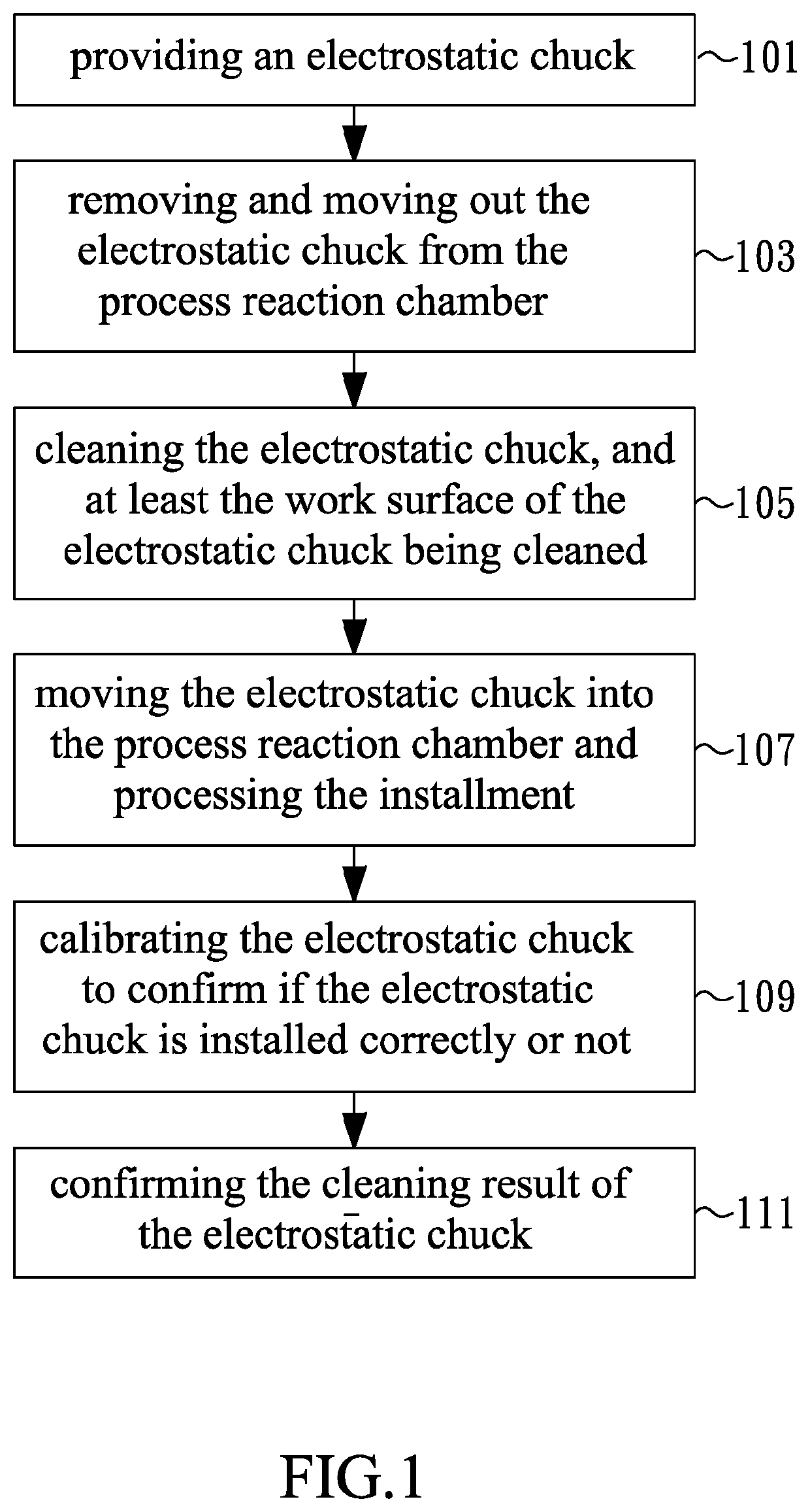
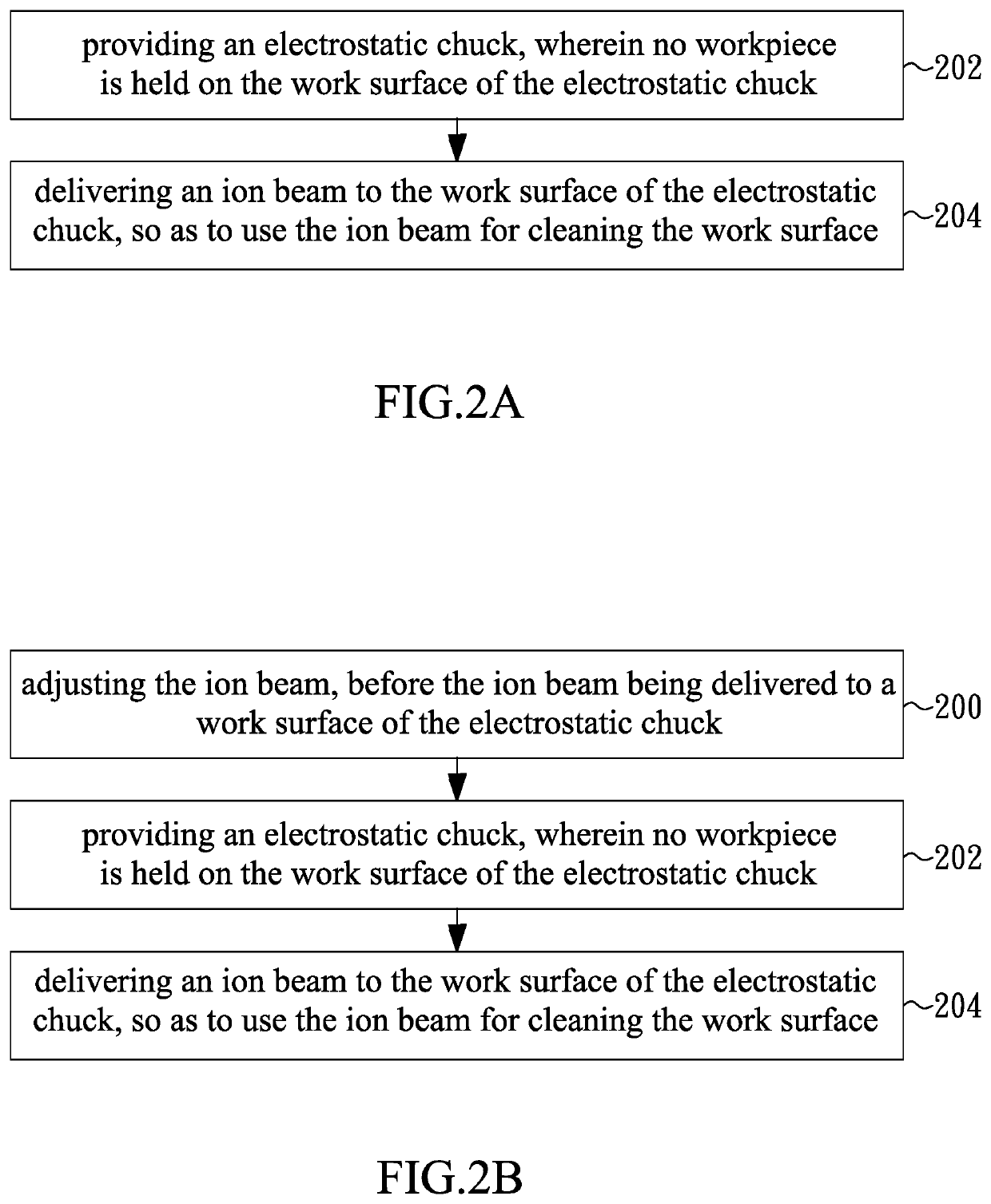
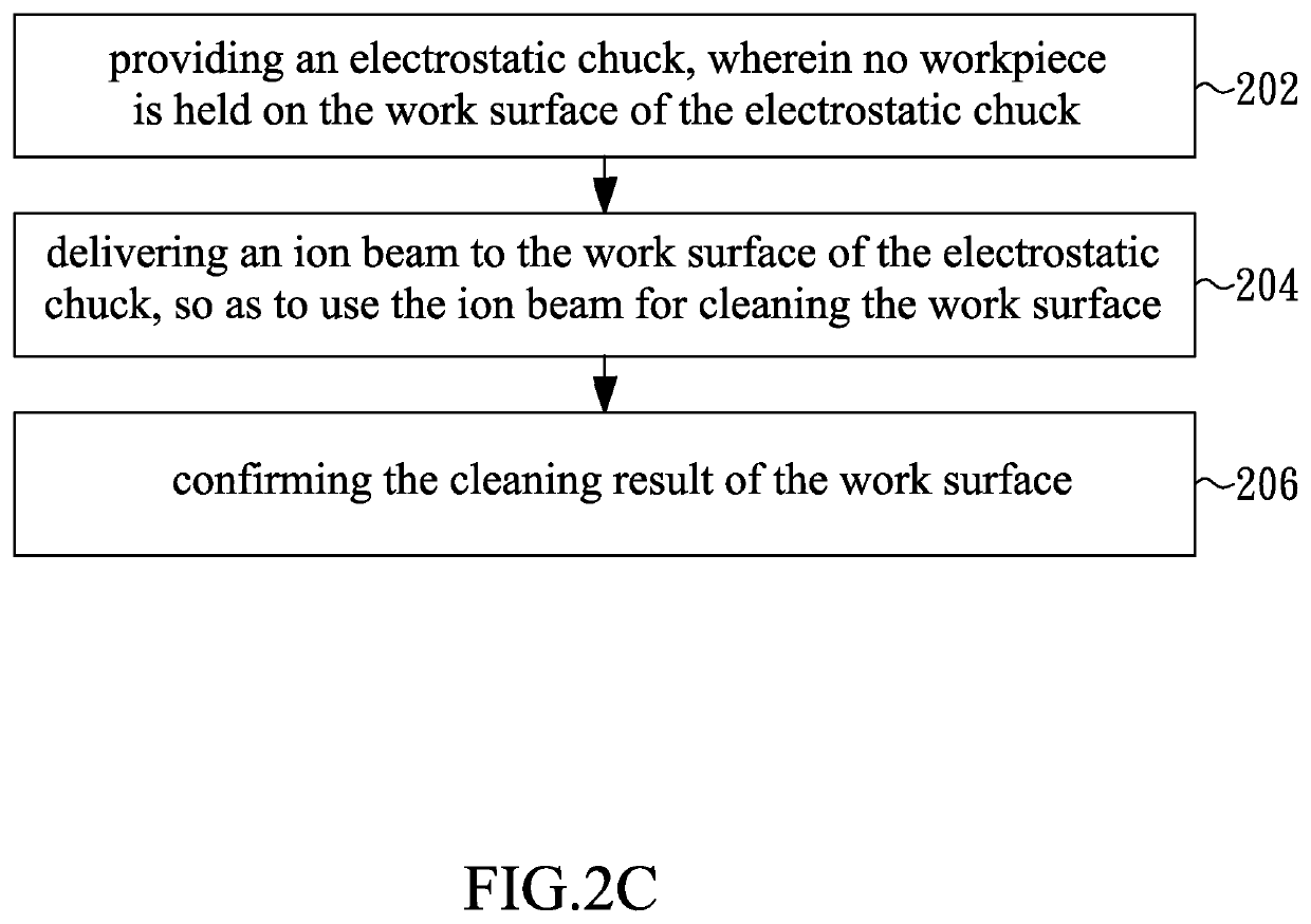
Method of cleaning electrostatic chuck
PatentActiveUS10699876B2
Innovation
- A method involving the use of an ion beam to clean the work surface of the electrostatic chuck within the reaction chamber, adjusting beam parameters based on deposition structure and material to remove contamination through physical or chemical means without moving the chuck, thus maintaining vacuum and avoiding unnecessary machine testing.

Electrostatic chuck to limit particle deposits thereon
PatentActiveUS20070268650A1
Innovation
- An electrostatic chuck with a dielectric layer and electrodes configured to accept a DC voltage signal, repelling charged particles from its surface when not supporting a workpiece to prevent deposits, using either a Coulombic or Johnsen-Rahbek type configuration depending on charge migration properties.


Cleanroom Standards and Regulations for ESC Operations
Cleanroom standards and regulations form the foundational framework for maintaining contamination-free environments essential for electrostatic chuck operations in semiconductor manufacturing. The International Organization for Standardization (ISO) 14644 series establishes the primary classification system for cleanrooms, defining particle concentration limits and monitoring requirements. For ESC operations, Class 1 to Class 100 cleanrooms are typically required, with particle counts not exceeding 10 particles per cubic foot for 0.5-micron particles in the most stringent environments.
Federal Standard 209E, though superseded by ISO standards, continues to influence cleanroom design principles and provides historical context for contamination control methodologies. The standard emphasizes the critical relationship between airflow patterns, filtration efficiency, and particle removal rates, which directly impact ion contamination levels around electrostatic chuck systems.
Semiconductor industry-specific regulations, including SEMI standards, provide detailed guidelines for cleanroom operations in wafer fabrication environments. SEMI F57 addresses contamination control requirements for process equipment, while SEMI F21 establishes protocols for particle monitoring and measurement. These standards mandate continuous monitoring of airborne molecular contamination, including ionic species that can compromise ESC performance.
Regulatory compliance extends beyond particle control to encompass personnel protocols, material handling procedures, and equipment qualification requirements. Cleanroom garment specifications, entry and exit procedures, and training requirements are strictly defined to minimize human-induced contamination sources. Material compatibility standards ensure that all components introduced into the cleanroom environment meet outgassing and particle generation criteria.
Environmental monitoring protocols require real-time tracking of temperature, humidity, and differential pressure alongside particle counts. These parameters directly influence electrostatic behavior and ion mobility within the cleanroom atmosphere. Validation procedures mandate periodic certification of filtration systems, airflow uniformity, and recovery performance following contamination events.
Documentation and traceability requirements ensure comprehensive record-keeping of all cleanroom activities, enabling rapid identification of contamination sources and implementation of corrective measures. Regular audits and compliance assessments verify adherence to established protocols and identify opportunities for continuous improvement in contamination control strategies.
ESC Material Compatibility and Contamination Prevention Strategies
Material compatibility represents a fundamental cornerstone in preventing ion contamination within electrostatic chuck systems. The selection of appropriate materials for ESC construction directly influences the generation and migration of ionic species during plasma processing operations. Silicon carbide and aluminum nitride have emerged as preferred substrate materials due to their superior chemical inertness and thermal stability under harsh plasma environments. These materials exhibit minimal outgassing characteristics and reduced susceptibility to chemical etching, thereby limiting the release of metallic ions that could compromise wafer processing integrity.
Surface treatment methodologies play a crucial role in establishing contamination-resistant ESC interfaces. Advanced coating technologies, including plasma-enhanced chemical vapor deposition of silicon dioxide and silicon nitride layers, create protective barriers that prevent direct exposure of base materials to reactive plasma species. These engineered surfaces demonstrate enhanced resistance to fluorine-based chemistries commonly employed in semiconductor etching processes, significantly reducing the formation of volatile metal fluorides that contribute to ion contamination.
Dielectric layer optimization constitutes another critical prevention strategy, focusing on material purity and structural uniformity. High-purity alumina and polyimide dielectrics, processed under controlled atmospheric conditions, minimize the incorporation of mobile ionic impurities during manufacturing. The implementation of multi-layer dielectric architectures with alternating high and low permittivity materials creates effective ion migration barriers while maintaining electrostatic clamping performance.
Contamination prevention extends beyond material selection to encompass comprehensive surface preparation protocols. Ultra-clean manufacturing environments, combined with precision cleaning procedures utilizing deionized water rinses and plasma conditioning treatments, establish contamination-free initial conditions. Regular maintenance schedules incorporating specialized cleaning chemistries designed for ESC applications help maintain surface integrity throughout operational lifecycles.
Environmental control strategies complement material-based approaches by minimizing external contamination sources. Implementation of particle filtration systems, humidity control mechanisms, and chemical vapor monitoring ensures that ESC systems operate within specified cleanliness parameters, preventing the accumulation of ionic contaminants that could migrate into critical processing zones during subsequent wafer handling operations.
Unlock deeper insights with PatSnap Eureka Quick Research — get a full tech report to explore trends and direct your research. Try now!
Generate Your Research Report Instantly with AI Agent
Supercharge your innovation with PatSnap Eureka AI Agent Platform!