How to Reduce Thermocompression Bonding Defects in PCBs
APR 23, 20269 MIN READ
Generate Your Research Report Instantly with AI Agent
PatSnap Eureka helps you evaluate technical feasibility & market potential.
Thermocompression Bonding Background and Objectives
Thermocompression bonding has emerged as a critical interconnection technology in the electronics manufacturing industry, particularly for printed circuit board (PCB) assembly processes. This technique involves the application of controlled heat and pressure to create reliable electrical and mechanical connections between components and substrates. The process has evolved significantly since its introduction in the 1960s, transitioning from simple wire bonding applications to sophisticated flip-chip and advanced packaging solutions.
The historical development of thermocompression bonding can be traced through several key phases. Initially developed for semiconductor packaging, the technology gained prominence in the 1970s and 1980s as electronic devices became more compact and performance requirements increased. The advent of surface mount technology (SMT) in the 1990s further accelerated the adoption of thermocompression bonding techniques, as manufacturers sought more reliable alternatives to traditional soldering methods for fine-pitch applications.
Contemporary PCB manufacturing faces unprecedented challenges in achieving defect-free thermocompression bonds. The miniaturization trend has led to increasingly smaller bond pads, tighter pitch requirements, and more complex multilayer structures. These developments have intensified the criticality of process control and quality assurance in bonding operations. Modern applications span from consumer electronics requiring cost-effective solutions to aerospace and medical devices demanding ultra-high reliability standards.
The primary technical objectives driving current research and development efforts focus on achieving consistent bond quality while minimizing defect rates. Key performance targets include maintaining bond strength specifications across varying environmental conditions, ensuring electrical continuity throughout product lifecycles, and achieving process yields exceeding 99.9% for high-volume manufacturing applications.
Process optimization objectives encompass reducing cycle times while maintaining quality standards, implementing real-time monitoring capabilities for defect prevention, and developing adaptive control systems that can compensate for material variations and environmental fluctuations. These goals align with industry demands for increased throughput and reduced manufacturing costs without compromising reliability.
The strategic importance of addressing thermocompression bonding defects extends beyond immediate quality concerns. As electronic systems become more integrated and failure-sensitive, the reliability of individual interconnections directly impacts overall system performance and customer satisfaction, making defect reduction a critical competitive advantage in the electronics manufacturing sector.
Market Demand for High-Quality PCB Assembly
The global electronics industry's relentless pursuit of miniaturization and enhanced performance has created unprecedented demand for high-quality PCB assembly solutions. Modern electronic devices, from smartphones to automotive control systems, require increasingly sophisticated circuit boards with higher component densities and more complex interconnection patterns. This evolution has made thermocompression bonding a critical process in PCB manufacturing, where even minor defects can compromise entire product functionality.
Consumer electronics manufacturers face mounting pressure to deliver products with zero-defect tolerance while maintaining competitive pricing. The proliferation of Internet of Things devices, 5G infrastructure, and electric vehicles has amplified the need for reliable PCB assemblies that can withstand harsh operating conditions. These applications demand superior electrical connectivity and mechanical stability, making defect-free thermocompression bonding essential for market success.
The automotive sector represents a particularly demanding market segment, where PCB assembly quality directly impacts safety-critical systems. Advanced driver assistance systems, engine control units, and battery management systems require PCBs with exceptional reliability standards. Defective thermocompression bonds in these applications can lead to catastrophic failures, driving automotive manufacturers to seek suppliers with proven defect reduction capabilities.
Medical device manufacturers constitute another high-value market segment with stringent quality requirements. Implantable devices, diagnostic equipment, and life-support systems demand PCB assemblies with extraordinary reliability and longevity. The regulatory environment in medical electronics creates substantial liability risks for defective products, making quality assurance paramount for market participation.
Aerospace and defense applications represent the premium tier of PCB assembly markets, where performance requirements often exceed commercial standards. These sectors demand PCBs capable of operating in extreme environments while maintaining perfect functionality. The high-value nature of aerospace and defense contracts makes investment in defect reduction technologies economically attractive for specialized manufacturers.
The emergence of artificial intelligence and machine learning applications has created new market opportunities for high-performance PCB assemblies. Data centers, edge computing devices, and AI accelerators require PCBs with exceptional thermal management and signal integrity characteristics. These applications often involve high-power components that stress thermocompression bonds, making defect prevention crucial for market competitiveness.
Current Bonding Defects and Technical Challenges
Thermocompression bonding in PCB manufacturing faces several critical defects that significantly impact product reliability and yield rates. The most prevalent defect is incomplete bonding, where insufficient heat or pressure results in weak interconnections between components and substrates. This manifests as poor electrical conductivity, intermittent connections, or complete circuit failures during operational stress testing.
Delamination represents another major challenge, occurring when thermal expansion mismatches between different materials cause separation at bonding interfaces. This defect is particularly problematic in multilayer PCBs where copper traces, dielectric materials, and solder masks exhibit different thermal coefficients. The resulting stress concentrations lead to progressive failure modes that compromise long-term reliability.
Void formation during the bonding process creates significant quality concerns. These voids, typically ranging from microscopic bubbles to larger cavities, form due to trapped gases, moisture, or contamination at bonding surfaces. Voids reduce effective bonding area, create stress concentration points, and can propagate under thermal cycling conditions, ultimately leading to catastrophic failures.
Overheating damage presents a complex technical challenge where excessive temperature or prolonged exposure causes material degradation. This includes copper oxidation, substrate charring, and polymer decomposition in flexible circuits. The narrow process window between insufficient bonding and thermal damage requires precise control systems that many manufacturing facilities struggle to maintain consistently.
Contamination-related defects stem from surface preparation inadequacies, including residual flux, oxidation layers, or particulate matter. These contaminants prevent proper metallurgical bonding and create weak interfaces susceptible to corrosion and mechanical failure. The challenge intensifies with miniaturization trends demanding higher precision in cleaning processes.
Pressure distribution non-uniformity across bonding surfaces creates localized defects where some areas experience insufficient compression while others suffer from excessive stress. This challenge is amplified in high-density interconnect designs where component height variations and substrate warpage complicate uniform pressure application.
Temperature gradient control remains a persistent technical hurdle, particularly in large format PCBs where maintaining uniform heating across the entire assembly proves difficult. Thermal imaging studies reveal significant temperature variations that correlate directly with bonding quality inconsistencies and defect distribution patterns.
Existing Defect Reduction Solutions
01 Detection and inspection methods for thermocompression bonding defects
Various detection and inspection techniques can be employed to identify defects in thermocompression bonding processes. These methods include optical inspection systems, X-ray imaging, ultrasonic testing, and automated vision systems that can detect voids, cracks, delamination, and misalignment issues. Advanced inspection technologies enable real-time monitoring and quality control during the bonding process, allowing for early detection of defects before they lead to product failure.- Detection and inspection methods for thermocompression bonding defects: Various detection and inspection techniques can be employed to identify defects in thermocompression bonding processes. These methods include optical inspection systems, X-ray imaging, ultrasonic testing, and automated vision systems that can detect voids, delamination, misalignment, and other bonding irregularities. Advanced inspection methods enable real-time monitoring and quality control during the bonding process to ensure proper bond formation and reliability.
- Process parameter optimization to prevent bonding defects: Controlling and optimizing key process parameters is critical for preventing thermocompression bonding defects. Important parameters include bonding temperature, pressure, dwell time, and heating rate. Proper calibration and control of these parameters help prevent common defects such as insufficient bonding, excessive deformation, cracking, and non-uniform bond formation. Process monitoring systems and feedback control mechanisms can be implemented to maintain optimal bonding conditions.
- Material selection and surface preparation techniques: The selection of appropriate bonding materials and proper surface preparation are essential for achieving defect-free thermocompression bonds. Surface cleaning, plasma treatment, and chemical modification can improve bonding interface quality by removing contaminants and enhancing surface energy. Material compatibility, thermal expansion matching, and surface roughness control help minimize stress-related defects and improve bond strength and reliability.
- Equipment design and tooling improvements: Advanced bonding equipment design and specialized tooling can significantly reduce thermocompression bonding defects. Features include precision temperature control systems, uniform pressure distribution mechanisms, alignment systems, and anti-contamination measures. Improved bonding head design, substrate holding fixtures, and thermal management systems help ensure consistent bonding quality and minimize defects caused by equipment limitations.
- Defect repair and rework methods: When thermocompression bonding defects occur, various repair and rework techniques can be applied to salvage defective assemblies. Methods include localized reheating and rebonding, underfill application to compensate for voids, and selective removal and replacement of defective bonds. Understanding the root causes of defects enables the development of effective repair strategies while maintaining the integrity of surrounding components and minimizing additional damage during rework operations.
02 Process parameter optimization to prevent bonding defects
Controlling and optimizing process parameters is critical for preventing thermocompression bonding defects. Key parameters include bonding temperature, pressure, time, and heating rate. Proper control of these variables ensures adequate material flow, prevents overheating or underheating, and achieves optimal bond strength. Process monitoring systems and feedback control mechanisms can be implemented to maintain consistent bonding conditions and minimize defect formation.Expand Specific Solutions03 Material selection and surface preparation techniques
The selection of appropriate bonding materials and proper surface preparation are essential for reducing thermocompression bonding defects. Surface cleaning, plasma treatment, and chemical modification can improve adhesion and eliminate contaminants that may cause voids or weak bonds. Material compatibility, thermal expansion coefficients, and surface roughness must be considered to ensure reliable bonding and prevent delamination or cracking.Expand Specific Solutions04 Equipment design and tooling improvements
Advanced equipment design and specialized tooling can significantly reduce thermocompression bonding defects. This includes precision alignment systems, uniform pressure distribution mechanisms, controlled heating elements, and anti-contamination features. Improved bonding head designs, substrate holders, and force control systems help maintain consistent bonding conditions across the entire bonding area, minimizing defects such as non-uniform bonds, tilting, or incomplete bonding.Expand Specific Solutions05 Defect repair and rework methods
When thermocompression bonding defects occur, various repair and rework techniques can be applied to salvage defective products. These methods include localized reheating and rebonding, removal and replacement of defective bonds, application of underfill materials, and post-bonding treatments. Specialized equipment and procedures have been developed to enable selective repair of bonding defects while minimizing damage to surrounding areas and maintaining product reliability.Expand Specific Solutions
Key Players in PCB Bonding Equipment Industry
The thermocompression bonding defect reduction market represents a mature yet evolving segment within the broader semiconductor packaging and PCB manufacturing industry. The market is currently in a consolidation phase, driven by increasing demand for miniaturization and higher reliability in electronic devices. Major players like Intel Corp., Taiwan Semiconductor Manufacturing Co., Samsung Electronics, and Texas Instruments dominate through advanced process technologies and substantial R&D investments. Specialized materials companies including Dexerials Corp., Indium Corporation, and Namics Corp. provide critical bonding materials and adhesives. The technology maturity varies significantly across applications, with established players like Panasonic Holdings and Sharp Corp. offering proven solutions, while emerging companies focus on next-generation materials and processes. The competitive landscape is characterized by vertical integration among semiconductor giants and strategic partnerships with specialized material suppliers to address evolving thermal management and reliability challenges.
Intel Corp.
Technical Solution: Intel employs advanced process control and real-time monitoring systems to minimize thermocompression bonding defects in their semiconductor packaging operations. Their approach includes precise temperature and pressure control algorithms, optimized bonding force profiles, and automated defect detection systems using machine vision technology. The company utilizes specialized bonding equipment with closed-loop feedback control to maintain consistent bonding parameters throughout the process. Intel also implements statistical process control methods to identify and correct process variations before they lead to defects, ensuring high yield rates in their advanced packaging technologies.
Strengths: Industry-leading process control technology and extensive R&D resources. Weaknesses: Solutions may be cost-prohibitive for smaller manufacturers and require significant infrastructure investment.
Taiwan Semiconductor Manufacturing Co., Ltd.
Technical Solution: TSMC has developed comprehensive defect reduction strategies for thermocompression bonding in advanced packaging applications, particularly for their CoWoS (Chip-on-Wafer-on-Substrate) technology. Their methodology includes optimized bonding temperature profiles, precise alignment systems, and advanced surface preparation techniques to ensure clean bonding interfaces. TSMC employs multi-stage quality control processes with in-line inspection systems that can detect micro-voids and bonding irregularities in real-time. The company also utilizes predictive maintenance algorithms to prevent equipment-related defects and maintains strict environmental controls to minimize contamination during the bonding process.
Strengths: World-class manufacturing expertise and cutting-edge advanced packaging capabilities. Weaknesses: Highly specialized solutions that may not be easily transferable to different manufacturing environments.
Core Patents in Bonding Process Optimization
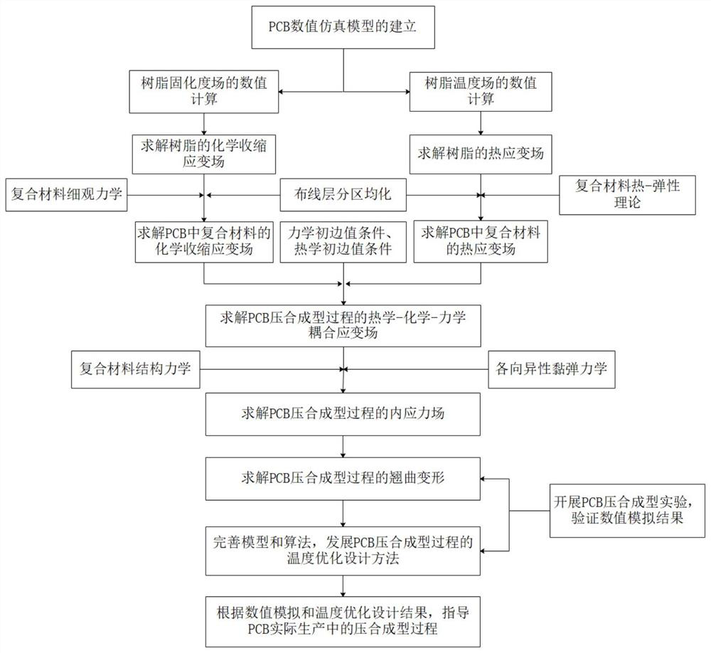
Temperature optimization design method and system for reducing buckling deformation of PCB after lamination
PatentActiveCN114189999A
Innovation
- Using numerical simulation technology, through layered modeling and thermal-chemical-mechanical coupling methods, the temperature field and curing degree field during the PCB lamination process are calculated, and the maximum curing temperature in the lamination process is optimized to reduce warpage deformation.


Contaminant control in thermocompression bonding of semiconductors and associated systems and methods
PatentActiveUS11908828B2
Innovation
- A supplemental vacuum source is applied around the bondhead to draw in and retain offgassing vapors, reducing contamination and improving die placement accuracy and interconnect reliability by creating a path for vaporized bonding material to be withdrawn before it reaches the bondhead, thereby extending equipment life and reducing manufacturing costs.


Quality Standards and Certification Requirements
The quality standards and certification requirements for thermocompression bonding in PCB manufacturing are governed by multiple international and industry-specific frameworks that establish critical parameters for defect prevention and process validation. These standards provide comprehensive guidelines for material specifications, process controls, and acceptance criteria that directly impact bonding quality and reliability.
IPC standards serve as the primary foundation for PCB thermocompression bonding requirements, with IPC-A-610 defining acceptability criteria for electronic assemblies and IPC-6012 establishing performance specifications for rigid printed boards. These standards specify critical parameters including bond strength requirements, void percentage limitations, and visual inspection criteria for identifying potential defects such as delamination, insufficient bonding, and material degradation.
ISO 9001 quality management system requirements mandate documented procedures for process control, traceability, and continuous improvement in thermocompression bonding operations. The standard emphasizes statistical process control implementation, requiring manufacturers to establish control limits for critical parameters such as temperature uniformity, pressure distribution, and cycle time consistency to minimize defect occurrence.
Military and aerospace applications demand compliance with MIL-PRF-31032 and IPC-6013 Class 3 requirements, which impose stringent controls on material purity, process validation, and reliability testing. These specifications require extensive qualification testing including thermal cycling, vibration resistance, and long-term reliability assessments to ensure bonding integrity under extreme operating conditions.
Automotive industry standards, particularly IATF 16949 and AEC-Q100, establish additional requirements for process capability studies and failure mode analysis specific to thermocompression bonding applications. These standards mandate advanced process control techniques including real-time monitoring systems and predictive maintenance protocols to prevent defect formation.
Medical device applications must comply with ISO 13485 requirements, which emphasize risk management and validation protocols for critical bonding processes. The standard requires comprehensive documentation of process parameters, material traceability, and statistical validation of defect reduction measures to ensure patient safety and device reliability throughout the product lifecycle.
Environmental Impact of Bonding Process Improvements
The implementation of advanced thermocompression bonding process improvements in PCB manufacturing presents significant environmental benefits that extend beyond traditional quality metrics. Modern bonding technologies demonstrate substantial reductions in energy consumption through optimized temperature profiles and shorter processing cycles, directly contributing to decreased carbon footprint in electronics manufacturing facilities.
Enhanced process control systems enable precise temperature and pressure management, eliminating the need for excessive heating cycles that traditionally compensated for process variability. This optimization reduces overall energy consumption by approximately 15-25% compared to conventional bonding approaches, while simultaneously improving yield rates and reducing material waste.
The reduction of bonding defects through improved process parameters directly correlates with decreased electronic waste generation. Higher first-pass yield rates mean fewer rejected PCBs requiring disposal or energy-intensive rework processes. This improvement is particularly significant given the complex material composition of modern PCBs, which contain various metals and substrates that pose environmental challenges when improperly disposed.
Advanced flux formulations and cleaning processes associated with improved bonding techniques utilize more environmentally friendly chemical compositions. These newer formulations reduce volatile organic compound emissions and minimize the use of hazardous substances, aligning with global environmental regulations such as RoHS and REACH directives.
Temperature profiling optimization and real-time monitoring systems contribute to reduced thermal stress on components, extending product lifespan and reducing the frequency of premature failures. This longevity improvement directly impacts the electronics industry's environmental footprint by decreasing replacement cycles and associated manufacturing demands.
The integration of predictive maintenance capabilities in modern bonding equipment reduces unexpected failures and associated waste streams. Preventive approaches minimize emergency repairs that often require expedited material sourcing and disposal of damaged components, further supporting sustainable manufacturing practices in the electronics industry.
Unlock deeper insights with PatSnap Eureka Quick Research — get a full tech report to explore trends and direct your research. Try now!
Generate Your Research Report Instantly with AI Agent
Supercharge your innovation with PatSnap Eureka AI Agent Platform!