

Implementing Control Measures For Photolithography Process Uniformity
FEB 10, 20268 MIN READ
Generate Your Research Report Instantly with AI Agent
PatSnap Eureka helps you evaluate technical feasibility & market potential.
Photolithography Uniformity Control Background and Objectives
Photolithography stands as the cornerstone technology in semiconductor manufacturing, enabling the transfer of intricate circuit patterns onto silicon wafers through precise light exposure and chemical processing. Since its inception in the 1960s, this technology has evolved from simple contact printing to advanced extreme ultraviolet lithography, consistently pushing the boundaries of feature size reduction. The continuous scaling down of semiconductor devices, following Moore's Law, has placed unprecedented demands on photolithography process control, where even nanometer-scale variations can significantly impact device performance and manufacturing yield.
Process uniformity in photolithography refers to the consistency of pattern dimensions, critical dimensions, and overlay accuracy across the entire wafer surface and between different wafers in production batches. As semiconductor nodes advance toward 3nm and beyond, the tolerance for process variation has shrunk dramatically, with critical dimension uniformity requirements now measured in fractions of a nanometer. Non-uniformities can arise from multiple sources including optical aberrations, resist coating thickness variations, thermal gradients during exposure and post-exposure bake, and chemical concentration differences during development.
The primary objective of implementing control measures for photolithography process uniformity is to achieve consistent pattern fidelity across all exposure fields and wafers, thereby maximizing device yield and performance predictability. This encompasses maintaining tight control over critical dimensions, ensuring precise overlay alignment between successive lithography layers, and minimizing defect density. Advanced control strategies aim to compensate for systematic variations through predictive modeling and real-time adjustments, while simultaneously reducing random variations through enhanced process stability.
Furthermore, these control measures must address the increasing complexity of multi-patterning techniques required at advanced nodes, where a single device layer may require multiple lithography and etching steps. The integration of computational lithography, advanced metrology systems, and machine learning algorithms represents the modern approach to achieving the stringent uniformity specifications demanded by current and future semiconductor manufacturing processes.
Market Demand for Advanced Lithography Process Control
The semiconductor industry's relentless pursuit of smaller feature sizes and higher device densities has created unprecedented demand for advanced lithography process control solutions. As manufacturers transition to extreme ultraviolet lithography and push the boundaries of deep ultraviolet technology, maintaining process uniformity across wafers has become a critical bottleneck affecting yield rates and production economics. The market for sophisticated control measures addressing photolithography uniformity challenges is experiencing robust growth driven by the proliferation of advanced nodes below seven nanometers and the expanding adoption of three-dimensional integrated circuit architectures.
Major semiconductor fabrication facilities are investing heavily in process control infrastructure to meet stringent uniformity specifications required by leading-edge applications. The automotive electronics sector, particularly electric vehicles and autonomous driving systems, demands exceptionally high reliability standards that necessitate superior lithography uniformity. Similarly, the artificial intelligence and high-performance computing markets require chips with billions of transistors manufactured with minimal variation, directly translating into increased demand for advanced control methodologies.
The economic implications of lithography non-uniformity are substantial, as even minor deviations can result in significant yield losses and increased manufacturing costs. Foundries and integrated device manufacturers recognize that implementing comprehensive control measures represents a strategic investment rather than an operational expense. This perspective shift has accelerated market adoption of real-time monitoring systems, advanced metrology tools, and predictive analytics platforms specifically designed for photolithography process optimization.
Emerging applications in photonics, quantum computing, and advanced packaging technologies are creating new market segments with unique uniformity requirements. These specialized applications often demand customized control solutions that extend beyond traditional semiconductor manufacturing parameters. The convergence of artificial intelligence with process control systems is opening additional market opportunities, as machine learning algorithms enable more sophisticated pattern recognition and predictive maintenance capabilities that enhance overall process uniformity and equipment utilization rates.
Current Uniformity Challenges in Photolithography Systems
Photolithography systems face multiple uniformity challenges that directly impact semiconductor manufacturing yield and device performance. Critical dimension uniformity across the wafer surface remains a primary concern, as variations in feature dimensions can lead to inconsistent electrical characteristics and reduced chip functionality. These variations stem from complex interactions between optical systems, resist chemistry, and substrate properties, making them difficult to predict and control systematically.
Exposure dose uniformity presents another significant challenge, particularly as wafer sizes increase and feature dimensions shrink. Non-uniform light intensity distribution across the exposure field creates localized variations in pattern transfer fidelity. This issue becomes more pronounced at advanced technology nodes where the process window narrows considerably. Scanner illumination systems must maintain precise intensity control while compensating for lens aberrations and field curvature effects that naturally occur in high numerical aperture optical systems.
Focus uniformity across the wafer topography introduces additional complexity, especially for devices with multiple patterning layers and varying substrate heights. Wafer flatness deviations, chuck-induced distortions, and thermal expansion during processing contribute to focus errors that compromise pattern resolution. Advanced lithography systems operating at extreme ultraviolet wavelengths face heightened sensitivity to these focus variations due to their extremely shallow depth of focus requirements.
Overlay accuracy between successive lithography layers represents a critical uniformity challenge that directly affects device yield. Systematic and random overlay errors arise from wafer stage positioning inaccuracies, lens distortions, thermal processing effects, and wafer deformation. As design rules tighten below ten nanometers, overlay budgets shrink proportionally, demanding sub-nanometer control across the entire wafer surface.
Resist coating uniformity and post-exposure bake temperature distribution further complicate the uniformity equation. Edge bead effects, spin coating dynamics, and hotplate temperature gradients create systematic patterns of process variation. These factors interact with exposure and focus non-uniformities, amplifying their impact on final pattern quality and making root cause analysis particularly challenging for process engineers.
Existing Process Uniformity Control Methodologies
01 Exposure dose control and optimization
Controlling and optimizing the exposure dose in photolithography processes is critical for achieving uniform pattern transfer across the wafer. This involves precise calibration of light sources, adjustment of exposure parameters, and implementation of dose correction algorithms to compensate for variations in resist sensitivity and substrate reflectivity. Advanced monitoring systems can measure and adjust exposure doses in real-time to maintain consistency across different regions of the wafer.- Exposure dose control and optimization: Controlling and optimizing the exposure dose during photolithography is critical for achieving uniform pattern transfer across the wafer. This involves precise calibration of light sources, adjustment of exposure parameters, and implementation of dose correction algorithms to compensate for variations in resist sensitivity and substrate reflectivity. Advanced monitoring systems can measure and adjust exposure doses in real-time to maintain consistency across different regions of the wafer.
- Focus control and leveling techniques: Maintaining optimal focus across the entire wafer surface is essential for photolithography uniformity. This includes wafer leveling systems, auto-focus mechanisms, and topography compensation methods. Advanced systems employ multiple measurement points to create a focus map and adjust the focal plane dynamically during exposure to account for wafer warpage, thickness variations, and chuck flatness issues.
- Illumination uniformity optimization: Achieving uniform illumination across the exposure field is fundamental to photolithography process uniformity. This involves optical system design improvements, illumination source optimization, and the use of correction elements to eliminate intensity variations. Techniques include pupil shaping, aperture optimization, and the implementation of uniformity correction filters to ensure consistent light distribution across the entire exposure area.
- Reticle and mask optimization: The quality and characteristics of photomasks directly impact pattern uniformity. This includes mask error correction, optical proximity correction, and compensation for mask-induced variations. Advanced techniques involve mask bias optimization, phase-shifting mask technology, and the use of computational lithography methods to pre-compensate for known systematic variations in the lithography process.
- Process monitoring and feedback control: Real-time monitoring and closed-loop feedback control systems are essential for maintaining photolithography uniformity. This includes in-situ metrology, overlay measurement systems, and critical dimension monitoring across the wafer. Advanced process control utilizes statistical analysis, machine learning algorithms, and predictive modeling to identify and correct process variations before they impact product yield.
02 Focus control and leveling techniques
Maintaining optimal focus across the entire wafer surface is essential for photolithography uniformity. This includes wafer leveling systems, auto-focus mechanisms, and topography compensation methods. Advanced systems employ multiple measurement points to create focus maps and dynamically adjust the focal plane during exposure to account for wafer warpage, thickness variations, and chuck flatness issues.Expand Specific Solutions03 Illumination uniformity optimization
Achieving uniform illumination across the exposure field is fundamental to photolithography process uniformity. This involves optical system design improvements, pupil shaping techniques, and illumination source optimization. Methods include using diffusers, integrators, and compensation filters to eliminate intensity variations and hotspots in the illumination pattern, ensuring consistent energy delivery across the entire exposure area.Expand Specific Solutions04 Resist coating and development uniformity
Uniform application and processing of photoresist materials directly impacts pattern uniformity. This encompasses spin coating optimization, edge bead removal techniques, post-apply bake uniformity, and development process control. Advanced methods include dynamic dispense control, multi-zone temperature management during baking, and optimized development time and agitation to ensure consistent resist thickness and processing across the wafer.Expand Specific Solutions05 Overlay and alignment accuracy improvement
Precise overlay control and alignment between successive lithography layers is crucial for overall process uniformity. This includes advanced metrology systems, alignment mark optimization, and correction algorithms for distortion and magnification errors. Techniques involve high-precision stage control, interferometric positioning systems, and computational methods to compensate for wafer expansion, process-induced shifts, and tool-to-tool variations.Expand Specific Solutions
Major Players in Photolithography Equipment and Solutions
The photolithography process uniformity control market represents a mature yet rapidly evolving sector within semiconductor manufacturing, driven by escalating demands for advanced node production and extreme ultraviolet (EUV) technology adoption. The industry demonstrates a consolidated competitive landscape dominated by established equipment manufacturers like ASML Holding NV and ASML Netherlands BV, who lead in cutting-edge lithography systems, alongside Tokyo Electron Ltd. and Lam Research Corp. providing complementary process equipment. Major foundries including Taiwan Semiconductor Manufacturing Co., Samsung Electronics, and GLOBALFOUNDRIES drive technological requirements, while Chinese players like SMIC and ChangXin Memory Technologies represent emerging regional competition. Technology maturity varies significantly across segments, with companies like Synopsys providing advanced computational lithography solutions and Nova Ltd. offering sophisticated metrology capabilities, while Shanghai Microelectronics Equipment pursues domestic alternatives. The market exhibits strong growth potential, particularly in advanced packaging and sub-3nm processes, though geopolitical factors increasingly influence competitive dynamics and supply chain strategies.
ASML Holding NV
Technical Solution: ASML implements advanced control measures for photolithography process uniformity through their integrated metrology and computational lithography solutions. Their approach combines real-time overlay control systems with dose correction algorithms to maintain critical dimension uniformity across wafers. The company utilizes advanced sensors embedded in their EUV and DUV lithography systems to monitor process parameters continuously, enabling dynamic adjustments during exposure. Their Holistic Lithography platform integrates machine learning algorithms to predict and compensate for process variations, achieving overlay accuracy below 1.5nm and CD uniformity within 2nm across 300mm wafers. The system employs wafer-level and field-level corrections using feedback from previous exposures, combined with predictive modeling based on thermal effects, lens aberrations, and reticle heating patterns.
Strengths: Industry-leading overlay accuracy and CD uniformity control; comprehensive integration of metrology and correction systems; advanced EUV process control capabilities. Weaknesses: High system complexity requiring specialized expertise; significant capital investment; dependency on proprietary algorithms and hardware integration.
Taiwan Semiconductor Manufacturing Co., Ltd.
Technical Solution: TSMC implements comprehensive process uniformity control through their Advanced Process Control (APC) framework, which integrates statistical process control with run-to-run feedback mechanisms. Their approach utilizes extensive in-line metrology stations measuring critical dimensions, overlay, and film thickness at multiple process stages. TSMC employs sophisticated dose and focus control strategies, including scanner matching programs that ensure consistent performance across multiple lithography tools. Their uniformity control system incorporates machine learning models trained on historical process data to predict and prevent excursions before they occur. The company implements advanced reticle heating compensation algorithms and uses computational lithography techniques including optical proximity correction (OPC) and source-mask optimization (SMO) to enhance pattern fidelity. Their process control achieves CD uniformity better than 1.8nm (3-sigma) for advanced nodes, with overlay control below 2nm for critical layers in their 3nm and 5nm processes.
Strengths: Extensive manufacturing experience with proven high-volume production control; comprehensive data analytics infrastructure; excellent cross-tool matching capabilities. Weaknesses: Solutions are primarily internally developed and not commercially available; significant infrastructure investment required; complexity increases with advanced node requirements.
Core Technologies in Lithography Uniformity Enhancement
Method and apparatus for controlling light intensity and for exposing a semiconductor substrate
PatentInactiveUS20070190438A1
Innovation
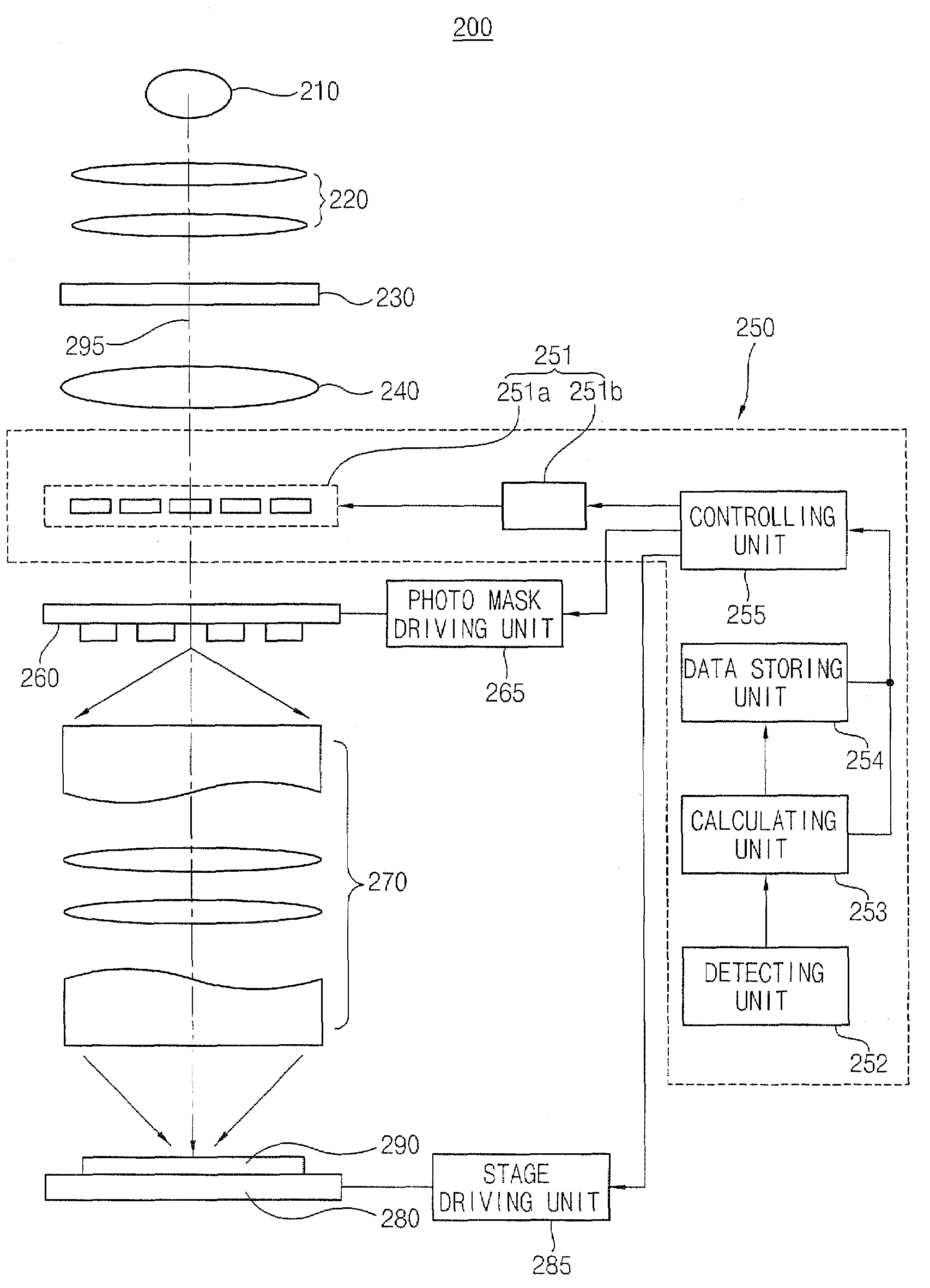
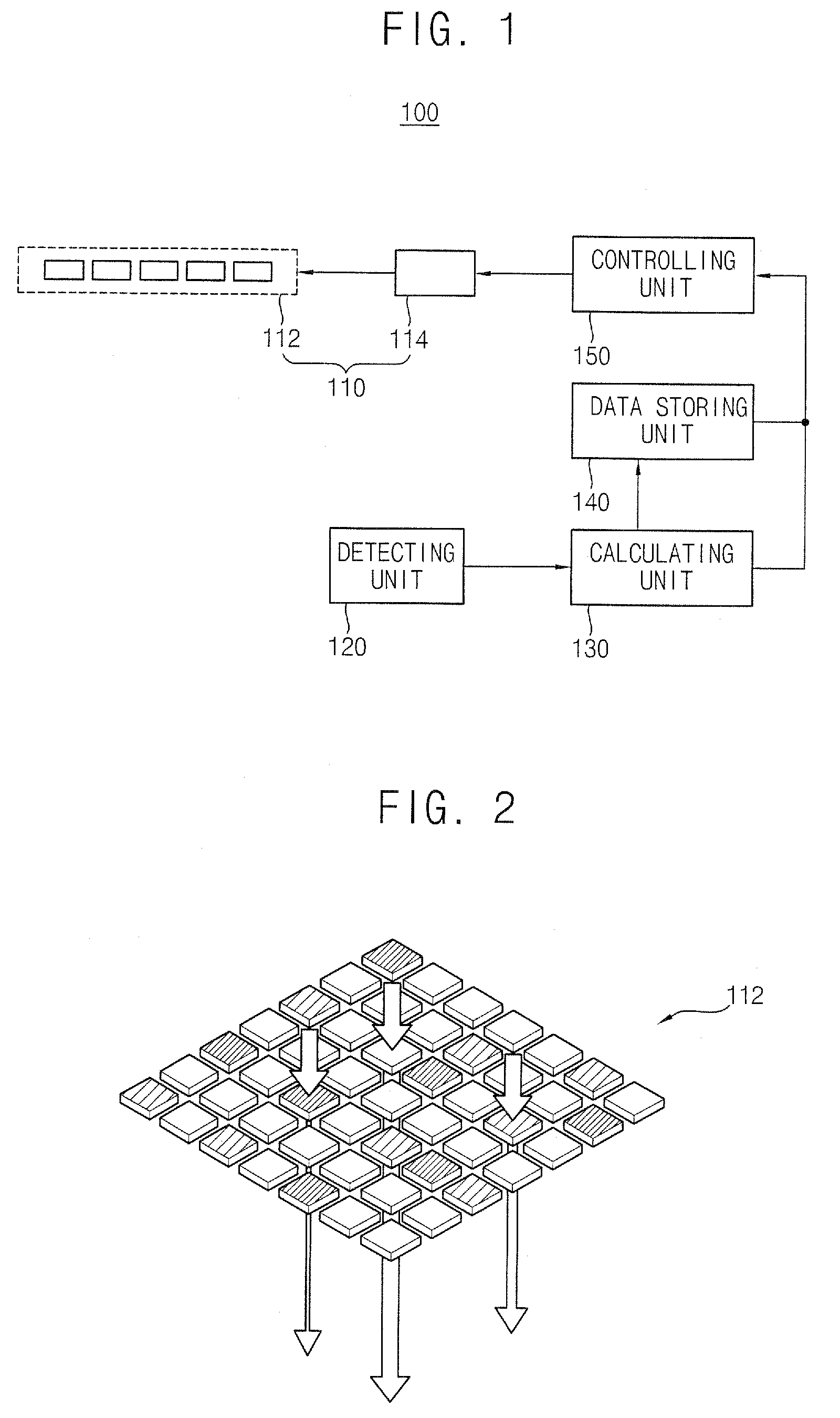
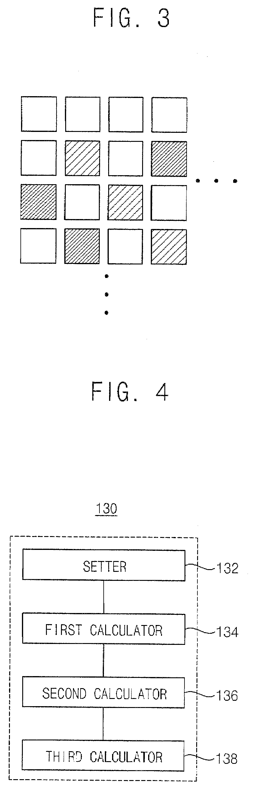
- A method and apparatus that control light intensity by detecting critical dimension distributions on semiconductor substrates, calculating and adjusting the intensity distribution of illumination based on the photo mask regions, using a light transmission element array with variable transmissivity to convert the first illumination into a second illumination with uniform critical dimensions, thereby forming patterns with consistent dimensions.

Method and apparatus for controlling photolithography overlay registration incorporating feedforward overlay information
PatentInactiveUS6897075B2
Innovation
- A method and apparatus for controlling photolithography overlay registration using feedforward overlay information, where a controller adjusts the operating recipe for a photolithography stepper based on measurements from an overlay metrology tool, incorporating both feedback and feedforward data to account for wafer-to-wafer and lot-to-lot variations, thereby reducing overlay errors.


Metrology and Monitoring Systems for Uniformity Assessment
Effective metrology and monitoring systems form the cornerstone of achieving and maintaining photolithography process uniformity across semiconductor manufacturing operations. These systems provide real-time and post-process measurements that enable precise characterization of critical parameters including critical dimension uniformity, overlay accuracy, and film thickness variations across wafer surfaces. Advanced optical metrology tools such as scatterometry and spectroscopic ellipsometry have become indispensable for non-destructive, high-throughput measurements that capture spatial variations with nanometer-level precision. These instruments generate comprehensive uniformity maps that reveal systematic patterns and localized defects, enabling rapid identification of process deviations.
Modern monitoring architectures integrate multiple measurement modalities to provide comprehensive uniformity assessment. In-line metrology stations positioned at strategic process steps capture data from representative wafer sites, while advanced sampling strategies balance measurement density with throughput requirements. Emerging technologies such as on-product overlay metrology and high-resolution imaging systems enable direct assessment of pattern fidelity and placement accuracy, providing immediate feedback on lithography performance.
The integration of sensor networks within lithography equipment itself represents a significant advancement in real-time process monitoring. Environmental sensors tracking temperature, humidity, and vibration levels, combined with equipment-state monitors measuring lens aberrations, stage positioning accuracy, and illumination uniformity, create a multidimensional data stream that correlates equipment conditions with process outcomes. This sensor fusion approach enables predictive maintenance and proactive process adjustments before uniformity degradation occurs.
Data analytics platforms have evolved to handle the massive volumes of metrology data generated across production lines. Statistical process control algorithms automatically detect uniformity trends and trigger alerts when parameters drift beyond specification limits. Machine learning models trained on historical metrology data can predict uniformity outcomes based on equipment settings and environmental conditions, enabling feed-forward control strategies that preemptively adjust process parameters to maintain optimal uniformity across varying operational conditions.
Cost-Benefit Analysis of Uniformity Control Implementation
The implementation of control measures for photolithography process uniformity requires careful economic evaluation to justify capital investment and operational expenditures. Initial capital costs typically encompass advanced metrology equipment, real-time monitoring systems, and process control software, with investments ranging from several hundred thousand to millions of dollars depending on facility scale. These upfront expenses must be weighed against the substantial benefits derived from improved yield rates and reduced defect densities across wafer surfaces.
Operational cost considerations include increased maintenance requirements for precision equipment, additional personnel training programs, and ongoing calibration procedures. However, these recurring expenses are generally offset by significant reductions in material waste and rework costs. Enhanced uniformity control directly translates to higher first-pass yields, potentially improving production efficiency by 5-15% in mature manufacturing environments. This yield improvement alone can generate annual savings exceeding initial investment costs within 18-24 months for high-volume production facilities.
The financial benefits extend beyond direct cost savings to include enhanced product quality and reliability. Improved critical dimension uniformity enables tighter specification compliance, reducing customer returns and warranty claims. Additionally, superior process control capabilities provide competitive advantages in securing contracts for advanced node production, where uniformity requirements become increasingly stringent. Market positioning benefits can generate premium pricing opportunities and expanded customer base.
Risk mitigation represents another crucial benefit dimension. Robust uniformity control systems reduce exposure to costly production disruptions and yield excursions that can result in multi-million dollar losses during single incidents. The implementation of preventive control measures provides insurance against such catastrophic events while enabling faster root cause analysis and corrective action deployment.
Return on investment calculations must also account for scalability factors and technology lifecycle considerations. Modern control systems offer modular expansion capabilities, allowing incremental investment aligned with production volume growth. Furthermore, data analytics capabilities embedded in advanced control platforms generate valuable process insights that drive continuous improvement initiatives, creating compounding value over extended operational periods.
Unlock deeper insights with PatSnap Eureka Quick Research — get a full tech report to explore trends and direct your research. Try now!
Generate Your Research Report Instantly with AI Agent
Supercharge your innovation with PatSnap Eureka AI Agent Platform!