

Improve Photonic Tensor Core Yield Through Process Refinement Techniques
MAY 11, 20269 MIN READ
Generate Your Research Report Instantly with AI Agent
PatSnap Eureka helps you evaluate technical feasibility & market potential.
Photonic Tensor Core Development Background and Yield Targets
Photonic tensor cores represent a revolutionary convergence of optical computing and artificial intelligence acceleration technologies, emerging from decades of research in both photonics and neural network processing. The development trajectory began with early optical computing concepts in the 1980s, evolved through silicon photonics breakthroughs in the 2000s, and has recently accelerated with the explosive growth of AI workloads requiring massive parallel processing capabilities.
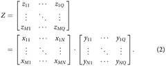
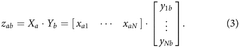
The fundamental principle underlying photonic tensor cores leverages the inherent parallelism of light to perform matrix multiplication operations at unprecedented speeds while consuming significantly less power than traditional electronic processors. These devices utilize wavelength division multiplexing, optical interference, and photodetection to execute tensor operations that form the backbone of modern deep learning algorithms.
Current photonic tensor core architectures face substantial yield challenges that significantly impact commercial viability. Manufacturing defects in silicon photonic waveguides, coupling losses between optical and electronic components, and thermal sensitivity variations contribute to yield rates typically ranging from 15% to 35% in early-stage production environments. These yield limitations stem from the precision requirements inherent in photonic device fabrication, where nanometer-scale variations can dramatically affect optical performance.
The strategic importance of improving photonic tensor core yield extends beyond immediate cost considerations. As AI workloads continue expanding exponentially, the energy efficiency advantages of photonic processing become increasingly critical for sustainable computing infrastructure. Traditional electronic AI accelerators face fundamental physical limitations in power consumption and heat dissipation that photonic solutions can potentially overcome.
Industry consensus establishes target yield improvements to achieve 70-85% production yields within the next three to five years. These targets align with commercial viability thresholds necessary for widespread adoption in data centers and edge computing applications. Achieving these yield targets requires systematic refinement of fabrication processes, enhanced quality control methodologies, and innovative design approaches that increase tolerance to manufacturing variations.
The economic implications of successful yield improvement are substantial, with potential cost reductions of 60-80% per functional device, making photonic tensor cores competitive with established electronic alternatives while delivering superior performance characteristics for specific AI workloads.
The fundamental principle underlying photonic tensor cores leverages the inherent parallelism of light to perform matrix multiplication operations at unprecedented speeds while consuming significantly less power than traditional electronic processors. These devices utilize wavelength division multiplexing, optical interference, and photodetection to execute tensor operations that form the backbone of modern deep learning algorithms.
Current photonic tensor core architectures face substantial yield challenges that significantly impact commercial viability. Manufacturing defects in silicon photonic waveguides, coupling losses between optical and electronic components, and thermal sensitivity variations contribute to yield rates typically ranging from 15% to 35% in early-stage production environments. These yield limitations stem from the precision requirements inherent in photonic device fabrication, where nanometer-scale variations can dramatically affect optical performance.
The strategic importance of improving photonic tensor core yield extends beyond immediate cost considerations. As AI workloads continue expanding exponentially, the energy efficiency advantages of photonic processing become increasingly critical for sustainable computing infrastructure. Traditional electronic AI accelerators face fundamental physical limitations in power consumption and heat dissipation that photonic solutions can potentially overcome.
Industry consensus establishes target yield improvements to achieve 70-85% production yields within the next three to five years. These targets align with commercial viability thresholds necessary for widespread adoption in data centers and edge computing applications. Achieving these yield targets requires systematic refinement of fabrication processes, enhanced quality control methodologies, and innovative design approaches that increase tolerance to manufacturing variations.
The economic implications of successful yield improvement are substantial, with potential cost reductions of 60-80% per functional device, making photonic tensor cores competitive with established electronic alternatives while delivering superior performance characteristics for specific AI workloads.
Market Demand for High-Performance Photonic AI Accelerators
The global artificial intelligence accelerator market is experiencing unprecedented growth, driven by the exponential increase in computational demands for machine learning workloads across diverse industries. Traditional electronic processors face fundamental limitations in power efficiency and processing speed when handling massive parallel computations required for neural network training and inference. This has created a substantial market opportunity for photonic AI accelerators, which leverage light-based computing to overcome the bandwidth and energy constraints of electronic systems.
Enterprise data centers represent the largest segment of demand for high-performance photonic AI accelerators. Cloud service providers are actively seeking solutions to reduce power consumption while maintaining computational throughput for AI workloads. The energy efficiency advantages of photonic tensor cores, which can perform matrix multiplications using optical interference patterns, align directly with sustainability goals and operational cost reduction objectives in large-scale computing facilities.
The autonomous vehicle industry presents another significant market driver for photonic AI acceleration technology. Real-time processing requirements for sensor fusion, object detection, and decision-making algorithms demand ultra-low latency computation that photonic systems can potentially deliver. The ability to process multiple data streams simultaneously through wavelength division multiplexing makes photonic tensor cores particularly attractive for automotive AI applications.
Telecommunications infrastructure modernization is creating additional demand for photonic AI accelerators. The deployment of intelligent network management systems, predictive maintenance algorithms, and dynamic resource allocation requires high-performance computing capabilities at edge locations. Photonic processors offer the potential for seamless integration with existing fiber optic networks while providing the computational power needed for distributed AI applications.
Financial services and high-frequency trading represent specialized but lucrative market segments for photonic AI technology. The speed-of-light processing capabilities inherent in photonic systems could provide competitive advantages in algorithmic trading and risk analysis applications where microsecond improvements translate to significant financial gains.
Manufacturing and industrial automation sectors are increasingly adopting AI-driven quality control and predictive maintenance systems. The harsh electromagnetic environments common in industrial settings make photonic processors attractive due to their inherent immunity to electromagnetic interference, creating demand for ruggedized photonic AI accelerator solutions.
However, market adoption faces challenges related to manufacturing yield and cost competitiveness. Current photonic tensor core production suffers from yield issues that impact commercial viability. Process refinement techniques that improve manufacturing consistency and reduce defect rates are essential for meeting market price expectations and scaling production to satisfy growing demand across these diverse application sectors.
Enterprise data centers represent the largest segment of demand for high-performance photonic AI accelerators. Cloud service providers are actively seeking solutions to reduce power consumption while maintaining computational throughput for AI workloads. The energy efficiency advantages of photonic tensor cores, which can perform matrix multiplications using optical interference patterns, align directly with sustainability goals and operational cost reduction objectives in large-scale computing facilities.
The autonomous vehicle industry presents another significant market driver for photonic AI acceleration technology. Real-time processing requirements for sensor fusion, object detection, and decision-making algorithms demand ultra-low latency computation that photonic systems can potentially deliver. The ability to process multiple data streams simultaneously through wavelength division multiplexing makes photonic tensor cores particularly attractive for automotive AI applications.
Telecommunications infrastructure modernization is creating additional demand for photonic AI accelerators. The deployment of intelligent network management systems, predictive maintenance algorithms, and dynamic resource allocation requires high-performance computing capabilities at edge locations. Photonic processors offer the potential for seamless integration with existing fiber optic networks while providing the computational power needed for distributed AI applications.
Financial services and high-frequency trading represent specialized but lucrative market segments for photonic AI technology. The speed-of-light processing capabilities inherent in photonic systems could provide competitive advantages in algorithmic trading and risk analysis applications where microsecond improvements translate to significant financial gains.
Manufacturing and industrial automation sectors are increasingly adopting AI-driven quality control and predictive maintenance systems. The harsh electromagnetic environments common in industrial settings make photonic processors attractive due to their inherent immunity to electromagnetic interference, creating demand for ruggedized photonic AI accelerator solutions.
However, market adoption faces challenges related to manufacturing yield and cost competitiveness. Current photonic tensor core production suffers from yield issues that impact commercial viability. Process refinement techniques that improve manufacturing consistency and reduce defect rates are essential for meeting market price expectations and scaling production to satisfy growing demand across these diverse application sectors.
Current Yield Challenges in Photonic Tensor Core Manufacturing
Photonic tensor core manufacturing faces significant yield challenges that stem from the inherent complexity of integrating optical and electronic components at nanoscale dimensions. The fabrication process requires precise alignment of photonic waveguides, modulators, and photodetectors with silicon-based electronic circuits, creating multiple failure points that can dramatically impact overall device functionality. Current industry reports indicate yield rates ranging from 15% to 40% for first-generation photonic tensor cores, substantially lower than traditional electronic processors.
Waveguide fabrication represents one of the most critical yield-limiting factors in photonic tensor core production. The etching process for silicon photonic waveguides demands sub-nanometer precision to maintain optical mode confinement and minimize scattering losses. Surface roughness variations exceeding 1-2 nanometers can cause significant optical power loss, rendering entire tensor processing units inoperative. Additionally, dimensional variations in waveguide width and height directly affect the effective refractive index, leading to phase mismatches in interferometric computing elements.
Optical coupling efficiency between different photonic components presents another major yield challenge. The alignment tolerance between laser sources, waveguides, and photodetectors typically requires positioning accuracy within 100 nanometers in three dimensions. Manufacturing variations in component placement often result in coupling losses exceeding 3dB, which can cascade through the tensor processing array and degrade computational accuracy below acceptable thresholds.
Thermal management during fabrication processes introduces additional complexity to yield optimization. The high-temperature steps required for dopant activation and metal annealing can cause thermal stress-induced defects in photonic structures. Coefficient of thermal expansion mismatches between different materials used in the heterogeneous integration process often lead to mechanical stress concentrations that create micro-cracks or delamination at critical interfaces.
Contamination control throughout the manufacturing flow poses unique challenges for photonic tensor cores compared to conventional semiconductor devices. Particulate contamination on optical surfaces can cause localized heating and permanent damage when exposed to laser radiation during device operation. Even sub-micron particles that might be acceptable in electronic circuits can create catastrophic failure modes in photonic components, necessitating extremely stringent cleanroom protocols that increase manufacturing costs and complexity.
Waveguide fabrication represents one of the most critical yield-limiting factors in photonic tensor core production. The etching process for silicon photonic waveguides demands sub-nanometer precision to maintain optical mode confinement and minimize scattering losses. Surface roughness variations exceeding 1-2 nanometers can cause significant optical power loss, rendering entire tensor processing units inoperative. Additionally, dimensional variations in waveguide width and height directly affect the effective refractive index, leading to phase mismatches in interferometric computing elements.
Optical coupling efficiency between different photonic components presents another major yield challenge. The alignment tolerance between laser sources, waveguides, and photodetectors typically requires positioning accuracy within 100 nanometers in three dimensions. Manufacturing variations in component placement often result in coupling losses exceeding 3dB, which can cascade through the tensor processing array and degrade computational accuracy below acceptable thresholds.
Thermal management during fabrication processes introduces additional complexity to yield optimization. The high-temperature steps required for dopant activation and metal annealing can cause thermal stress-induced defects in photonic structures. Coefficient of thermal expansion mismatches between different materials used in the heterogeneous integration process often lead to mechanical stress concentrations that create micro-cracks or delamination at critical interfaces.
Contamination control throughout the manufacturing flow poses unique challenges for photonic tensor cores compared to conventional semiconductor devices. Particulate contamination on optical surfaces can cause localized heating and permanent damage when exposed to laser radiation during device operation. Even sub-micron particles that might be acceptable in electronic circuits can create catastrophic failure modes in photonic components, necessitating extremely stringent cleanroom protocols that increase manufacturing costs and complexity.
Existing Process Refinement Solutions for Photonic Devices
01 Photonic processing architectures for tensor operations
Advanced photonic processing systems designed specifically for tensor computations, incorporating optical components and light-based signal processing to perform matrix operations and neural network calculations. These architectures utilize the inherent parallelism of photonic systems to achieve high-throughput tensor processing with improved energy efficiency compared to traditional electronic systems.- Photonic processing architectures for tensor operations: Advanced photonic architectures designed specifically for tensor computations utilize optical components to perform matrix operations and neural network calculations. These systems leverage the parallel processing capabilities of light to achieve high-throughput tensor operations with improved energy efficiency compared to traditional electronic processors.
- Optical interconnect systems for tensor core arrays: Optical interconnection networks enable high-bandwidth communication between tensor processing units by using photonic waveguides and optical switching elements. These interconnect systems reduce latency and power consumption while providing scalable connectivity for large-scale tensor processing arrays.
- Manufacturing yield optimization for photonic tensor devices: Techniques for improving the manufacturing yield of photonic tensor processing devices focus on process control, defect reduction, and design optimization. These methods address challenges in fabricating complex photonic circuits with high precision and consistency to ensure reliable tensor core performance.
- Testing and characterization methods for photonic tensor cores: Specialized testing methodologies and characterization techniques are employed to evaluate the performance and functionality of photonic tensor processing units. These approaches include optical testing protocols, performance benchmarking, and quality assessment procedures to ensure proper operation and identify manufacturing defects.
- Error correction and fault tolerance in photonic tensor systems: Error correction mechanisms and fault-tolerant design strategies are implemented to maintain reliable operation of photonic tensor cores despite manufacturing variations and operational imperfections. These techniques include redundancy schemes, error detection algorithms, and adaptive compensation methods to improve overall system yield and reliability.
02 Optical interconnect systems for tensor core arrays
Specialized optical interconnection networks that enable high-bandwidth communication between multiple tensor processing units. These systems utilize photonic waveguides, optical switches, and multiplexing techniques to create scalable interconnect fabrics that support massive parallel tensor operations while minimizing latency and power consumption.Expand Specific Solutions03 Yield optimization techniques for photonic tensor processors
Manufacturing and design methodologies focused on improving the production yield of photonic tensor processing units. These approaches include defect tolerance mechanisms, redundancy schemes, and adaptive calibration methods that compensate for manufacturing variations and component imperfections to maximize the number of functional devices per wafer.Expand Specific Solutions04 Integrated photonic circuits for neural network acceleration
Monolithically integrated photonic circuits that combine multiple optical components on a single chip to accelerate neural network computations. These circuits integrate lasers, modulators, photodetectors, and waveguides to create compact tensor processing units with enhanced performance and reduced assembly complexity.Expand Specific Solutions05 Wavelength division multiplexing for tensor data processing
Techniques that utilize multiple optical wavelengths to encode and process tensor data simultaneously, enabling massive parallelization of computational operations. These methods leverage the spectral domain to increase data throughput and processing capacity while maintaining compact form factors and reducing crosstalk between processing channels.Expand Specific Solutions
Key Players in Photonic Computing and Silicon Photonics Industry
The photonic tensor core yield improvement market represents an emerging segment within the broader photonic computing industry, currently in its early development stage with significant growth potential driven by AI acceleration demands. The market remains relatively small but is experiencing rapid expansion as companies seek alternatives to traditional electronic processors for high-performance computing applications. Technology maturity varies considerably across market participants, with established semiconductor manufacturers like Taiwan Semiconductor Manufacturing Co., Micron Technology, and Canon leveraging their advanced fabrication expertise to develop photonic solutions, while specialized companies such as Lightmatter focus exclusively on photonic chip innovation. Traditional electronics giants including Mitsubishi Electric and Synopsys are adapting their process technologies for photonic applications, alongside research institutions like Harbin Institute of Technology and Korea Advanced Institute of Science & Technology contributing fundamental research. The competitive landscape features a mix of foundry services, equipment manufacturers, and emerging photonic specialists, with process refinement techniques becoming increasingly critical as the technology transitions from laboratory demonstrations to commercial viability.
Semiconductor Manufacturing International (Shanghai) Corp.
Technical Solution: SMIC has invested in silicon photonics manufacturing capabilities, focusing on yield optimization through process standardization and control. Their photonic tensor core manufacturing approach emphasizes defect reduction through improved lithography processes, enhanced cleaning procedures, and optimized deposition techniques. They implement advanced metrology systems for in-line monitoring and feedback control, targeting critical parameters such as waveguide dimensions, coupling efficiency, and optical loss. Their process refinement techniques include statistical design of experiments (DOE), failure mode analysis, and continuous improvement methodologies. SMIC's yield improvement strategies incorporate machine learning-based process optimization and predictive analytics for equipment maintenance.
Strengths: Cost-effective manufacturing, growing photonic capabilities, strong government support. Weaknesses: Technology gap compared to leading foundries, limited advanced process nodes, intellectual property constraints.
Lightmatter, Inc.
Technical Solution: Lightmatter specializes in photonic computing architectures that utilize silicon photonics for AI acceleration. Their photonic tensor processing units leverage wavelength division multiplexing (WDM) to perform matrix operations optically, reducing power consumption by up to 10x compared to electronic counterparts. The company focuses on process refinement through advanced lithography techniques for waveguide fabrication, implementing tight process control for critical dimensions below 100nm. Their yield improvement strategies include statistical process control, defect density reduction through cleanroom optimization, and advanced metrology systems for real-time process monitoring. They utilize specialized photonic foundry processes with enhanced yield management protocols.
Strengths: Leading expertise in photonic computing, proven yield improvement methodologies, strong IP portfolio. Weaknesses: Limited manufacturing scale, high development costs, dependency on specialized foundry partners.
Core Process Innovations for Photonic Tensor Core Yield Enhancement
Yield enhancement techniques for photonic communications platform
PatentActiveUS12130484B2
Innovation
- The introduction of photonic and electronic redundancy, where redundant optical and electrical components are used in parallel to primary components, with optical switches allowing for irreversible disconnection of defective primary components, enabling the system to bypass defects and maintain functionality.


Photonic tensor core devices and systems
PatentWO2025096551A1
Innovation
- The development of photonic tensor core devices that utilize sets of optical modulators for encoding matrix values onto optical signals, combined with dot product engines for combining these signals and generating product photocurrent signals, which are then converted to digital electric signals. This design includes slow-light Mach-Zehnder modulators for enhanced light-matter interaction, reducing size and power consumption while maintaining thermal robustness.


Quality Control Standards for Photonic Computing Components
Quality control standards for photonic computing components represent a critical framework for ensuring consistent performance and reliability in photonic tensor core manufacturing. These standards encompass comprehensive measurement protocols, testing methodologies, and acceptance criteria that directly impact yield optimization through systematic process refinement.
The establishment of rigorous dimensional tolerances forms the foundation of quality control in photonic tensor cores. Waveguide geometry specifications must maintain cross-sectional variations within nanometer-scale precision, typically requiring tolerances of ±5nm for core width and ±2nm for height variations. Surface roughness parameters demand strict control, with sidewall roughness limited to less than 1nm RMS to minimize scattering losses that degrade computational accuracy.
Optical performance standards define critical parameters including insertion loss, crosstalk, and wavelength-dependent response characteristics. Insertion loss specifications typically require values below 0.1dB per component, while crosstalk between adjacent channels must remain below -30dB to prevent computational errors. Wavelength stability requirements mandate less than 10pm drift across operational temperature ranges to maintain consistent tensor operations.
Material quality standards address the fundamental properties of photonic substrates and active materials. Silicon-on-insulator wafers must exhibit crystalline defect densities below 10^4 cm^-2, while buried oxide layers require thickness uniformity within ±1% across the wafer surface. For active photonic materials, carrier lifetime specifications and optical absorption coefficients must meet stringent requirements to ensure reliable electro-optic modulation performance.
Process monitoring standards establish real-time quality assessment protocols throughout manufacturing sequences. Critical dimension measurements using scatterometry and atomic force microscopy provide continuous feedback for etch depth control and sidewall profile optimization. Optical testing at intermediate process steps enables early detection of performance deviations, allowing immediate process corrections before final device completion.
Statistical process control methodologies integrate quality measurements into comprehensive yield improvement strategies. Control charts tracking key performance indicators enable identification of process drift patterns and correlation analysis between manufacturing parameters and final device performance. These standards facilitate systematic process refinement by establishing quantitative relationships between processing conditions and quality outcomes, ultimately driving continuous yield enhancement in photonic tensor core production.
The establishment of rigorous dimensional tolerances forms the foundation of quality control in photonic tensor cores. Waveguide geometry specifications must maintain cross-sectional variations within nanometer-scale precision, typically requiring tolerances of ±5nm for core width and ±2nm for height variations. Surface roughness parameters demand strict control, with sidewall roughness limited to less than 1nm RMS to minimize scattering losses that degrade computational accuracy.
Optical performance standards define critical parameters including insertion loss, crosstalk, and wavelength-dependent response characteristics. Insertion loss specifications typically require values below 0.1dB per component, while crosstalk between adjacent channels must remain below -30dB to prevent computational errors. Wavelength stability requirements mandate less than 10pm drift across operational temperature ranges to maintain consistent tensor operations.
Material quality standards address the fundamental properties of photonic substrates and active materials. Silicon-on-insulator wafers must exhibit crystalline defect densities below 10^4 cm^-2, while buried oxide layers require thickness uniformity within ±1% across the wafer surface. For active photonic materials, carrier lifetime specifications and optical absorption coefficients must meet stringent requirements to ensure reliable electro-optic modulation performance.
Process monitoring standards establish real-time quality assessment protocols throughout manufacturing sequences. Critical dimension measurements using scatterometry and atomic force microscopy provide continuous feedback for etch depth control and sidewall profile optimization. Optical testing at intermediate process steps enables early detection of performance deviations, allowing immediate process corrections before final device completion.
Statistical process control methodologies integrate quality measurements into comprehensive yield improvement strategies. Control charts tracking key performance indicators enable identification of process drift patterns and correlation analysis between manufacturing parameters and final device performance. These standards facilitate systematic process refinement by establishing quantitative relationships between processing conditions and quality outcomes, ultimately driving continuous yield enhancement in photonic tensor core production.
Cost-Benefit Analysis of Process Refinement Investment Strategies
The economic evaluation of process refinement investments for photonic tensor core manufacturing requires a comprehensive assessment of capital expenditure requirements across multiple technological domains. Initial investment costs typically range from $50-200 million for establishing advanced fabrication capabilities, including precision lithography systems, specialized etching equipment, and ultra-clean manufacturing environments. These foundational investments must be weighed against projected yield improvements, which can translate to 15-30% reduction in per-unit manufacturing costs over a three-year implementation period.
Return on investment calculations demonstrate favorable outcomes when process refinements achieve yield improvements exceeding 20%. The break-even point for most refinement strategies occurs within 18-24 months, assuming consistent production volumes of 10,000+ units annually. However, the investment timeline varies significantly based on the complexity of implemented techniques, with simpler process optimizations showing returns within 12 months, while comprehensive overhauls may require 36 months to achieve positive cash flow.
Risk assessment reveals that process refinement investments carry moderate to high technical risks, particularly in emerging photonic technologies where manufacturing standards continue evolving. Market volatility in the AI accelerator sector introduces additional uncertainty, with demand fluctuations potentially impacting projected returns by 25-40%. Mitigation strategies include phased implementation approaches and flexible manufacturing platforms that can adapt to multiple product configurations.
Comparative analysis of investment strategies shows that incremental refinement approaches offer lower risk profiles with 12-18% internal rates of return, while revolutionary process changes can achieve 25-35% returns but carry substantially higher implementation risks. The optimal strategy typically involves a hybrid approach, combining proven incremental improvements with selective adoption of breakthrough techniques based on thorough pilot testing and validation protocols.
Long-term financial projections indicate that early adopters of advanced process refinement techniques will maintain competitive advantages for 3-5 years, justifying premium investment levels. The total cost of ownership analysis suggests that while initial capital requirements are substantial, the cumulative benefits over a seven-year operational period can exceed investment costs by 200-300%, making process refinement a strategically sound investment for market leaders in photonic computing technologies.
Return on investment calculations demonstrate favorable outcomes when process refinements achieve yield improvements exceeding 20%. The break-even point for most refinement strategies occurs within 18-24 months, assuming consistent production volumes of 10,000+ units annually. However, the investment timeline varies significantly based on the complexity of implemented techniques, with simpler process optimizations showing returns within 12 months, while comprehensive overhauls may require 36 months to achieve positive cash flow.
Risk assessment reveals that process refinement investments carry moderate to high technical risks, particularly in emerging photonic technologies where manufacturing standards continue evolving. Market volatility in the AI accelerator sector introduces additional uncertainty, with demand fluctuations potentially impacting projected returns by 25-40%. Mitigation strategies include phased implementation approaches and flexible manufacturing platforms that can adapt to multiple product configurations.
Comparative analysis of investment strategies shows that incremental refinement approaches offer lower risk profiles with 12-18% internal rates of return, while revolutionary process changes can achieve 25-35% returns but carry substantially higher implementation risks. The optimal strategy typically involves a hybrid approach, combining proven incremental improvements with selective adoption of breakthrough techniques based on thorough pilot testing and validation protocols.
Long-term financial projections indicate that early adopters of advanced process refinement techniques will maintain competitive advantages for 3-5 years, justifying premium investment levels. The total cost of ownership analysis suggests that while initial capital requirements are substantial, the cumulative benefits over a seven-year operational period can exceed investment costs by 200-300%, making process refinement a strategically sound investment for market leaders in photonic computing technologies.
Unlock deeper insights with PatSnap Eureka Quick Research — get a full tech report to explore trends and direct your research. Try now!
Generate Your Research Report Instantly with AI Agent
Supercharge your innovation with PatSnap Eureka AI Agent Platform!