

Improving Leakage Current Suppression Across Micro LED Backplane Sub-Pixels
JUN 23, 20269 MIN READ
Generate Your Research Report Instantly with AI Agent
Patsnap Eureka helps you evaluate technical feasibility & market potential.
Micro LED Backplane Technology Background and Objectives
Micro LED technology represents a revolutionary advancement in display systems, emerging from the convergence of semiconductor manufacturing and display engineering. This technology utilizes microscopic light-emitting diodes, typically measuring less than 100 micrometers, arranged in dense arrays to create high-resolution displays with exceptional brightness, contrast, and energy efficiency. The evolution from traditional LED displays to micro LEDs has been driven by the demand for superior visual performance in applications ranging from consumer electronics to automotive displays and augmented reality systems.
The backplane architecture serves as the critical foundation for micro LED displays, functioning as the electrical substrate that controls individual pixel operations. Unlike conventional display technologies, micro LED backplanes must manage thousands or millions of microscopic LEDs with precise current control and minimal electrical interference. The backplane integrates thin-film transistors, interconnects, and control circuitry to enable selective activation and modulation of each micro LED pixel.
Leakage current has emerged as one of the most significant technical challenges in micro LED backplane development. This phenomenon occurs when unwanted electrical current flows through unintended pathways within the backplane structure, leading to reduced display contrast, increased power consumption, and potential pixel crosstalk. The miniaturized scale of micro LED systems exacerbates leakage issues, as the reduced dimensions create higher electric field concentrations and increased susceptibility to manufacturing variations.
The primary objective of improving leakage current suppression focuses on achieving superior display performance through enhanced electrical isolation between sub-pixels. This involves developing advanced materials, optimized device structures, and innovative manufacturing processes that minimize parasitic current paths while maintaining high pixel density and manufacturing yield.
Secondary objectives include extending display lifespan by reducing electrical stress on micro LED devices and improving energy efficiency through minimized power losses. Additionally, achieving consistent performance across large display areas requires uniform leakage suppression characteristics, necessitating robust design methodologies and precise manufacturing control.
The ultimate goal encompasses enabling next-generation display applications that demand exceptional image quality, including high-end consumer displays, professional visualization systems, and emerging technologies such as transparent displays and flexible screens. Success in leakage current suppression will unlock the full potential of micro LED technology in these demanding applications.
Market Demand for High-Performance Micro LED Displays
The global display industry is experiencing unprecedented demand for high-performance micro LED displays, driven by the convergence of multiple technological trends and evolving consumer expectations. This surge in demand stems from the superior characteristics that micro LED technology offers compared to traditional display technologies, including exceptional brightness levels, enhanced color accuracy, improved energy efficiency, and extended operational lifespans.
Consumer electronics manufacturers are increasingly prioritizing micro LED displays for premium smartphones, tablets, and wearable devices. The technology's ability to deliver true black levels and infinite contrast ratios has positioned it as the next-generation solution for high-end mobile displays. Additionally, the automotive sector represents a rapidly expanding market segment, where micro LED displays are being integrated into advanced dashboard systems, heads-up displays, and infotainment centers that require superior visibility under varying lighting conditions.
The augmented reality and virtual reality markets are driving substantial demand for micro LED displays due to their compact form factor and high pixel density capabilities. These applications require displays that can deliver exceptional image quality while maintaining minimal power consumption, making micro LED technology particularly attractive for next-generation AR glasses and VR headsets.
Large-scale display applications, including digital signage, broadcast displays, and cinema screens, are increasingly adopting micro LED technology to achieve seamless modular configurations and superior image quality. The technology's scalability allows manufacturers to create displays of virtually any size while maintaining consistent performance characteristics across the entire surface.
However, the widespread adoption of high-performance micro LED displays faces significant technical challenges, particularly regarding leakage current issues in backplane sub-pixels. These current leakage problems directly impact display performance by reducing contrast ratios, increasing power consumption, and potentially causing image uniformity issues. Market demand for solutions addressing these technical limitations continues to intensify as manufacturers seek to deliver products that meet increasingly stringent performance specifications.
The market's emphasis on energy-efficient displays has further amplified the importance of resolving leakage current suppression challenges, as even minor current leakages can significantly impact overall system efficiency and battery life in portable devices.
Current Leakage Issues and Technical Challenges in Micro LEDs
Current leakage represents one of the most critical technical barriers limiting the widespread adoption of Micro LED display technology. Unlike conventional LED displays, Micro LEDs operate at significantly smaller scales, typically ranging from 1 to 100 micrometers, which introduces unique electrical challenges that fundamentally alter device behavior and performance characteristics.
The primary leakage current issue stems from the increased surface-to-volume ratio inherent in miniaturized LED structures. As device dimensions shrink, surface defects and interface states become proportionally more significant, creating unwanted conduction paths that allow current to flow even when the LED should be in an off state. This phenomenon is particularly pronounced at the mesa sidewalls created during the etching process, where crystal lattice damage and dangling bonds provide numerous trap states.
Thermal management presents another substantial challenge, as current leakage generates localized heating that can accelerate device degradation and create positive feedback loops. The confined geometry of Micro LED arrays limits heat dissipation pathways, causing temperature gradients that exacerbate leakage mechanisms and reduce overall system reliability. This thermal coupling between adjacent sub-pixels can lead to crosstalk and non-uniform brightness distribution across the display.
Manufacturing-induced defects constitute a significant source of leakage current variability. The fabrication process involves multiple high-energy steps including plasma etching, ion implantation, and metal deposition, each potentially introducing structural damage or contamination. Sidewall roughness from etching processes creates additional surface states, while residual processing chemicals can form conductive pathways or alter material properties in unpredictable ways.
The backplane integration process introduces additional complexity, as the electrical interface between Micro LEDs and driving circuitry must maintain low leakage while providing adequate current handling capability. Parasitic capacitances and resistances in the interconnect structure can create alternative current paths, while thermal expansion mismatches between different materials can generate mechanical stress that opens new leakage channels over time.
Quantum confinement effects in ultra-small Micro LEDs alter the fundamental electronic band structure, potentially creating new leakage mechanisms not present in larger devices. These quantum effects can modify carrier transport properties and introduce size-dependent variations in electrical characteristics, making it challenging to achieve uniform performance across large arrays of sub-pixels with inevitable dimensional variations from manufacturing processes.
Current Leakage Suppression Solutions for Sub-Pixels
01 Backplane circuit design optimization for leakage current reduction
Advanced backplane circuit architectures and layouts are designed to minimize leakage current in micro LED displays. These designs focus on optimizing transistor configurations, switching circuits, and pixel driving mechanisms to reduce unwanted current flow between sub-pixels. The implementations include improved gate structures, enhanced isolation techniques, and specialized circuit topologies that maintain display performance while significantly reducing power consumption caused by leakage currents.- Backplane circuit design optimization for leakage current reduction: Advanced backplane circuit architectures and layouts are designed to minimize leakage current in micro LED displays. These designs focus on optimizing transistor configurations, switching circuits, and electrical pathways to reduce unwanted current flow between sub-pixels. The optimization includes careful consideration of circuit topology, component placement, and electrical isolation techniques to maintain display performance while minimizing power consumption.
- Transistor and switching element improvements: Specialized transistor designs and switching elements are implemented to control leakage current in micro LED sub-pixel arrays. These improvements include enhanced gate structures, optimized channel materials, and advanced switching mechanisms that provide better current control and reduced off-state leakage. The designs focus on maintaining high switching performance while minimizing parasitic currents that can affect display uniformity and power efficiency.
- Isolation and barrier structures for current containment: Physical and electrical isolation structures are incorporated into micro LED backplanes to prevent current leakage between adjacent sub-pixels. These structures include isolation trenches, barrier layers, and specialized dielectric materials that create effective boundaries between pixel elements. The isolation techniques help maintain pixel independence and prevent cross-talk while ensuring proper current flow within designated pathways.
- Material engineering and substrate optimization: Advanced materials and substrate technologies are employed to reduce leakage current in micro LED backplane structures. These approaches involve the use of specialized semiconductor materials, optimized doping profiles, and engineered substrate properties that inherently minimize current leakage. The material selection and processing techniques focus on achieving low defect densities and improved electrical characteristics that support reduced leakage current operation.
- Compensation and correction circuits for leakage mitigation: Active compensation circuits and correction algorithms are implemented to detect and compensate for leakage current effects in micro LED displays. These systems monitor current levels, identify leakage patterns, and apply corrective measures to maintain display quality and uniformity. The compensation techniques include real-time adjustment of driving currents, voltage compensation, and adaptive control mechanisms that account for leakage variations across the display array.
02 Substrate and material engineering for current isolation
Specialized substrate materials and engineering techniques are employed to create better electrical isolation between micro LED sub-pixels. These approaches involve the use of advanced semiconductor materials, improved fabrication processes, and novel substrate structures that inherently reduce leakage paths. The methods include optimized doping profiles, enhanced barrier layers, and innovative material compositions that provide superior electrical isolation properties.Expand Specific Solutions03 Active compensation and detection circuits
Implementation of active compensation circuits and leakage detection systems that monitor and correct for unwanted current flow in real-time. These systems incorporate feedback mechanisms, current sensing circuits, and adaptive control algorithms that can detect leakage current variations and automatically adjust driving parameters to maintain optimal display performance. The solutions provide dynamic compensation for environmental changes and aging effects that may increase leakage over time.Expand Specific Solutions04 Pixel structure and layout modifications
Innovative pixel structure designs and layout modifications specifically targeting leakage current reduction in micro LED arrays. These approaches involve redesigning the physical arrangement of sub-pixels, optimizing the spacing and interconnections, and implementing novel pixel architectures that minimize cross-talk and current leakage between adjacent elements. The designs focus on maintaining high pixel density while ensuring excellent electrical isolation.Expand Specific Solutions05 Manufacturing process improvements and quality control
Enhanced manufacturing processes and quality control measures designed to minimize defects that contribute to leakage current in micro LED backplanes. These improvements include advanced lithography techniques, improved etching processes, better surface treatment methods, and comprehensive testing procedures that identify and eliminate potential leakage sources during production. The processes ensure consistent electrical performance across large display arrays.Expand Specific Solutions
Key Players in Micro LED and Display Industry
The micro LED backplane leakage current suppression technology represents an emerging sector within the advanced display industry, currently in its early commercialization phase with significant growth potential. The market is experiencing rapid expansion driven by increasing demand for high-resolution, energy-efficient displays across automotive, consumer electronics, and AR/VR applications. Technology maturity varies considerably among key players, with established display manufacturers like Samsung Display, LG Display, and BOE Technology Group leveraging their extensive TFT-LCD and OLED expertise to address micro LED challenges. Asian companies including TCL China Star, Wuhan Tianma Microelectronics, and Japan Display are advancing through substantial R&D investments in backplane optimization. Specialized firms like VueReal are developing innovative microSolid printing platforms, while semiconductor leaders such as Taiwan Semiconductor Manufacturing and Intel contribute advanced process technologies. The competitive landscape shows traditional display giants competing with emerging technology specialists, creating a dynamic environment where established manufacturing capabilities meet cutting-edge micro LED innovations.
BOE Technology Group Co., Ltd.
Technical Solution: BOE has developed innovative oxide semiconductor TFT backplanes specifically designed for Micro LED applications, focusing on reducing off-state leakage current through advanced material engineering. Their solution incorporates indium-gallium-zinc-oxide (IGZO) thin-film transistors with optimized annealing processes to minimize defect states that contribute to leakage[2][4]. The company has implemented multi-layer passivation structures and developed proprietary etch-stop layer technologies to protect the semiconductor channel from environmental factors. BOE's approach also includes advanced pixel circuit designs with storage capacitors and compensation transistors to maintain stable operation even in the presence of minimal leakage currents[6][8].
Strengths: Cost-effective manufacturing processes, strong presence in Chinese market, rapid technology development cycles. Weaknesses: Limited global market penetration compared to Korean competitors, newer to Micro LED technology.
LG Display Co., Ltd.
Technical Solution: LG Display has focused on developing low-temperature polysilicon (LTPS) and oxide hybrid backplane technologies for Micro LED displays, emphasizing leakage current suppression through advanced gate stack engineering. Their approach utilizes high-k dielectric materials combined with metal gate electrodes to achieve superior gate control and minimize subthreshold leakage[1][9]. The company has implemented innovative pixel architectures with multiple switching transistors and storage nodes to isolate each sub-pixel effectively. LG Display's solution includes advanced laser annealing techniques for crystallization control and has developed specialized cleaning and surface treatment processes to reduce interface trap densities that contribute to leakage current[3][10].
Strengths: Strong OLED manufacturing expertise transferable to Micro LED, advanced laser processing capabilities, established supply chain relationships. Weaknesses: Higher manufacturing complexity, significant capital investment requirements for new production lines.
Core Patents in Micro LED Leakage Current Control
Micro-leds with ultra-low leakage current
PatentPendingKR1020240107341A
Innovation
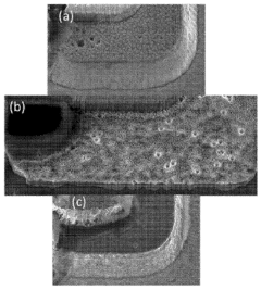
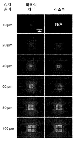
- A manufacturing method involving chemical treatment followed by conformal dielectric deposition, specifically using potassium hydroxide (KOH) treatment and atomic layer deposition (ALD) sidewall passivation, to remove sidewall damage and reduce leakage current, resulting in uniform light emission and improved efficiency.

Micro-led including optimized passivation layer and fabricating method thereof
PatentActiveKR1020210155127A
Innovation
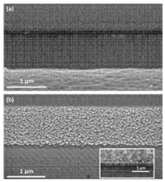
- A micro LED with a double passivation layer formed using a combination of atomic layer deposition (ALD) and plasma-enhanced chemical vapor deposition (PECVD) methods, comprising a first passivation layer of 20-50 nm thickness and a second passivation layer of 250-280 nm thickness, made of dielectric materials like Al2O3, SiO2, SiNx, SiONe, ZrO2, or HfO2, to effectively passivate the sidewalls.


Manufacturing Standards for Micro LED Quality Control
Manufacturing standards for Micro LED quality control represent a critical framework for ensuring consistent performance and reliability in addressing leakage current suppression across backplane sub-pixels. These standards encompass comprehensive testing protocols, measurement methodologies, and acceptance criteria specifically designed to validate the electrical integrity of individual sub-pixel units within the array structure.
The establishment of standardized testing procedures begins with substrate preparation and material qualification protocols. Manufacturing standards mandate rigorous inspection of semiconductor wafer quality, surface roughness parameters, and contamination levels that directly impact leakage current characteristics. Substrate cleaning procedures must adhere to specific chemical treatment sequences and environmental controls to minimize ionic contamination that could contribute to unwanted current pathways.
Electrical characterization standards define precise measurement conditions for leakage current assessment across different operational states. These protocols specify temperature ranges, voltage sweep parameters, and measurement duration requirements to ensure reproducible results. Standards typically require leakage current measurements at multiple bias conditions, including reverse bias stress testing and forward bias threshold evaluations, with acceptance criteria often set below 1 pA per sub-pixel under standard operating conditions.
Process control standards establish critical parameter monitoring throughout the manufacturing sequence. Key control points include ion implantation dose uniformity, annealing temperature profiles, and passivation layer thickness variations. Statistical process control methodologies are implemented to track parameter drift and identify systematic variations that could compromise leakage current performance across production batches.
Quality assurance frameworks incorporate both inline monitoring and final product validation stages. Inline testing standards require real-time electrical parameter monitoring during critical process steps, enabling immediate corrective actions when deviations occur. Final validation protocols mandate comprehensive array-level testing, including pixel-to-pixel uniformity assessments and long-term reliability stress testing under accelerated aging conditions.
Traceability requirements ensure complete documentation of manufacturing parameters and test results for each production lot. These standards facilitate rapid identification of process-related issues and enable continuous improvement initiatives based on statistical analysis of quality metrics and field performance data.
Thermal Management Strategies for Micro LED Arrays
Effective thermal management represents a critical engineering challenge in micro LED arrays, particularly when addressing leakage current suppression across backplane sub-pixels. The miniaturized nature of micro LED devices creates concentrated heat generation zones that can significantly impact electrical performance and reliability. As pixel densities increase and device dimensions shrink below 50 micrometers, thermal effects become increasingly pronounced, directly influencing leakage current characteristics and overall display quality.
Heat dissipation strategies must account for the unique thermal properties of micro LED structures, where localized hotspots can reach temperatures exceeding 85°C during normal operation. These elevated temperatures exacerbate leakage current issues by increasing carrier mobility and reducing barrier heights in semiconductor junctions. Advanced thermal interface materials, including graphene-based composites and phase-change materials, offer promising solutions for efficient heat extraction from individual sub-pixels while maintaining electrical isolation.
Substrate-level thermal management approaches focus on optimizing heat spreading through engineered backplane designs. Silicon carbide and aluminum nitride substrates demonstrate superior thermal conductivity compared to traditional silicon, enabling more effective heat distribution across the array. Micro-channel cooling systems integrated within the backplane structure provide active thermal regulation, though implementation complexity increases significantly with higher pixel densities.
Thermal modeling and simulation tools have become essential for predicting temperature distributions and optimizing cooling strategies. Finite element analysis reveals that thermal crosstalk between adjacent pixels can create temperature gradients exceeding 20°C across small array sections, necessitating sophisticated thermal isolation techniques. Advanced packaging solutions incorporating micro-fins, thermal vias, and embedded cooling channels address these challenges while maintaining manufacturing feasibility.
Emerging thermal management technologies include thermoelectric cooling elements integrated at the sub-pixel level and advanced heat pipe configurations designed specifically for micro LED applications. These innovations target the fundamental relationship between temperature control and leakage current suppression, enabling next-generation display technologies with improved efficiency and longevity.
Unlock deeper insights with Patsnap Eureka Quick Research — get a full tech report to explore trends and direct your research. Try now!
Generate Your Research Report Instantly with AI Agent
Supercharge your innovation with Patsnap Eureka AI Agent Platform!