

Simulating Light Leakage Control in Transparent Micro LED Backplane Structures
JUN 23, 20269 MIN READ
Generate Your Research Report Instantly with AI Agent
Patsnap Eureka helps you evaluate technical feasibility & market potential.
Transparent Micro LED Backplane Development Background and Objectives
The evolution of display technology has witnessed a paradigm shift from traditional liquid crystal displays to advanced micro LED systems, driven by the relentless pursuit of superior visual performance and energy efficiency. Transparent micro LED backplanes represent a revolutionary advancement in this trajectory, offering unprecedented opportunities for next-generation display applications including augmented reality devices, automotive head-up displays, and transparent digital signage systems.
The development of transparent micro LED backplanes emerged from the convergence of semiconductor miniaturization technologies and advanced materials science. Early research in the 2010s focused on conventional micro LED arrays, but the industry quickly recognized the transformative potential of transparent substrates. This technological evolution was catalyzed by breakthroughs in transparent conducting materials, advanced lithography techniques, and precision manufacturing processes that enabled the creation of virtually invisible electronic circuits.
The fundamental challenge in transparent micro LED backplane development lies in achieving optimal light management while maintaining structural transparency. Traditional opaque backplanes provided natural light containment, but transparent architectures introduce complex optical phenomena including unwanted light leakage, internal reflections, and scattering effects. These challenges necessitate sophisticated simulation methodologies to predict and control light behavior within the transparent matrix structure.
Current market demands for immersive display experiences and seamless integration of digital content into physical environments have intensified the focus on transparent display technologies. The automotive industry seeks transparent displays for enhanced driver assistance systems, while retail and architectural applications demand large-scale transparent digital surfaces that blend seamlessly with existing infrastructure.
The primary objective of transparent micro LED backplane development centers on achieving precise light leakage control through advanced simulation techniques. This involves developing comprehensive optical models that accurately predict photon behavior within complex transparent geometries, enabling engineers to optimize pixel isolation, minimize crosstalk, and enhance overall display contrast ratios. Secondary objectives include establishing scalable manufacturing processes, improving long-term reliability under various environmental conditions, and reducing production costs to enable widespread commercial adoption.
Market Demand Analysis for Transparent Display Technologies
The transparent display technology market is experiencing unprecedented growth driven by diverse application sectors seeking innovative visual solutions. Consumer electronics manufacturers are increasingly integrating transparent displays into smartphones, tablets, and wearable devices to create differentiated products with enhanced user experiences. The automotive industry represents a particularly promising segment, where transparent displays enable heads-up displays, smart windshields, and dashboard applications that provide critical information without obstructing driver visibility.
Retail and advertising sectors demonstrate substantial demand for transparent display solutions, utilizing these technologies for storefront windows, product showcases, and interactive advertising installations. Museums, exhibitions, and architectural applications are adopting transparent displays to create immersive experiences while maintaining spatial aesthetics. The healthcare industry shows growing interest in transparent display applications for surgical navigation systems and medical imaging displays.
Current market drivers include the increasing demand for augmented reality applications, smart city infrastructure development, and the growing emphasis on space-efficient display solutions in urban environments. The technology's ability to overlay digital information onto real-world environments addresses the evolving needs of Industry 4.0 applications, including smart manufacturing and logistics visualization systems.
However, market adoption faces significant challenges related to light leakage control, which directly impacts display quality and user acceptance. Poor light management results in reduced contrast ratios, compromised visibility in varying ambient lighting conditions, and overall degraded visual performance. These technical limitations currently restrict widespread commercial deployment and limit market penetration in premium applications.
The demand for improved light leakage control solutions is particularly acute in outdoor applications and high-ambient-light environments where display visibility becomes critical. Professional applications in aviation, marine navigation, and industrial control systems require exceptional display performance standards that current transparent display technologies struggle to meet consistently.
Market research indicates that successful resolution of light leakage challenges could unlock significant growth potential across multiple industry verticals. The convergence of transparent display technology with emerging applications such as smart glass, interactive surfaces, and next-generation user interfaces creates substantial market opportunities for companies developing advanced light management solutions.
Current Challenges in Light Leakage Control for Micro LED Arrays
Light leakage control in micro LED arrays represents one of the most critical technical challenges facing the display industry today. The fundamental issue stems from the inherent optical properties of micro LEDs, where unwanted light emission occurs beyond the intended pixel boundaries, leading to reduced contrast ratios and compromised image quality. This phenomenon becomes particularly pronounced in transparent micro LED backplane structures, where the substrate material itself can act as a light guide, exacerbating cross-talk between adjacent pixels.
The primary challenge lies in the dimensional constraints of micro LED pixels, typically measuring less than 100 micrometers. At these scales, traditional light blocking methods become increasingly ineffective due to manufacturing limitations and the physics of light propagation. Conventional approaches such as black matrix materials face significant hurdles in achieving the precision required for micro-scale applications, while maintaining transparency in the non-emissive areas of the display.
Optical crosstalk presents another substantial obstacle, where light from one pixel interferes with neighboring pixels through various propagation mechanisms. This includes direct lateral emission, substrate-guided modes, and reflection-induced scattering within the transparent backplane structure. The challenge is compounded by the need to maintain high optical efficiency while implementing effective light confinement strategies.
Manufacturing precision requirements pose additional constraints, as current fabrication technologies struggle to achieve the tolerances necessary for effective light leakage control at micro scales. The integration of optical isolation structures must be accomplished without compromising the electrical performance of the underlying thin-film transistor backplane, creating a complex optimization problem between optical and electrical design parameters.
Thermal management issues further complicate light leakage control, as temperature variations can affect both the optical properties of materials and the dimensional stability of micro-scale structures. The transparent nature of the backplane limits the use of traditional thermal dissipation methods, requiring innovative approaches that maintain optical clarity while managing heat generation.
Material compatibility represents a significant technical hurdle, particularly in identifying transparent materials that can provide effective optical isolation while maintaining compatibility with existing semiconductor processing techniques. The challenge extends to developing materials that can withstand the high-temperature processing steps required for micro LED integration while preserving their optical properties over extended operational periods.
Current Light Leakage Simulation and Control Solutions
01 Optical isolation structures and barriers
Implementation of physical barriers and optical isolation structures between micro LED pixels to prevent light leakage and crosstalk. These structures include light-blocking walls, trenches, and isolation layers that confine light emission within designated pixel areas, improving display contrast and preventing unwanted light bleeding between adjacent pixels.- Optical isolation structures and barriers: Implementation of physical barriers and optical isolation structures between micro LED pixels to prevent light leakage and crosstalk. These structures include light-blocking walls, trenches, and isolation layers that confine light emission within designated pixel areas, improving display contrast and preventing unwanted light bleeding between adjacent pixels.
- Transparent electrode and conductive layer optimization: Design and optimization of transparent conductive layers and electrodes in micro LED backplanes to minimize light interference while maintaining electrical functionality. This involves careful selection of materials and layer thicknesses to achieve optimal transparency and conductivity balance, reducing optical losses and unwanted reflections.
- Substrate and backplane material engineering: Development of specialized substrate materials and backplane architectures that enhance transparency while providing structural support for micro LED arrays. This includes the use of advanced transparent materials, optimized layer stacking, and innovative substrate processing techniques to minimize light absorption and scattering.
- Pixel structure and light management design: Optimization of individual pixel structures and light management systems to control light emission direction and minimize stray light. This encompasses pixel geometry optimization, light extraction enhancement features, and directional control elements that improve light efficiency while reducing unwanted light leakage.
- Anti-reflective coatings and surface treatments: Application of specialized coatings and surface treatments to reduce reflections and improve light transmission in transparent micro LED displays. These treatments include anti-reflective layers, surface texturing, and refractive index matching techniques that minimize optical losses and enhance overall display performance.
02 Transparent electrode and conductive layer optimization
Design and optimization of transparent conductive layers and electrodes in micro LED backplanes to minimize light interference while maintaining electrical functionality. This involves careful selection of materials and layer thicknesses to achieve optimal transparency and conductivity balance, reducing optical losses and unwanted reflections.Expand Specific Solutions03 Substrate and backplane material engineering
Development of specialized substrate materials and backplane structures that enhance transparency while providing adequate support for micro LED arrays. This includes the use of advanced transparent materials, optimized layer stacking, and surface treatments to minimize light scattering and absorption within the backplane structure.Expand Specific Solutions04 Pixel architecture and light management
Advanced pixel design strategies that incorporate light management features to control and direct light emission while preventing leakage. This includes optimized pixel geometries, integrated optical elements, and specialized light extraction structures that enhance forward light emission while suppressing lateral light propagation.Expand Specific Solutions05 Anti-reflective coatings and surface treatments
Application of specialized coatings and surface treatments to reduce unwanted reflections and light scattering in transparent micro LED structures. These treatments include anti-reflective layers, index-matching materials, and surface texturing techniques that minimize optical losses and improve overall display performance by reducing stray light and enhancing transparency.Expand Specific Solutions
Major Players in Micro LED and Transparent Display Industry
The transparent micro LED backplane light leakage control technology represents an emerging segment within the rapidly evolving display industry, currently in its early commercialization phase with significant growth potential. The global micro LED market is projected to reach substantial valuations as demand increases for high-performance displays across automotive, AR/VR, and consumer electronics applications. Technology maturity varies considerably among key players, with established display manufacturers like BOE Technology Group, Samsung Display, LG Display, and Sharp Corp. leveraging their extensive TFT-LCD and OLED expertise to advance micro LED solutions. Specialized companies such as VueReal, eLux, and Jade Bird Display are pioneering innovative assembly and manufacturing techniques specifically for micro LED applications. Chinese manufacturers including TCL China Star Optoelectronics and various BOE subsidiaries are aggressively investing in production capabilities, while traditional component suppliers like Alps Alpine and AGC are developing supporting materials and substrates, creating a competitive landscape characterized by both technological innovation and manufacturing scale-up challenges.
BOE Technology Group Co., Ltd.
Technical Solution: BOE Technology has pioneered transparent micro LED backplane structures with integrated light leakage control systems. Their technology employs multi-layered optical films and precision-etched light guides to direct illumination while preventing lateral light bleeding. The company's simulation platform models complex light interactions within transparent substrates, enabling optimization of pixel pitch and backplane thickness. BOE's approach includes developing specialized transparent conductive materials and implementing micro-structured surfaces that enhance light directionality. Their transparent micro LED displays feature advanced compensation algorithms that adjust individual pixel brightness to counteract light leakage effects, achieving superior display uniformity and maintaining transparency levels above 80% in commercial applications.
Strengths include comprehensive manufacturing capabilities and strong simulation expertise. Weaknesses involve challenges in scaling production and material cost optimization.
Sharp Corp.
Technical Solution: Sharp Corporation has established advanced transparent micro LED backplane technologies with sophisticated light leakage control mechanisms. Their approach utilizes precision-engineered optical cavities and anti-reflective coatings to minimize light scattering while maintaining high transparency. The company employs comprehensive simulation tools including Monte Carlo ray-tracing methods to optimize light propagation within transparent substrates and predict leakage patterns. Sharp's technology incorporates specialized barrier structures and wavelength-selective filters that enhance color purity and reduce crosstalk between pixels. Their transparent micro LED systems feature dynamic light management algorithms that adjust emission characteristics based on ambient conditions, achieving transparency levels of approximately 75% while maintaining excellent brightness uniformity and color reproduction accuracy.
Strengths include proven optical engineering expertise and reliable manufacturing quality. Weaknesses involve moderate transparency performance and limited scalability for large displays.
Key Innovations in Optical Simulation for Micro LED Structures
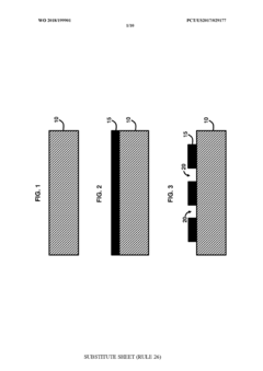
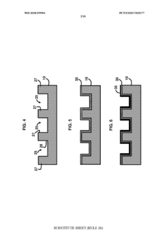
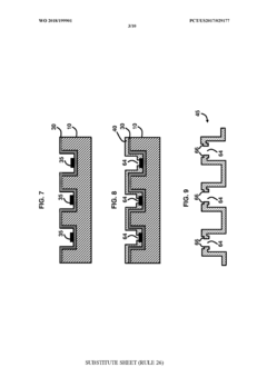
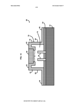
Micro light-emitting diode display with 3D orifice plating and light filtering
PatentWO2018199901A1
Innovation
- A 3D orifice plating with a metal housing and integrated RGB filters is used, where the electroplating process creates a non-transparent metal housing with specific orifices and notches for filters, allowing direct light transmission through translucent filters without refraction, enabling improved light concentration and filtering.
Back emission display
PatentActiveUS11908841B2
Innovation
- A back emission microLED display structure with emission from the back side of a transparent substrate, allowing for fluidic assembly and processing on one side, incorporating reflectors to direct light towards the viewer and simplify the fabrication of microLED displays with all interconnections on one side of the substrate.


Manufacturing Standards for Transparent Electronic Devices
The manufacturing of transparent electronic devices, particularly those incorporating micro LED backplane structures for light leakage control simulation, requires adherence to stringent industry standards that ensure both optical performance and manufacturing consistency. Current manufacturing standards are primarily derived from established display industry protocols, including IEC 62341 series for LED modules and ISO 9241 series for visual display requirements, though these standards require significant adaptation for transparent device applications.
Substrate preparation standards mandate the use of ultra-high transparency materials with light transmission rates exceeding 90% across the visible spectrum. Manufacturing protocols specify surface roughness parameters below 0.5 nm RMS to minimize optical scattering, while maintaining substrate flatness within 2 micrometers across the entire device area. These specifications are critical for accurate light leakage simulation as surface irregularities can introduce unpredictable optical artifacts.
Micro LED fabrication standards emphasize precise dimensional control, with chip placement accuracy requirements of ±1 micrometer and height uniformity within ±0.5 micrometers. The transparent backplane interconnect patterns must maintain line width tolerances of ±10% while ensuring optical transparency is not compromised by conductive traces. Industry standards require the use of materials with refractive indices closely matched to the substrate to minimize optical interference.
Quality control protocols incorporate specialized optical testing procedures beyond conventional electronic device standards. These include spectral transmission measurements across 380-780 nm wavelengths, angular light distribution analysis, and luminance uniformity assessments under various viewing angles. Manufacturing standards specify maximum allowable light leakage levels of less than 0.1% of total luminous output in off-state conditions.
Environmental testing standards for transparent electronic devices extend traditional reliability requirements to include thermal cycling effects on optical properties, humidity resistance testing for transparent encapsulation materials, and long-term stability assessments of optical transmission characteristics. These comprehensive manufacturing standards ensure that transparent micro LED devices maintain both electronic functionality and optical performance throughout their operational lifetime.
Optical Performance Optimization in Micro LED Backplane Design
Optical performance optimization in micro LED backplane design represents a critical engineering challenge that directly impacts display quality, energy efficiency, and manufacturing viability. The primary objective centers on maximizing light extraction efficiency while minimizing unwanted optical phenomena such as crosstalk, color mixing, and luminance non-uniformity across the display surface.
The optimization process encompasses multiple interconnected parameters including pixel pitch, substrate transparency, electrode configuration, and optical isolation structures. Advanced simulation methodologies enable engineers to model complex light propagation behaviors within transparent backplane architectures, accounting for refractive index variations, surface roughness effects, and material absorption characteristics. These computational approaches facilitate the exploration of design spaces that would be prohibitively expensive to investigate through physical prototyping alone.
Key performance metrics driving optimization efforts include luminous efficacy, color gamut coverage, contrast ratio, and angular viewing characteristics. The transparent nature of micro LED backplanes introduces unique optical considerations, particularly regarding substrate-mediated light scattering and reflection losses at material interfaces. Optimization strategies must balance these competing factors while maintaining electrical functionality and thermal management requirements.
Contemporary optimization approaches leverage machine learning algorithms and multi-objective optimization techniques to navigate the complex parameter space efficiently. These methods enable simultaneous consideration of optical, electrical, and thermal constraints, leading to more robust design solutions. Particular attention focuses on minimizing optical crosstalk between adjacent pixels through strategic placement of light-blocking structures and optimization of pixel isolation geometries.
The integration of advanced materials such as quantum dots, photonic crystals, and metamaterial structures offers additional optimization pathways. These materials enable precise control over light emission directionality, spectral characteristics, and polarization properties. However, their incorporation requires careful consideration of manufacturing compatibility and long-term stability under operational conditions.
Emerging optimization frameworks incorporate real-time feedback mechanisms that adapt display characteristics based on content analysis and ambient lighting conditions. This dynamic approach represents a paradigm shift from static optimization toward intelligent, responsive optical systems that continuously maximize performance across varying operational scenarios.
Unlock deeper insights with Patsnap Eureka Quick Research — get a full tech report to explore trends and direct your research. Try now!
Generate Your Research Report Instantly with AI Agent
Supercharge your innovation with Patsnap Eureka AI Agent Platform!