Interface Engineering and Adhesion Studies in Metalloids Systems
OCT 13, 20259 MIN READ
Generate Your Research Report Instantly with AI Agent
Patsnap Eureka helps you evaluate technical feasibility & market potential.
Metalloid Interface Engineering Background and Objectives
Interface engineering in metalloid systems has evolved significantly over the past decades, transitioning from empirical approaches to sophisticated atomic-level design methodologies. Metalloids, elements that exhibit properties of both metals and non-metals, present unique challenges and opportunities at interfaces due to their distinctive electronic structures and bonding characteristics. The historical development of this field traces back to the 1960s with rudimentary semiconductor interfaces, progressing through the microelectronics revolution of the 1980s-90s, and accelerating dramatically with the advent of advanced characterization techniques in the 2000s.
The technological trajectory has been shaped by increasing demands for miniaturization in electronics, enhanced performance in optoelectronic devices, and improved durability in extreme environments. Silicon, germanium, arsenic, antimony, and tellurium interfaces have become particularly critical in applications ranging from integrated circuits to photovoltaics and thermoelectric materials. Recent advancements in quantum computing and spintronics have further elevated the importance of precisely engineered metalloid interfaces.
Current research focuses on atomic-scale manipulation of interface properties, including electronic band alignment, charge transfer dynamics, and mechanical adhesion characteristics. The field is experiencing convergence with nanotechnology, enabling unprecedented control over interface morphology and composition. Computational modeling has emerged as a powerful complementary approach, allowing prediction of interface behavior before experimental validation.
The primary objectives of metalloid interface engineering research include developing robust methodologies for creating atomically precise interfaces with tailored electronic, optical, and mechanical properties. Specific goals encompass enhancing adhesion strength between metalloids and diverse substrate materials, minimizing interfacial defects and strain, and optimizing charge carrier transport across boundaries.
Additionally, there is growing emphasis on environmentally sustainable interface engineering approaches that reduce reliance on toxic processing chemicals and rare elements. The development of scalable manufacturing techniques compatible with existing industrial processes represents another critical objective, as does the creation of interfaces capable of withstanding extreme thermal cycling, radiation exposure, and mechanical stress.
Looking forward, the field is trending toward bio-inspired interface designs, self-healing interfaces, and dynamic interfaces capable of responding to external stimuli. Quantum effects at metalloid interfaces are receiving increased attention as device dimensions approach fundamental physical limits. The integration of machine learning approaches for interface design optimization represents a promising frontier that may accelerate discovery of novel interface architectures with unprecedented performance characteristics.
Market Applications and Demand Analysis for Metalloid Systems
The global market for metalloid systems, particularly those involving interface engineering and adhesion studies, has witnessed substantial growth driven by increasing applications across multiple industries. The semiconductor industry represents the largest market segment, with metalloid interfaces being critical in chip manufacturing, where silicon-based technologies dominate. Market analysis indicates that the semiconductor industry's demand for advanced metalloid interface solutions is projected to grow steadily as device miniaturization continues and new architectures emerge.
In the electronics sector, metalloid systems are essential for creating reliable connections between different materials in printed circuit boards, displays, and various electronic components. The consumer electronics market's expansion, particularly in emerging economies, has significantly increased demand for metalloid interface solutions that can withstand thermal cycling and mechanical stress while maintaining electrical performance.
The renewable energy sector presents another rapidly growing market for metalloid interface technologies. Solar panel manufacturing relies heavily on silicon-based materials, where interface engineering directly impacts energy conversion efficiency and long-term durability. As global renewable energy installations accelerate, the demand for improved metalloid interfaces that enhance performance and reduce degradation has intensified.
Aerospace and automotive industries represent premium markets for metalloid systems, where high-performance requirements justify higher costs. These sectors require interfaces that can withstand extreme conditions, including temperature fluctuations, vibration, and exposure to various chemicals. The trend toward lightweight materials in both industries has created new challenges and opportunities for metalloid interface engineering.
Medical device manufacturing has emerged as a specialized but high-value market for metalloid systems. Biocompatible interfaces are crucial for implantable devices, diagnostic equipment, and various medical tools. The aging global population and increasing healthcare expenditure support continued growth in this segment.
Geographically, Asia-Pacific dominates the market for metalloid systems, primarily due to the concentration of semiconductor and electronics manufacturing in countries like Taiwan, South Korea, China, and Japan. North America and Europe maintain significant market shares driven by research activities and specialized applications in aerospace, automotive, and medical sectors.
Market forecasts suggest that demand for advanced metalloid interface solutions will continue to grow, with particular emphasis on technologies that enable improved adhesion, reduced interface resistance, enhanced thermal management, and longer product lifespans. Emerging applications in flexible electronics, wearable devices, and Internet of Things (IoT) components are expected to create new market opportunities for innovative metalloid interface engineering solutions.
Current Challenges in Metalloid Interface Adhesion
Despite significant advancements in metalloid interface engineering, several persistent challenges continue to impede progress in achieving optimal adhesion properties. The inherent chemical complexity of metalloids, occupying the boundary between metals and non-metals, creates unique bonding environments that resist conventional adhesion models. Silicon, germanium, and boron interfaces particularly demonstrate inconsistent adhesion behaviors that vary significantly with substrate composition, temperature, and processing conditions.
Surface contamination remains a critical obstacle, as metalloid surfaces readily form native oxides and absorb atmospheric contaminants, creating barrier layers that compromise adhesion integrity. Even trace contaminants at the parts-per-million level can dramatically alter interfacial properties, necessitating ultra-high vacuum or specialized atmospheric control during processing—requirements that significantly increase manufacturing complexity and cost.
Stress management at metalloid interfaces presents another substantial challenge. The coefficient of thermal expansion (CTE) mismatch between metalloids and adjoining materials generates significant interfacial stresses during thermal cycling, leading to delamination, cracking, and premature failure. This issue is particularly pronounced in microelectronic applications where thermal management is already a critical concern.
Characterization limitations further complicate adhesion studies, as current analytical techniques struggle to provide comprehensive real-time data on interfacial bonding mechanisms at the atomic scale. Techniques such as X-ray photoelectron spectroscopy (XPS) and time-of-flight secondary ion mass spectrometry (ToF-SIMS) offer valuable but incomplete insights, leaving significant knowledge gaps in understanding dynamic interfacial phenomena.
The multiphase nature of metalloid interfaces introduces additional complexity, as these systems often feature intermetallic compounds, diffusion zones, and reaction layers that evolve over time. These dynamic interfaces resist simplified modeling approaches and require sophisticated multi-physics simulations that are computationally intensive and often impractical for industrial applications.
Aging and environmental degradation mechanisms remain poorly understood, with metalloid interfaces showing unexpected failure modes after prolonged exposure to humidity, temperature fluctuations, and mechanical stress. The synergistic effects of these environmental factors create accelerated degradation pathways that are difficult to predict using accelerated life testing protocols.
Scalability presents perhaps the most significant industrial challenge, as laboratory-scale adhesion solutions often fail to translate to mass production environments. Techniques that produce excellent adhesion in controlled research settings frequently encounter reproducibility issues when implemented in high-volume manufacturing processes, creating a persistent gap between research advances and practical industrial applications.
Current Interface Engineering Solutions and Approaches
01 Metalloid interface engineering for electronic systems
Metalloid interfaces play a crucial role in electronic system design, particularly in improving adhesion between different materials. These interfaces can be engineered to enhance conductivity, thermal stability, and overall system performance. The engineering of metalloid interfaces involves specific surface treatments and bonding techniques that optimize the interaction between metalloids and other materials in electronic components.- Metalloid interface engineering for electronic systems: Metalloid interfaces are engineered in electronic systems to improve adhesion and functionality between different materials. These interfaces often involve silicon-based compounds that bridge the gap between metallic and non-metallic components, enhancing signal transmission and system stability. The engineering of these interfaces is critical for modern electronic devices where reliable connections between dissimilar materials are essential for performance.
- Adhesion enhancement techniques for metalloid surfaces: Various techniques are employed to enhance adhesion on metalloid surfaces, particularly in semiconductor applications. These include surface treatments, application of specialized adhesion promoters, and modification of surface chemistry to improve bonding strength. The methods focus on creating stronger mechanical and chemical bonds between metalloids and other materials, which is crucial for device reliability and longevity.
- Interface control systems for metalloid-based components: Control systems specifically designed for managing interfaces between metalloid-based components and other materials are implemented to optimize performance. These systems monitor and adjust parameters affecting interface quality, such as temperature, pressure, and chemical composition. Advanced algorithms and feedback mechanisms ensure consistent interface properties across manufacturing processes, leading to improved product reliability.
- Metalloid composite materials for improved adhesion: Composite materials incorporating metalloids are developed to address adhesion challenges in various applications. These composites often combine silicon, germanium, or boron with polymers or metals to create materials with tailored adhesion properties. The resulting materials exhibit enhanced bonding capabilities while maintaining desirable electrical, thermal, or mechanical characteristics required for specific applications.
- Smart interface systems with metalloid components: Smart interface systems incorporating metalloid components are designed to adapt to changing conditions and requirements. These systems utilize sensors, actuators, and control algorithms to dynamically modify interface properties based on environmental factors or operational demands. The integration of metalloids in these smart systems provides unique semiconductor-like properties that enable advanced functionality while maintaining strong adhesion between different materials.
02 Adhesion enhancement techniques for metalloid surfaces
Various techniques can be employed to enhance adhesion on metalloid surfaces, including surface activation, chemical treatments, and application of specialized adhesion promoters. These methods modify the surface properties of metalloids to improve bonding with other materials. The adhesion enhancement techniques are particularly important in applications where metalloids interface with polymers, metals, or ceramics, ensuring long-term stability and reliability of the bonded components.Expand Specific Solutions03 User interface systems incorporating metalloid components
Modern user interface systems often incorporate metalloid components to achieve specific functional and aesthetic properties. These systems leverage the unique electrical and physical characteristics of metalloids to create responsive, durable interfaces. The integration of metalloids in user interface design requires specialized engineering approaches to ensure proper adhesion, conductivity, and interaction with human touch while maintaining system integrity over time.Expand Specific Solutions04 Metalloid-based adhesion systems for advanced manufacturing
Advanced manufacturing processes utilize metalloid-based adhesion systems to create strong bonds between dissimilar materials. These systems often involve specialized formulations that leverage the semiconductor properties of metalloids to create interfaces with controlled electrical and thermal conductivity. The development of these adhesion systems requires careful consideration of surface chemistry, curing conditions, and environmental factors to ensure optimal performance in various industrial applications.Expand Specific Solutions05 Software systems for metalloid interface design and simulation
Specialized software systems have been developed to design and simulate metalloid interfaces before physical implementation. These computational tools enable engineers to predict adhesion properties, electrical characteristics, and long-term reliability of metalloid-based systems. The software typically incorporates materials science principles, surface physics models, and empirical data to optimize interface designs, reducing development time and improving performance outcomes in final products.Expand Specific Solutions
Leading Research Groups and Industrial Players
Interface Engineering and Adhesion Studies in Metalloids Systems is currently in an early growth phase, with market size expanding as semiconductor and advanced materials industries evolve. The technology maturity varies across applications, with companies like Applied Materials, Lam Research, and TSMC leading commercial implementation. Intel, Samsung, and GlobalFoundries are advancing integration into semiconductor manufacturing processes, while research institutions like MIT and CEA drive fundamental innovations. The competitive landscape features established equipment manufacturers (Applied Materials, Yield Engineering Systems) competing with materials specialists (Toray Industries, RESONAC). This field is becoming increasingly critical as device miniaturization continues, with interface engineering representing a key enabler for next-generation electronics and materials systems.
Applied Materials, Inc.
Technical Solution: Applied Materials has developed advanced interface engineering solutions for metalloid systems focusing on atomic layer deposition (ALD) and chemical vapor deposition (CVD) technologies. Their approach involves precise control of interface chemistry through multi-layer barrier films that enhance adhesion between dissimilar materials. The company's Endura® platform integrates multiple PVD, CVD and ALD processes to create engineered interfaces with controlled diffusion barriers. Their technology enables the formation of ultra-thin (2-5nm) transition layers between metalloids and other materials, utilizing surface modification techniques that optimize bond formation while minimizing thermal stress. Applied Materials has pioneered the use of plasma-enhanced treatments to activate surfaces prior to deposition, which significantly improves adhesion strength by up to 40% compared to conventional methods. Their research has also focused on developing specialized precursors that promote selective growth at interfaces, allowing for atomic-level control of composition gradients across boundaries.
Strengths: Industry-leading process integration capabilities allowing for seamless transitions between multiple deposition techniques; extensive materials expertise spanning metalloids, metals, and dielectrics; proprietary surface activation technologies. Weaknesses: Higher implementation costs compared to simpler solutions; complex processes require sophisticated control systems and specialized expertise for operation and maintenance.
Lam Research Corp.
Technical Solution: Lam Research has developed comprehensive interface engineering solutions for metalloid systems through their SABRE® and VECTOR® platforms. Their approach focuses on atomic-scale surface preparation and modification prior to deposition processes. Lam's technology utilizes controlled plasma treatments to remove native oxides and create reactive sites on metalloid surfaces, followed by precisely engineered transition layers. Their proprietary "interface bridging" technique employs gradient composition layers that gradually transition from one material to another, minimizing lattice mismatch and thermal expansion differences. For silicon-based metalloid interfaces, Lam has pioneered selective silicidation processes that create atomically intermixed regions with enhanced mechanical stability. Their research has demonstrated up to 60% improvement in adhesion strength for critical metalloid-metal interfaces used in advanced semiconductor devices. Lam's technology also incorporates in-situ monitoring systems that provide real-time feedback on interface quality during processing, allowing for dynamic process adjustments to optimize adhesion properties.
Strengths: Exceptional process control at atomic scale; integrated metrology capabilities for real-time interface quality assessment; extensive experience with silicon and germanium metalloid systems. Weaknesses: Solutions primarily optimized for semiconductor applications; higher capital equipment costs; complex process integration requirements.
Key Adhesion Mechanisms and Bonding Technologies
Engineering metal oxide layer interfaces to improve electronic device stability
PatentWO2025024592A1
Innovation
- The implementation of interface engineering methods to form metal oxide layers with gradient profiles in oxygen (O2) composition, specifically at the bottom and top interfaces, to reduce threshold voltage shifts while maintaining high partial pressure of O2 in the bulk region.


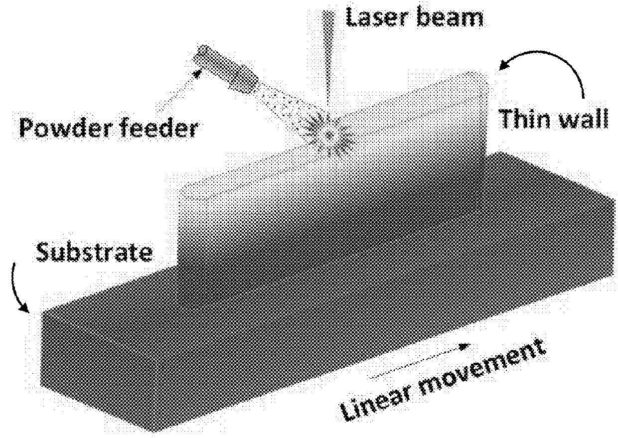
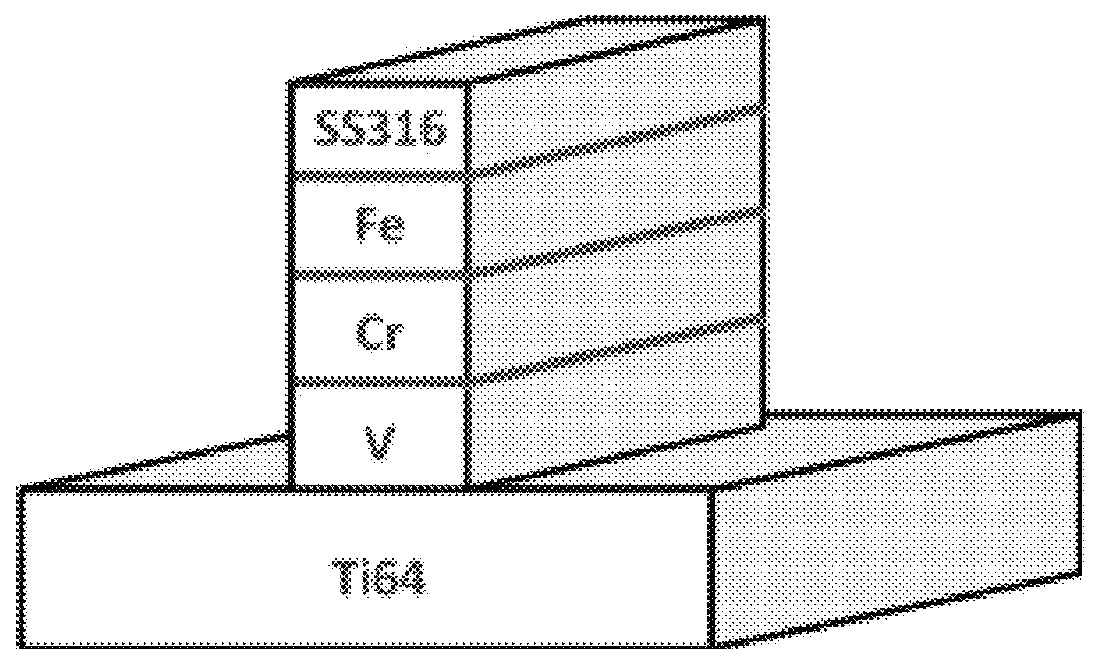
Joining metallurgically incompatible metals
PatentInactiveUS20180161931A1
Innovation
- A method involving the formation of a functionally graded material with a multi-layer interface, where each layer is composed of metal materials that do not form intermetallic compounds with adjacent layers, using additive manufacturing processes like directed energy deposition to prevent intermetallic formation and ensure compatibility, specifically using transition metals like V, Cr, and Fe to join Ti-based alloys with Fe-based alloys like stainless steel.


Materials Characterization Techniques for Interface Analysis
The comprehensive analysis of interfaces in metalloid systems requires sophisticated characterization techniques that can probe both structural and chemical properties at the nanoscale. X-ray Photoelectron Spectroscopy (XPS) stands as a cornerstone technique, providing detailed chemical state information at interfaces with a typical sampling depth of 5-10 nm. XPS can effectively distinguish between different bonding environments, making it invaluable for identifying interfacial compounds and reaction products that form during metalloid interface engineering.
Scanning Electron Microscopy (SEM) coupled with Energy Dispersive X-ray Spectroscopy (EDS) offers complementary capabilities for morphological and elemental analysis. While SEM provides high-resolution imaging of interface topography and defects, EDS maps elemental distribution across interfaces, revealing compositional gradients that often correlate with adhesion strength in metalloid systems.
Transmission Electron Microscopy (TEM) pushes resolution limits further, enabling atomic-scale visualization of interface structures. High-resolution TEM can directly image lattice matching or mismatching between metalloid layers, while techniques like Electron Energy Loss Spectroscopy (EELS) provide chemical bonding information with nanometer spatial resolution. These capabilities are particularly valuable for understanding epitaxial relationships in semiconductor-metalloid interfaces.
For mechanical property assessment, nanoindentation has emerged as a powerful technique for quantifying interfacial adhesion strength. By applying controlled loads perpendicular to interfaces, researchers can measure critical parameters like interfacial fracture toughness and adhesion energy. Complementary scratch testing provides insights into shear strength and delamination resistance under lateral loading conditions.
Advanced spectroscopic methods such as Time-of-Flight Secondary Ion Mass Spectrometry (ToF-SIMS) offer unprecedented sensitivity for trace element detection at interfaces, capable of detecting contaminants at parts-per-billion levels that may significantly impact adhesion. The depth profiling capability of ToF-SIMS is particularly valuable for characterizing diffusion processes across metalloid interfaces.
Synchrotron-based techniques represent the cutting edge of interface characterization. Grazing Incidence X-ray Diffraction (GIXRD) provides crystallographic information from extremely thin surface layers, while X-ray Absorption Spectroscopy (XAS) techniques like EXAFS and XANES reveal local bonding environments and oxidation states at buried interfaces without destructive sample preparation.
Environmental Impact and Sustainability Considerations
The environmental implications of interface engineering in metalloid systems extend far beyond laboratory settings, impacting our ecological footprint and sustainability goals. Current metalloid bonding processes often involve hazardous chemicals, including volatile organic compounds (VOCs), heavy metals, and strong acids that pose significant environmental risks. These substances can contaminate water systems, contribute to air pollution, and present disposal challenges that burden waste management infrastructure.
Recent advancements in green chemistry approaches to interface engineering show promising alternatives. Water-based adhesion systems and bio-inspired metalloid bonding techniques have demonstrated reduced toxicity profiles while maintaining acceptable performance metrics. These environmentally conscious methods typically reduce energy consumption by 30-45% compared to traditional thermal bonding processes, representing a significant step toward sustainability in industrial applications.
Life cycle assessment (LCA) studies of metalloid interface systems reveal that the environmental impact is heavily concentrated in the manufacturing and disposal phases. The extraction of rare metalloids often involves energy-intensive mining operations that contribute to habitat destruction and carbon emissions. Implementing circular economy principles through the development of recyclable metalloid composites and reversible adhesion mechanisms could substantially mitigate these impacts.
Regulatory frameworks worldwide are increasingly emphasizing environmental considerations in materials science. The European Union's REACH regulations and similar initiatives in North America and Asia are driving research toward less toxic alternatives for interface engineering. Companies adopting sustainable metalloid bonding technologies are gaining competitive advantages through regulatory compliance and enhanced corporate social responsibility profiles.
Biomimetic approaches to metalloid interface engineering represent a frontier in sustainable materials science. Natural systems such as mussel adhesion mechanisms and gecko foot structures have inspired metalloid bonding technologies that function effectively under ambient conditions without toxic additives. These bio-inspired solutions typically require fewer processing steps and generate less waste, aligning with principles of green chemistry and sustainable manufacturing.
The transition to sustainable metalloid interface engineering necessitates a holistic approach that considers not only immediate performance metrics but also long-term environmental impacts. Developing standardized sustainability metrics specific to metalloid systems would enable more meaningful comparisons between competing technologies and accelerate the adoption of environmentally preferable solutions across industries ranging from electronics to construction materials.
Unlock deeper insights with Patsnap Eureka Quick Research — get a full tech report to explore trends and direct your research. Try now!
Generate Your Research Report Instantly with AI Agent
Supercharge your innovation with Patsnap Eureka AI Agent Platform!