

MicroLED backplanes vs monolithic: which lowers defect density per cm²?
MAY 7, 20269 MIN READ
Generate Your Research Report Instantly with AI Agent
PatSnap Eureka helps you evaluate technical feasibility & market potential.
MicroLED Backplane Technology Background and Objectives
MicroLED technology represents a revolutionary advancement in display manufacturing, emerging as a next-generation solution that combines the benefits of organic light-emitting diodes (OLEDs) with enhanced durability, brightness, and energy efficiency. This technology utilizes microscopic LEDs, typically measuring less than 100 micrometers, to create individual pixels that emit light directly without requiring backlighting systems. The evolution from traditional LCD and OLED displays to MicroLED has been driven by increasing demands for higher resolution, improved color accuracy, and extended operational lifespans in applications ranging from consumer electronics to industrial displays.
The fundamental challenge in MicroLED manufacturing lies in achieving acceptable defect density levels while maintaining cost-effective production scalability. Defect density, measured in defects per square centimeter, directly impacts display quality, manufacturing yield, and overall commercial viability. Current industry standards require defect densities below 10^-4 defects per cm² for consumer applications, with even stricter requirements for premium displays.
Two primary technological approaches have emerged to address manufacturing challenges: backplane-based architectures and monolithic integration methods. Backplane technology involves fabricating MicroLED chips separately and subsequently transferring them onto prepared substrates containing driving circuitry. This approach allows for independent optimization of LED performance and driving electronics, potentially enabling better defect management through selective placement and testing procedures.
Monolithic integration represents an alternative strategy where MicroLEDs are grown directly on substrates containing integrated driving circuits. This approach eliminates mass transfer processes, potentially reducing handling-related defects while enabling tighter integration between optical and electronic components. However, monolithic methods face constraints related to substrate compatibility and thermal processing limitations.
The primary objective of this technological investigation centers on determining which approach delivers superior defect density performance per unit area. This evaluation encompasses analyzing manufacturing process variations, yield optimization strategies, and scalability considerations that influence overall defect rates. Understanding these factors is crucial for establishing viable commercial production pathways and meeting increasingly stringent quality requirements in next-generation display applications.
Secondary objectives include identifying specific defect mechanisms inherent to each approach, evaluating repair and redundancy strategies, and assessing long-term reliability implications that affect sustained performance in deployed systems.
Market Demand Analysis for Low-Defect MicroLED Displays
The global display industry is experiencing unprecedented demand for high-performance, low-defect MicroLED displays across multiple application segments. Consumer electronics manufacturers are increasingly prioritizing display technologies that offer superior brightness, energy efficiency, and reliability, driving substantial market interest in MicroLED solutions with minimal defect densities.
Premium smartphone manufacturers represent a critical market segment demanding ultra-low defect MicroLED displays. These devices require pixel-perfect visual quality for competitive differentiation, making defect density a paramount concern. The transition from OLED to MicroLED technology in flagship devices depends heavily on achieving defect rates comparable to or better than existing display technologies.
The automotive industry presents another significant demand driver for low-defect MicroLED displays. Advanced driver assistance systems, heads-up displays, and in-vehicle infotainment systems require exceptional reliability and longevity. Automotive applications particularly value the superior outdoor visibility and temperature stability that MicroLED technology provides, but only when defect rates meet stringent automotive quality standards.
Augmented reality and virtual reality applications constitute rapidly expanding market segments with stringent defect tolerance requirements. These applications demand extremely high pixel densities and uniform brightness across the display surface. Even minor defects become highly visible and disruptive to user experience, creating strong market demand for manufacturing approaches that minimize defect occurrence.
Large-scale display applications, including digital signage and broadcast displays, represent substantial market opportunities for low-defect MicroLED technology. These applications require seamless visual experiences across expansive display surfaces, where defects become magnified and commercially unacceptable. The modular nature of many large-scale installations makes defect management particularly challenging and economically significant.
Wearable device manufacturers increasingly seek MicroLED displays that combine compact form factors with exceptional reliability. Smartwatches, fitness trackers, and emerging wearable categories demand displays that maintain consistent performance throughout extended operational periods. The small display sizes in wearables make individual pixel defects proportionally more impactful on overall visual quality.
The medical device sector presents specialized demand for ultra-reliable MicroLED displays in surgical equipment, diagnostic devices, and patient monitoring systems. These applications require displays with minimal failure rates and consistent performance under demanding operational conditions, creating premium market segments willing to invest in superior defect management approaches.
Market research indicates that display manufacturers are actively evaluating both backplane and monolithic MicroLED approaches based primarily on their respective defect density characteristics. The manufacturing approach that demonstrates superior defect management capabilities will likely capture dominant market share across these diverse application segments.
Current Defect Density Challenges in MicroLED Manufacturing
MicroLED manufacturing faces unprecedented defect density challenges that significantly impact yield rates and commercial viability. Current industry data indicates defect densities ranging from 10^3 to 10^5 defects per cm², far exceeding the stringent requirements for high-resolution display applications. These defect levels translate to yield rates below 50% for large-area displays, creating substantial cost barriers for mass production.
The primary defect categories plaguing MicroLED manufacturing include dead pixels, stuck pixels, wavelength variations, and luminance non-uniformity. Dead pixels, caused by complete LED failure or electrical disconnection, represent the most critical defect type as they are immediately visible to end users. Industry standards typically require less than 1 dead pixel per million for premium display applications, yet current manufacturing processes struggle to achieve this specification consistently across large substrates.
Wavelength uniformity presents another significant challenge, with acceptable color variations requiring wavelength control within ±2-3 nanometers across the entire display area. Current manufacturing processes exhibit wavelength variations of ±10-15 nanometers, necessitating complex binning and sorting procedures that further reduce effective yield rates. This wavelength inconsistency stems from epitaxial growth variations, thermal processing differences, and substrate-induced stress variations during fabrication.
Luminance uniformity defects manifest as brightness variations across the display surface, typically requiring uniformity better than 95% for acceptable visual performance. Current processes achieve uniformity levels of 80-90%, with variations attributed to mesa etching inconsistencies, contact resistance variations, and thermal management challenges during operation.
The manufacturing yield crisis becomes particularly acute when scaling to larger display sizes. While 1-inch diagonal displays might achieve 70-80% yield rates, scaling to 10-inch displays reduces yields to below 20% due to the multiplicative nature of defect probability across larger areas. This scaling challenge represents the fundamental barrier preventing MicroLED technology from competing effectively with established display technologies in large-format applications.
Process-induced defects during mass transfer operations contribute significantly to overall defect density. Pick-and-place accuracy limitations, adhesive contamination, and mechanical stress during transfer create additional failure modes that compound epitaxial and processing defects. Current mass transfer processes exhibit placement accuracy of ±2-5 micrometers, while optimal performance requires sub-micrometer precision for high-density pixel arrays.
Current Solutions for MicroLED Defect Density Reduction
01 MicroLED defect detection and inspection methods
Various optical and electrical inspection techniques are employed to identify and quantify defects in microLED arrays. These methods include automated optical inspection systems, electrical testing protocols, and advanced imaging techniques that can detect pixel defects, brightness variations, and structural anomalies at the microscale level. The detection methods are crucial for quality control and yield improvement in manufacturing processes.- MicroLED defect detection and inspection methods: Various optical and electrical inspection techniques are employed to identify and quantify defects in microLED arrays. These methods include automated optical inspection systems, electroluminescence testing, and advanced imaging techniques that can detect pixel-level defects, dark spots, and brightness non-uniformities. The detection systems utilize high-resolution cameras and specialized algorithms to analyze the performance characteristics of individual microLED pixels.
- Manufacturing process optimization to reduce defect density: Defect density in microLED devices can be significantly reduced through optimized manufacturing processes including improved epitaxial growth conditions, enhanced lithography techniques, and controlled etching processes. Process parameters such as temperature control, material purity, and clean room environments are critical factors in minimizing structural defects and ensuring uniform device characteristics across large arrays.
- Repair and compensation techniques for defective pixels: Advanced repair methodologies are developed to address defective pixels in microLED displays, including laser repair techniques, redundant pixel architectures, and electrical compensation circuits. These approaches can restore functionality to defective areas or provide alternative current paths to maintain display uniformity and extend device lifetime despite the presence of some defective elements.
- Statistical analysis and modeling of defect distribution: Comprehensive statistical models are employed to analyze defect patterns and predict failure rates in microLED arrays. These models help establish quality control standards, yield prediction algorithms, and reliability assessment frameworks. The analysis includes spatial distribution mapping, temporal degradation studies, and correlation analysis between manufacturing parameters and defect occurrence rates.
- Material engineering approaches for defect mitigation: Advanced material engineering strategies focus on reducing intrinsic defect formation through improved substrate preparation, buffer layer optimization, and quantum well structure design. These approaches target the fundamental sources of defects such as threading dislocations, point defects, and interface irregularities that can impact the electrical and optical performance of microLED devices.
02 Manufacturing process optimization to reduce defect density
Optimization of fabrication processes including epitaxial growth, lithography, etching, and transfer techniques to minimize defect formation during microLED production. Process parameters such as temperature control, material purity, and environmental conditions are carefully managed to reduce structural defects, contamination, and yield loss. Advanced manufacturing techniques focus on improving uniformity and reducing variability across large-area substrates.Expand Specific Solutions03 Defect classification and characterization systems
Systematic approaches to categorize and analyze different types of defects found in microLED devices, including dead pixels, brightness non-uniformity, color shift, and electrical failures. These systems utilize machine learning algorithms and statistical analysis to identify defect patterns, root causes, and correlations with manufacturing parameters. The classification helps in developing targeted solutions for specific defect types.Expand Specific Solutions04 Repair and compensation techniques for defective pixels
Methods to address defective pixels in microLED displays through redundancy schemes, pixel replacement, laser repair, and electrical compensation. These techniques include spare pixel activation, current redistribution, and optical correction methods to maintain display quality despite the presence of defective elements. Advanced repair strategies can significantly improve effective yield and display performance.Expand Specific Solutions05 Quality control standards and yield enhancement strategies
Establishment of quality metrics, acceptance criteria, and statistical process control methods specifically designed for microLED manufacturing. These strategies encompass defect density thresholds, reliability testing protocols, and continuous improvement methodologies. The approaches focus on achieving commercial viability through systematic yield enhancement and cost reduction while maintaining acceptable quality levels for different application requirements.Expand Specific Solutions
Key Players in MicroLED Backplane and Monolithic Technologies
The MicroLED industry is in its early commercialization phase, transitioning from R&D to limited production, with the market expected to reach significant scale by 2030. The competitive landscape reveals a multi-billion dollar opportunity driven by demand for high-resolution displays across consumer electronics, automotive, and AR/VR applications. Technology maturity varies significantly among key players: established display manufacturers like BOE Technology Group, TCL China Star, and Sharp Corp. leverage existing infrastructure for backplane development, while specialized companies such as VueReal focus on innovative microSolid printing platforms. Chinese companies including Chengdu Vistar Optoelectronics and BOE Mled Technology are advancing TFT-based micro-LED solutions, competing with international players like Seoul Viosys and SmartKem. The defect density challenge remains critical, with both backplane and monolithic approaches showing promise depending on application requirements and manufacturing capabilities.
BOE Technology Group Co., Ltd.
Technical Solution: BOE has developed advanced MicroLED backplane technologies focusing on LTPS (Low Temperature Poly-Silicon) and oxide TFT backplanes for MicroLED displays. Their approach emphasizes hybrid integration methods that combine the benefits of both backplane and monolithic approaches. BOE's technology utilizes mass transfer techniques with improved yield rates and has developed proprietary defect detection and repair mechanisms during the manufacturing process. The company has invested heavily in reducing pixel pitch while maintaining high aperture ratios, achieving defect densities below 10 ppm through advanced process control and real-time monitoring systems.
Strengths: Mature manufacturing infrastructure, advanced mass transfer technology, strong defect detection capabilities. Weaknesses: Higher manufacturing complexity, significant capital investment requirements for hybrid approaches.
Mitsubishi Electric Corp.
Technical Solution: Mitsubishi Electric has developed MicroLED technologies focusing on hybrid backplane approaches that combine the advantages of both discrete and monolithic methods. Their technology emphasizes advanced bonding techniques and thermal management solutions to reduce stress-induced defects during manufacturing and operation. Mitsubishi's approach incorporates sophisticated yield enhancement strategies including selective binning and adaptive compensation circuits. The company has implemented advanced metrology systems for defect detection and has developed proprietary repair techniques that can address defects post-manufacturing. Their technology demonstrates improved reliability and reduced defect density through comprehensive quality control measures.
Strengths: Strong reliability engineering, advanced bonding technologies, comprehensive quality control systems. Weaknesses: Conservative approach may limit innovation speed, higher manufacturing complexity for hybrid solutions.
Core Innovations in Backplane vs Monolithic Architectures
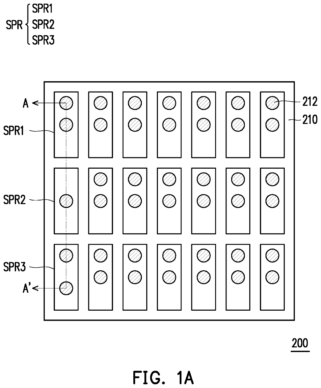
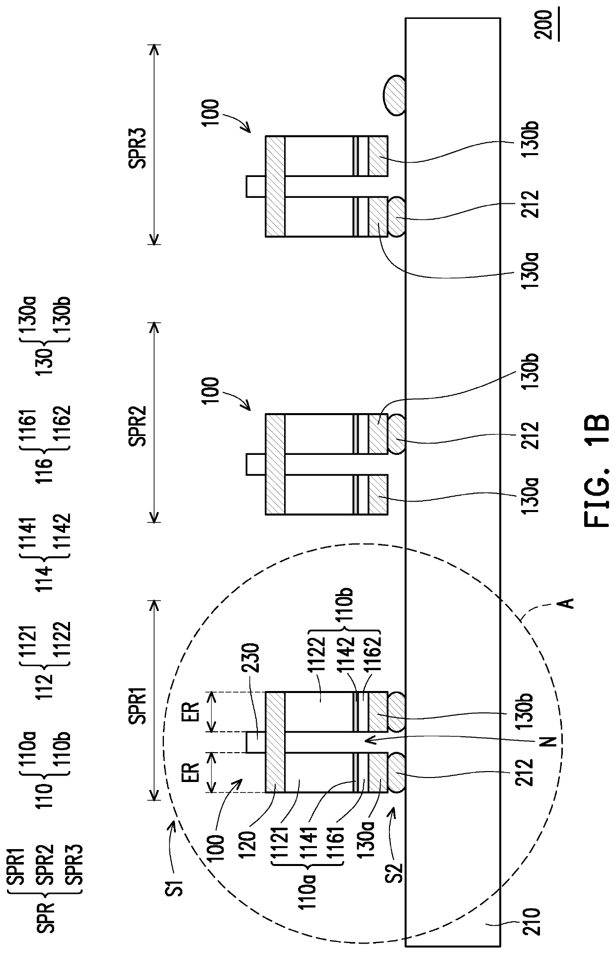
Driving backplane, micro-led display panel and display devices
PatentActiveUS20200111941A1
Innovation
- A driving backplane design with multiple pairs of electrodes, including a main pair and backup pairs, allows for easy replacement of defective LED chips by soldering a normal chip onto backup electrodes, improving the yield of micro-LED display panels and devices.


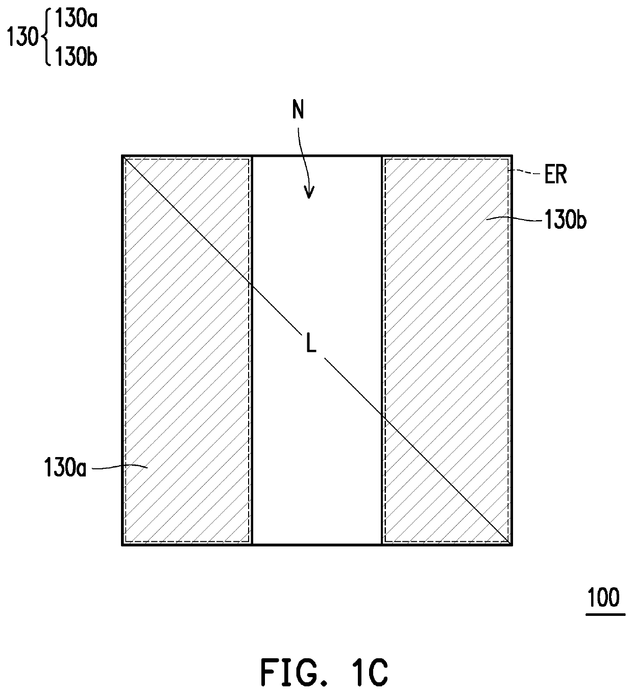
Micro light emitting diode display panel
PatentActiveUS20210280741A1
Innovation
- A micro light emitting diode chip design with multiple second electrodes and light-emitting regions, where successful bonding is enhanced by a larger electrode bonding area, allowing independent control of light-emitting layers and reducing defect pixels, thus improving production yield and image quality without the need for redundant bonding points.

Manufacturing Standards and Quality Control Requirements
The manufacturing standards for MicroLED displays must address the fundamental differences between backplane and monolithic architectures to achieve optimal defect density control. Current industry standards require defect densities below 10^-4 defects per pixel for commercial viability, with premium applications demanding even stricter tolerances. These standards necessitate comprehensive quality control frameworks that account for the distinct failure modes inherent to each manufacturing approach.
For backplane-based MicroLED systems, manufacturing standards emphasize the critical importance of die-to-substrate bonding integrity. Mass transfer processes require precise alignment tolerances within ±1 μm, with bonding strength specifications exceeding 50 MPa to prevent delamination during thermal cycling. Quality control protocols must validate electrical connectivity across millions of individual LED chips, implementing automated optical inspection systems capable of detecting sub-micron defects in real-time during the transfer process.
Monolithic MicroLED manufacturing standards focus primarily on epitaxial growth uniformity and mesa isolation quality. Wafer-level specifications require thickness variations below 2% across 150mm substrates, with stringent controls on threading dislocation densities below 10^6 cm^-2. The standards mandate comprehensive characterization of quantum well structures through photoluminescence mapping, ensuring wavelength uniformity within ±5nm across the entire wafer surface.
Quality control requirements for both architectures incorporate statistical process control methodologies with real-time feedback mechanisms. Inline metrology systems must monitor critical parameters including surface roughness, contamination levels, and electrical characteristics at multiple process stages. Defect classification protocols distinguish between repairable defects, such as particle contamination, and fatal defects like structural damage or electrical opens.
Environmental control standards specify cleanroom classifications of ISO Class 1 or better for critical processing steps, with particular attention to particle control during transfer operations in backplane systems. Temperature and humidity specifications require stability within ±0.1°C and ±1% RH respectively, as thermal fluctuations directly impact yield rates in both manufacturing approaches.
Traceability requirements mandate comprehensive data logging throughout the manufacturing process, enabling rapid identification of defect sources and implementation of corrective actions. These standards establish the foundation for achieving the sub-ppm defect rates necessary for large-area MicroLED display commercialization.
Cost-Performance Trade-offs in MicroLED Architecture Selection
The fundamental cost-performance equation in MicroLED architecture selection hinges on the trade-off between manufacturing complexity and yield optimization. Backplane-based architectures typically require higher initial capital investment due to sophisticated transfer processes and substrate preparation, yet offer superior defect management capabilities through selective die placement and replacement mechanisms.
Manufacturing cost structures differ significantly between approaches. Monolithic integration eliminates transfer-related expenses and reduces substrate material costs, making it attractive for cost-sensitive applications. However, the yield penalty from defective pixels across entire wafers can result in substantial economic losses, particularly as display sizes increase. The cost per functional pixel often favors monolithic approaches only when defect densities remain below critical thresholds.
Performance considerations reveal contrasting optimization paths. Backplane architectures enable heterogeneous integration, allowing optimization of LED performance independently from driving circuitry. This separation facilitates advanced current control, thermal management, and pixel-level compensation algorithms that enhance overall display quality. Monolithic designs sacrifice some performance flexibility but achieve superior electrical characteristics through direct integration and reduced parasitic effects.
Scalability economics present divergent trajectories. Backplane approaches benefit from economies of scale in transfer equipment and substrate reuse, with costs decreasing as production volumes increase. Monolithic manufacturing scales more predictably but faces fundamental yield limitations that become increasingly problematic at larger display dimensions.
The performance-per-dollar metric ultimately depends on application requirements. High-end applications demanding maximum brightness uniformity and pixel-level control justify the premium costs of backplane architectures. Consumer applications prioritizing cost efficiency may accept performance compromises inherent in monolithic designs, provided defect densities remain within acceptable bounds for the target market segment.
Unlock deeper insights with PatSnap Eureka Quick Research — get a full tech report to explore trends and direct your research. Try now!
Generate Your Research Report Instantly with AI Agent
Supercharge your innovation with PatSnap Eureka AI Agent Platform!