

Mitigating Semiconductor Failure by Analyzing Defect Density
MAR 31, 20269 MIN READ
Generate Your Research Report Instantly with AI Agent
PatSnap Eureka helps you evaluate technical feasibility & market potential.
Semiconductor Defect Analysis Background and Objectives
The semiconductor industry has experienced unprecedented growth over the past five decades, driven by continuous miniaturization and performance enhancement demands. As device geometries shrink to nanometer scales, the impact of manufacturing defects on semiconductor reliability has become increasingly critical. Defect density analysis has emerged as a fundamental discipline for understanding and predicting semiconductor failure mechanisms, directly influencing yield optimization and product reliability.
The evolution of semiconductor manufacturing has consistently pushed the boundaries of precision and control. From early micron-scale processes to today's advanced 3nm and beyond technologies, the tolerance for defects has dramatically decreased. What once constituted acceptable defect levels now represents catastrophic failure risks. This paradigm shift has necessitated sophisticated analytical approaches to characterize, quantify, and predict the relationship between defect density and device performance degradation.
Modern semiconductor devices operate under extreme conditions with billions of transistors packed into increasingly compact form factors. The statistical nature of defect distribution means that even low defect densities can significantly impact overall device reliability. Understanding these relationships requires comprehensive analysis methodologies that can correlate physical defect characteristics with electrical performance metrics and long-term reliability projections.
The primary objective of semiconductor defect density analysis is to establish predictive models that enable proactive failure mitigation strategies. This involves developing robust methodologies for defect detection, classification, and correlation with failure modes. Advanced imaging techniques, statistical analysis, and machine learning algorithms are increasingly employed to identify patterns and predict failure probabilities based on defect density distributions.
Contemporary research focuses on multi-scale defect analysis, ranging from atomic-level impurities to wafer-scale variations. The integration of in-line monitoring systems with post-fabrication analysis enables real-time defect density assessment and process optimization. This comprehensive approach aims to minimize defect-induced failures while maintaining manufacturing efficiency and cost-effectiveness.
The ultimate goal extends beyond mere defect detection to encompass predictive maintenance, yield enhancement, and reliability assurance. By establishing clear correlations between defect density metrics and failure mechanisms, manufacturers can implement targeted mitigation strategies, optimize process parameters, and ensure consistent product quality across diverse operating conditions and application environments.
Market Demand for Reliable Semiconductor Manufacturing
The global semiconductor industry faces unprecedented pressure to deliver increasingly reliable products as electronic systems become more complex and mission-critical. Modern applications spanning automotive safety systems, medical devices, aerospace electronics, and data center infrastructure demand semiconductor components with exceptionally low failure rates. This heightened reliability requirement has transformed defect density analysis from a quality control measure into a strategic business imperative.
Market demand for reliable semiconductor manufacturing has intensified significantly due to the proliferation of safety-critical applications. Automotive electronics, particularly in autonomous driving systems, require semiconductor components with failure rates measured in parts per billion rather than traditional parts per million metrics. Similarly, the medical device sector demands ultra-reliable semiconductors for implantable devices and life-support equipment, where component failure could have catastrophic consequences.
The economic implications of semiconductor failures extend far beyond the component cost itself. System-level failures in automotive applications can trigger costly recalls affecting millions of vehicles, while data center outages caused by semiconductor failures can result in substantial revenue losses and reputation damage. This reality has driven end-users to prioritize supplier reliability over cost considerations, creating a premium market for manufacturers who can demonstrate superior defect control capabilities.
Manufacturing yield optimization represents another critical market driver for defect density analysis solutions. As semiconductor geometries continue shrinking and wafer sizes increase, the economic impact of manufacturing defects grows exponentially. Advanced process nodes require sophisticated defect detection and analysis capabilities to maintain acceptable yield levels, making defect density analysis tools essential for competitive manufacturing operations.
The emergence of new application domains such as Internet of Things devices, edge computing, and 5G infrastructure has created diverse reliability requirements across different market segments. Each application category demands tailored approaches to defect analysis and failure mitigation, expanding the total addressable market for specialized semiconductor reliability solutions.
Supply chain resilience concerns have further amplified demand for reliable semiconductor manufacturing capabilities. Recent global supply chain disruptions highlighted the critical importance of semiconductor reliability, prompting governments and corporations to invest heavily in domestic manufacturing capabilities with enhanced quality control systems. This trend has accelerated adoption of advanced defect analysis technologies across both established and emerging semiconductor manufacturing regions.
Current Defect Density Analysis Challenges in Semiconductors
Semiconductor defect density analysis faces significant challenges in achieving the precision and speed required for modern manufacturing environments. Traditional inspection methods often struggle with the increasing complexity of advanced node technologies, where feature sizes continue to shrink while defect detection requirements become more stringent. Current optical inspection systems frequently encounter limitations in resolution and sensitivity, particularly when detecting sub-surface defects or anomalies in three-dimensional structures such as FinFETs and gate-all-around transistors.
The heterogeneous nature of modern semiconductor devices presents another substantial challenge. Different materials, layer compositions, and structural geometries within a single wafer create varying optical and electrical properties that complicate uniform defect detection. Conventional analysis algorithms often fail to adapt to these variations, leading to inconsistent defect classification and false positive rates that can exceed acceptable manufacturing tolerances.
Data processing and analysis speed represent critical bottlenecks in current defect density assessment workflows. High-resolution wafer scanning generates massive datasets that require real-time processing to maintain production throughput. Existing computational frameworks struggle to balance analysis accuracy with processing speed, often forcing manufacturers to choose between comprehensive defect characterization and manufacturing efficiency.
Pattern recognition accuracy remains problematic, particularly for distinguishing between critical defects that impact device functionality and cosmetic anomalies that do not affect performance. Current machine learning models used in defect classification often lack sufficient training data for emerging defect types and struggle with generalization across different process conditions and device architectures.
Integration challenges between multiple inspection tools and analysis platforms create data silos that prevent comprehensive defect correlation analysis. Different inspection systems often use proprietary data formats and coordinate systems, making it difficult to combine results from various measurement points throughout the manufacturing process. This fragmentation limits the ability to establish clear relationships between process parameters and defect formation patterns.
Statistical analysis methodologies currently employed in defect density assessment often rely on sampling approaches that may miss critical low-frequency, high-impact defects. The assumption of random defect distribution does not always hold true for systematic process-related defects, leading to inadequate risk assessment and yield prediction accuracy.
Existing Defect Density Mitigation Solutions
01 Defect detection and measurement methods in semiconductors
Various techniques and apparatus are employed to detect, measure, and analyze defects in semiconductor materials and devices. These methods include optical inspection systems, electron beam techniques, and automated defect classification systems that can identify and quantify different types of defects such as particles, scratches, and crystallographic defects. Advanced imaging and signal processing algorithms enable precise defect density measurements across wafer surfaces.- Defect detection and measurement methods in semiconductors: Various techniques and apparatus have been developed for detecting and measuring defects in semiconductor materials and devices. These methods include optical inspection systems, electron beam inspection, and automated defect classification systems. The techniques enable precise identification of defect types, locations, and densities across semiconductor wafers and chips. Advanced algorithms and image processing methods are employed to distinguish between different defect categories and quantify their impact on device performance.
- Reduction of defect density through manufacturing process optimization: Methods for reducing defect density focus on optimizing semiconductor manufacturing processes including epitaxial growth, deposition, etching, and annealing steps. Process parameters such as temperature, pressure, gas flow rates, and timing are carefully controlled to minimize the formation of crystalline defects, contamination, and structural imperfections. These approaches result in improved material quality and enhanced device yield by addressing defect formation at its source during fabrication.
- Gettering techniques for defect management: Gettering processes are employed to capture and neutralize harmful impurities and defects in semiconductor substrates. These techniques involve creating specific regions or layers that attract and trap contaminants away from active device areas. Various gettering methods include intrinsic gettering through oxygen precipitation, extrinsic gettering using backside damage or polysilicon layers, and phosphorus diffusion gettering. These approaches effectively reduce the impact of defects on device performance without requiring complete elimination of all imperfections.
- Characterization of defect density in specific semiconductor structures: Specialized methods have been developed to characterize defect density in particular semiconductor structures such as epitaxial layers, silicon-on-insulator substrates, compound semiconductors, and thin film materials. These characterization techniques provide quantitative measurements of threading dislocations, stacking faults, point defects, and interface defects. The methods enable correlation between defect density and electrical properties, allowing for quality control and process development in advanced semiconductor manufacturing.
- Impact of defect density on device performance and reliability: Research has established relationships between defect density and semiconductor device characteristics including leakage current, breakdown voltage, carrier mobility, and long-term reliability. Studies demonstrate how different types of defects affect specific device parameters and overall circuit performance. Understanding these relationships enables the establishment of acceptable defect density thresholds for various applications and helps guide manufacturing process improvements. Predictive models have been developed to estimate device yield and reliability based on measured defect densities.
02 Reduction of defect density through manufacturing process control
Manufacturing processes are optimized to minimize defect formation during semiconductor fabrication. This includes controlling deposition parameters, annealing conditions, and cleaning procedures to reduce contamination and structural defects. Process monitoring and feedback systems are implemented to maintain low defect densities throughout production. Specific attention is given to critical steps such as epitaxial growth, ion implantation, and chemical mechanical polishing.Expand Specific Solutions03 Gettering techniques for defect management
Gettering methods are utilized to trap and neutralize harmful impurities and defects in semiconductor substrates. These techniques involve creating intentional defect sites or regions that attract mobile contaminants away from active device areas. Various gettering approaches include backside damage, phosphorus diffusion, and intrinsic gettering through oxygen precipitation. These methods effectively reduce the impact of defects on device performance.Expand Specific Solutions04 Characterization of defect types and their impact on device performance
Different defect types in semiconductors are characterized based on their physical and electrical properties. Point defects, line defects, and planar defects each have distinct effects on carrier mobility, leakage current, and device reliability. Analytical techniques correlate defect density with electrical parameters to establish quality metrics. Understanding the relationship between specific defect types and device degradation enables targeted improvement strategies.Expand Specific Solutions05 Advanced materials and structures for low defect density
Novel semiconductor materials and device structures are developed to inherently minimize defect formation. This includes the use of buffer layers, strain-relaxed substrates, and selective area growth techniques. Advanced materials such as wide bandgap semiconductors and compound semiconductors require specialized approaches to achieve low defect densities. Epitaxial techniques and substrate engineering play crucial roles in producing high-quality crystalline materials with minimal defects.Expand Specific Solutions
Key Players in Semiconductor Defect Analysis Industry
The semiconductor defect density mitigation landscape represents a mature yet rapidly evolving market driven by increasing chip complexity and miniaturization demands. The industry is experiencing significant growth, with the global semiconductor market exceeding $500 billion annually, necessitating advanced defect analysis solutions. Technology maturity varies significantly across market segments, with established foundries like Taiwan Semiconductor Manufacturing Co., Samsung Electronics, and GLOBALFOUNDRIES leading in advanced process nodes, while companies like Applied Materials, Synopsys, and PDF Solutions provide sophisticated defect detection and analysis tools. Memory specialists including SK Hynix, Micron Technology, and Yangtze Memory Technologies are pushing boundaries in 3D architectures, creating new defect challenges. The competitive landscape features both traditional semiconductor giants and emerging players like Rebellions, indicating ongoing innovation in AI-driven defect analysis methodologies and next-generation manufacturing processes.
Samsung Electronics Co., Ltd.
Technical Solution: Samsung implements a multi-layered defect analysis framework that combines optical inspection, e-beam review, and electrical testing to characterize defect density distributions. Their approach utilizes artificial intelligence-driven defect classification systems that can identify subtle pattern variations indicative of process drift or equipment malfunctions. Samsung's methodology incorporates spatial analysis techniques to map defect clustering patterns across wafers and lots, enabling early detection of systematic issues. The company employs advanced yield modeling that correlates defect density metrics with final device performance and reliability parameters. Their system integrates feedback loops between defect analysis results and process control parameters to enable real-time manufacturing adjustments and prevent yield excursions.
Strengths: Vertical integration allows comprehensive control over manufacturing processes and defect mitigation strategies. Weaknesses: Diverse product portfolio may require different defect analysis approaches, increasing system complexity.
Taiwan Semiconductor Manufacturing Co., Ltd.
Technical Solution: TSMC employs advanced statistical process control (SPC) and machine learning algorithms to analyze defect density patterns across wafer fabrication processes. Their approach integrates real-time defect detection systems with predictive analytics to identify potential failure modes before they impact yield. The company utilizes comprehensive defect classification systems that categorize defects by type, location, and severity, enabling targeted process adjustments. TSMC's defect density analysis incorporates both inline inspection data and final test results to establish correlations between manufacturing variations and semiconductor reliability. Their methodology includes advanced pattern recognition techniques to distinguish between systematic and random defects, allowing for more precise root cause analysis and process optimization strategies.
Strengths: Industry-leading manufacturing scale and advanced process technology enable comprehensive data collection. Weaknesses: High complexity of advanced nodes may introduce new defect mechanisms that are difficult to predict.
Core Innovations in Semiconductor Failure Prevention
Defect density calculation method, defect-density calculation program, defect-density calculation apparatus, heat treatment control system and machining control system
PatentActiveUS20220189833A1
Innovation
- A defect density calculation method and system that calculates temporal changes in defect density distribution using an arithmetic function with activation energy, processing temperature, and time as arguments, allowing for accurate prediction of crystal defects in actual pattern sizes.


Method of predicting reliability of semiconductor device, reliability prediction system using the same and storage medium storing program causing computer to execute the same
PatentInactiveUS20090265155A1
Innovation
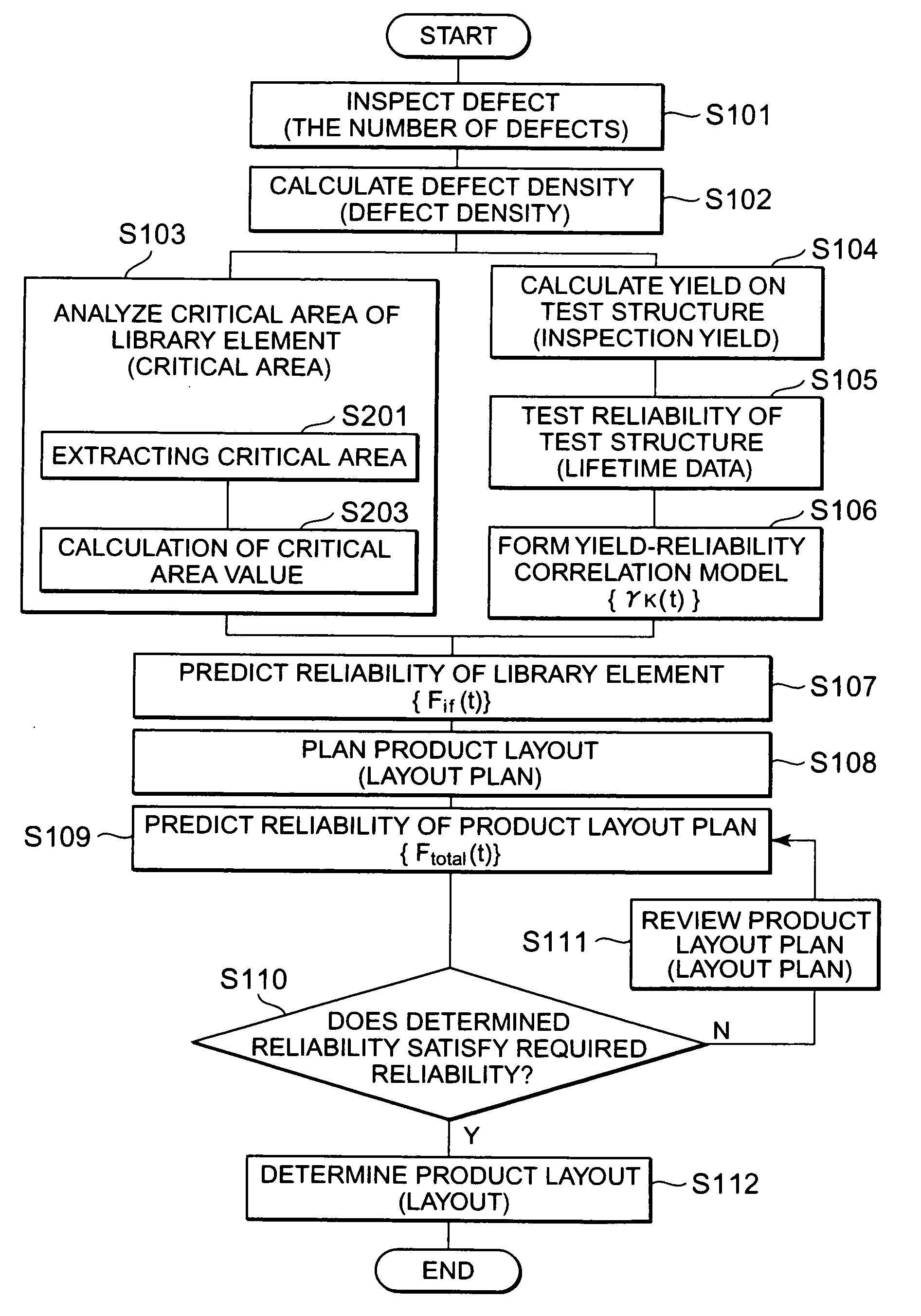
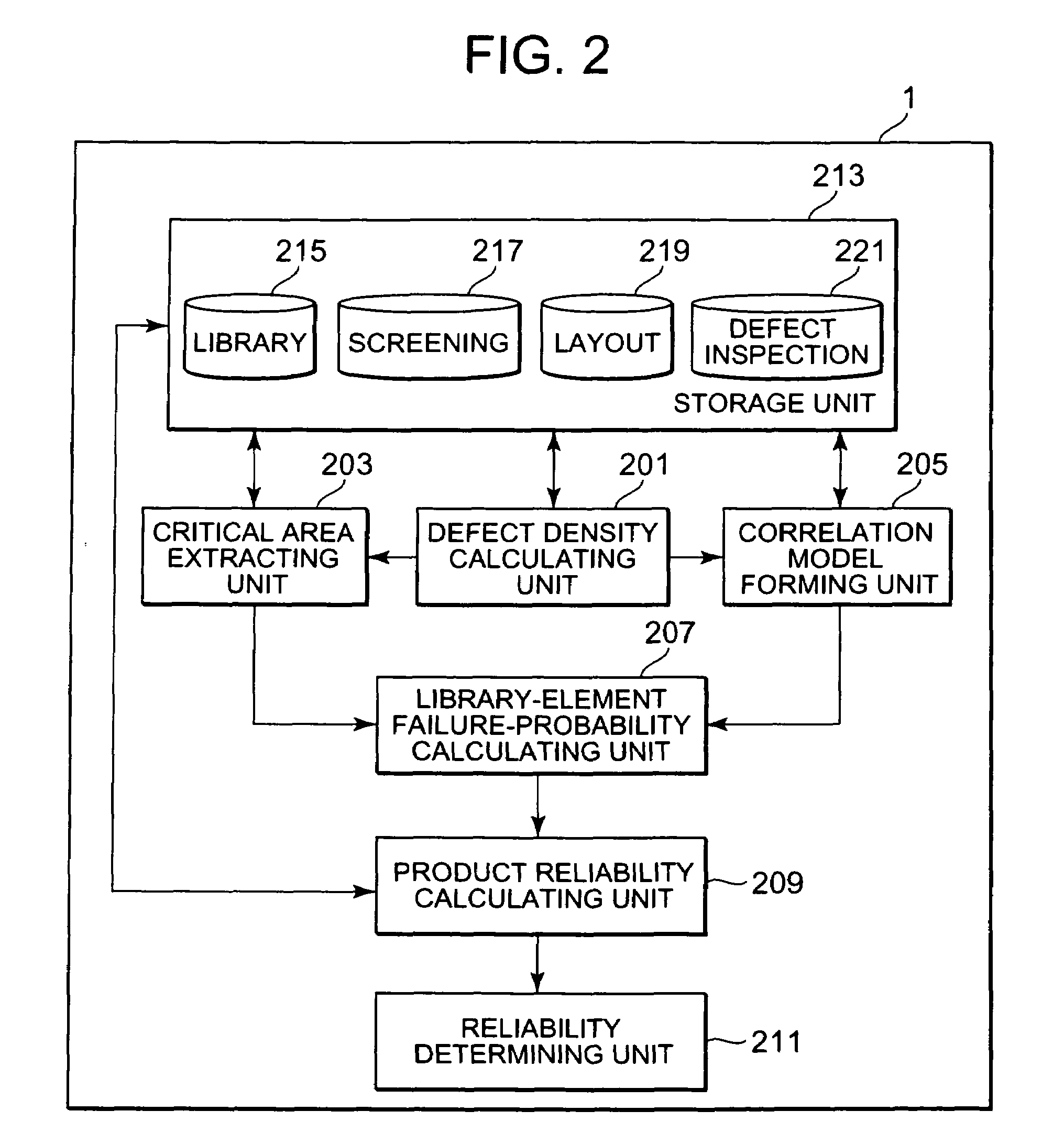
- A method and system that calculate defect density for wiring patterns, extract critical areas for library elements, form a correlation model from failure probabilities and defect occurrence, and use this data to predict the reliability of semiconductor devices before actual design, allowing for initial reliability estimation without post-completion testing.

Quality Standards for Semiconductor Manufacturing
Quality standards in semiconductor manufacturing represent a comprehensive framework designed to ensure consistent product reliability and minimize defect-related failures. These standards encompass multiple dimensions of manufacturing excellence, from raw material specifications to final product validation, establishing measurable criteria that directly correlate with defect density reduction and overall device performance.
The foundation of semiconductor quality standards rests on statistical process control methodologies that define acceptable defect density thresholds across different manufacturing stages. Industry-standard metrics such as Defects Per Million Opportunities (DPMO) and Critical Dimension Uniformity (CDU) provide quantitative benchmarks for evaluating manufacturing performance. These standards typically specify maximum allowable defect densities ranging from 10^-6 to 10^-9 defects per square centimeter, depending on the technology node and application requirements.
International standards organizations, including SEMI, JEDEC, and ISO, have established comprehensive quality frameworks that address defect density management through systematic approaches. SEMI E10 guidelines define equipment reliability standards, while JEDEC standards specify electrical and physical parameters that correlate with defect-free operation. These frameworks mandate rigorous documentation of defect tracking, root cause analysis procedures, and corrective action protocols.
Process-specific quality standards address critical manufacturing steps where defect generation is most likely to occur. Lithography standards define overlay accuracy, critical dimension control, and defect inspection protocols. Chemical mechanical planarization standards specify surface roughness tolerances and particle contamination limits. Each process step incorporates statistical sampling plans and acceptance criteria based on defect density analysis.
Advanced quality standards increasingly incorporate predictive analytics and machine learning algorithms to anticipate potential defect formation before it occurs. These next-generation standards define data collection requirements, algorithm validation procedures, and decision-making protocols that enable proactive defect mitigation strategies, representing a paradigm shift from reactive to predictive quality management approaches.
Cost-Benefit Analysis of Defect Mitigation Strategies
The economic evaluation of defect mitigation strategies in semiconductor manufacturing requires a comprehensive assessment of implementation costs versus potential savings from reduced failure rates. Initial investment considerations include equipment upgrades for advanced inspection systems, process monitoring tools, and data analytics infrastructure. These capital expenditures typically range from hundreds of thousands to millions of dollars depending on facility scale and technology sophistication.
Operational cost analysis encompasses personnel training, increased inspection time, additional consumables, and potential throughput reduction during implementation phases. Advanced defect detection systems may require specialized maintenance contracts and periodic calibration, adding to ongoing operational expenses. However, these costs must be weighed against the substantial savings achieved through early defect identification and prevention.
The benefit side of the equation demonstrates significant value creation through multiple channels. Reduced scrap rates directly translate to material cost savings, while improved yield increases revenue per wafer processed. Early defect detection prevents costly downstream processing of defective units, maximizing resource utilization efficiency. Additionally, enhanced quality control reduces warranty claims and customer returns, protecting brand reputation and maintaining market position.
Quantitative analysis reveals that comprehensive defect mitigation strategies typically achieve return on investment within 12-18 months for high-volume manufacturing facilities. The cost per prevented failure decreases substantially as detection accuracy improves and false positive rates decline. Statistical models indicate that every 1% improvement in defect detection capability can result in 3-5% reduction in overall failure costs.
Long-term financial benefits extend beyond immediate cost savings to include improved customer satisfaction, reduced field failure rates, and enhanced manufacturing predictability. These factors contribute to sustainable competitive advantages and market share growth. Risk mitigation through proactive defect management also reduces exposure to costly product recalls and regulatory compliance issues, providing additional economic value that strengthens the overall business case for strategic defect mitigation investments.
Unlock deeper insights with PatSnap Eureka Quick Research — get a full tech report to explore trends and direct your research. Try now!
Generate Your Research Report Instantly with AI Agent
Supercharge your innovation with PatSnap Eureka AI Agent Platform!