

Optimize Hyperbolic Metamaterials for Transparent Conducting Applications
MAY 14, 202610 MIN READ
Generate Your Research Report Instantly with AI Agent
PatSnap Eureka helps you evaluate technical feasibility & market potential.
Hyperbolic Metamaterial Background and TCE Goals
Hyperbolic metamaterials represent a revolutionary class of artificially engineered structures that exhibit extraordinary optical properties not found in natural materials. These metamaterials are characterized by their hyperbolic dispersion relation, where the permittivity tensor components have opposite signs along different spatial directions. This unique property enables unprecedented control over electromagnetic wave propagation, including enhanced light-matter interactions, negative refraction, and subwavelength imaging capabilities.
The fundamental principle underlying hyperbolic metamaterials lies in their anisotropic structure, typically achieved through alternating layers of metallic and dielectric materials or arrays of metallic nanowires embedded in dielectric hosts. The resulting effective medium exhibits type I or type II hyperbolic dispersion, depending on which permittivity component is negative. This engineered anisotropy creates an infinite density of photonic states, enabling enhanced spontaneous emission, improved light extraction, and novel waveguiding properties.
Historical development of hyperbolic metamaterials began in the early 2000s with theoretical predictions by Podolskiy and Narimanov, followed by experimental demonstrations using metal-dielectric multilayers and nanowire arrays. The field has rapidly evolved from proof-of-concept demonstrations to practical applications in sensing, imaging, and photonic devices. Key milestones include the first experimental verification of hyperbolic dispersion in 2007 and subsequent demonstrations of enhanced emission and super-resolution imaging.
Transparent conducting electrodes represent a critical component in modern optoelectronic devices, including solar cells, displays, touch screens, and light-emitting diodes. Traditional materials like indium tin oxide face limitations including material scarcity, brittleness, and performance degradation at high frequencies. The integration of hyperbolic metamaterials into transparent conducting applications aims to overcome these limitations while providing enhanced functionality.
The primary technical objectives for optimizing hyperbolic metamaterials in transparent conducting applications encompass several key performance metrics. First, achieving high optical transparency across the visible spectrum while maintaining excellent electrical conductivity represents the fundamental challenge. Second, developing scalable fabrication methods that enable large-area processing with consistent material properties is essential for commercial viability.
Additional goals include enhancing mechanical flexibility to enable applications in flexible electronics, improving thermal stability for high-temperature operations, and reducing material costs through alternative material systems. The optimization process must also address wavelength-dependent performance, ensuring broadband transparency while minimizing optical losses. Furthermore, achieving precise control over the hyperbolic frequency range allows tailoring of the metamaterial properties for specific applications, whether in photovoltaics, displays, or emerging quantum technologies.
The fundamental principle underlying hyperbolic metamaterials lies in their anisotropic structure, typically achieved through alternating layers of metallic and dielectric materials or arrays of metallic nanowires embedded in dielectric hosts. The resulting effective medium exhibits type I or type II hyperbolic dispersion, depending on which permittivity component is negative. This engineered anisotropy creates an infinite density of photonic states, enabling enhanced spontaneous emission, improved light extraction, and novel waveguiding properties.
Historical development of hyperbolic metamaterials began in the early 2000s with theoretical predictions by Podolskiy and Narimanov, followed by experimental demonstrations using metal-dielectric multilayers and nanowire arrays. The field has rapidly evolved from proof-of-concept demonstrations to practical applications in sensing, imaging, and photonic devices. Key milestones include the first experimental verification of hyperbolic dispersion in 2007 and subsequent demonstrations of enhanced emission and super-resolution imaging.
Transparent conducting electrodes represent a critical component in modern optoelectronic devices, including solar cells, displays, touch screens, and light-emitting diodes. Traditional materials like indium tin oxide face limitations including material scarcity, brittleness, and performance degradation at high frequencies. The integration of hyperbolic metamaterials into transparent conducting applications aims to overcome these limitations while providing enhanced functionality.
The primary technical objectives for optimizing hyperbolic metamaterials in transparent conducting applications encompass several key performance metrics. First, achieving high optical transparency across the visible spectrum while maintaining excellent electrical conductivity represents the fundamental challenge. Second, developing scalable fabrication methods that enable large-area processing with consistent material properties is essential for commercial viability.
Additional goals include enhancing mechanical flexibility to enable applications in flexible electronics, improving thermal stability for high-temperature operations, and reducing material costs through alternative material systems. The optimization process must also address wavelength-dependent performance, ensuring broadband transparency while minimizing optical losses. Furthermore, achieving precise control over the hyperbolic frequency range allows tailoring of the metamaterial properties for specific applications, whether in photovoltaics, displays, or emerging quantum technologies.
Market Demand for Advanced Transparent Conductors
The global transparent conductor market is experiencing unprecedented growth driven by the proliferation of touchscreen devices, flexible electronics, and next-generation display technologies. Traditional indium tin oxide (ITO) dominates current applications but faces critical limitations including brittleness, high processing temperatures, and supply chain vulnerabilities due to indium scarcity. These constraints create substantial market opportunities for alternative transparent conducting materials that can deliver superior performance characteristics.
Consumer electronics represents the largest demand segment, with smartphones, tablets, and wearable devices requiring increasingly sophisticated transparent conductors. The automotive industry emerges as a rapidly expanding market, driven by smart windshields, heads-up displays, and electric vehicle charging interfaces. Solar photovoltaic applications demand transparent conductors with enhanced optical transmission and reduced sheet resistance to improve energy conversion efficiency.
The flexible electronics revolution creates entirely new market categories requiring transparent conductors that maintain electrical performance under mechanical stress. Foldable displays, electronic textiles, and biomedical sensors represent high-value applications where conventional materials fail to meet performance requirements. These emerging applications demand materials with exceptional mechanical flexibility while preserving optical transparency and electrical conductivity.
Hyperbolic metamaterials present unique advantages for addressing these market demands through their engineered anisotropic properties. Their ability to support high-k propagating modes enables enhanced charge transport while maintaining optical transparency across broad spectral ranges. The tunability of metamaterial properties through structural design offers customization opportunities for specific application requirements that cannot be achieved with conventional materials.
Market drivers include increasing demand for larger display formats, higher resolution requirements, and improved touch sensitivity in consumer devices. The Internet of Things expansion creates demand for transparent conductors in smart windows, transparent antennas, and invisible sensors integrated into architectural elements. Energy harvesting applications require transparent conductors with minimal optical losses and enhanced electrical performance.
Manufacturing scalability represents a critical market consideration, as successful transparent conductor technologies must demonstrate cost-effective production at industrial scales. The market increasingly values materials that can be processed at lower temperatures, reducing manufacturing costs and enabling integration with temperature-sensitive substrates. Environmental sustainability concerns drive demand for materials with reduced environmental impact compared to rare-earth-dependent alternatives.
Regional market dynamics show strong growth in Asia-Pacific driven by electronics manufacturing concentration, while North American and European markets emphasize high-performance applications in automotive and renewable energy sectors. The convergence of these market forces creates substantial opportunities for optimized hyperbolic metamaterials that can address multiple application requirements through engineered material properties.
Consumer electronics represents the largest demand segment, with smartphones, tablets, and wearable devices requiring increasingly sophisticated transparent conductors. The automotive industry emerges as a rapidly expanding market, driven by smart windshields, heads-up displays, and electric vehicle charging interfaces. Solar photovoltaic applications demand transparent conductors with enhanced optical transmission and reduced sheet resistance to improve energy conversion efficiency.
The flexible electronics revolution creates entirely new market categories requiring transparent conductors that maintain electrical performance under mechanical stress. Foldable displays, electronic textiles, and biomedical sensors represent high-value applications where conventional materials fail to meet performance requirements. These emerging applications demand materials with exceptional mechanical flexibility while preserving optical transparency and electrical conductivity.
Hyperbolic metamaterials present unique advantages for addressing these market demands through their engineered anisotropic properties. Their ability to support high-k propagating modes enables enhanced charge transport while maintaining optical transparency across broad spectral ranges. The tunability of metamaterial properties through structural design offers customization opportunities for specific application requirements that cannot be achieved with conventional materials.
Market drivers include increasing demand for larger display formats, higher resolution requirements, and improved touch sensitivity in consumer devices. The Internet of Things expansion creates demand for transparent conductors in smart windows, transparent antennas, and invisible sensors integrated into architectural elements. Energy harvesting applications require transparent conductors with minimal optical losses and enhanced electrical performance.
Manufacturing scalability represents a critical market consideration, as successful transparent conductor technologies must demonstrate cost-effective production at industrial scales. The market increasingly values materials that can be processed at lower temperatures, reducing manufacturing costs and enabling integration with temperature-sensitive substrates. Environmental sustainability concerns drive demand for materials with reduced environmental impact compared to rare-earth-dependent alternatives.
Regional market dynamics show strong growth in Asia-Pacific driven by electronics manufacturing concentration, while North American and European markets emphasize high-performance applications in automotive and renewable energy sectors. The convergence of these market forces creates substantial opportunities for optimized hyperbolic metamaterials that can address multiple application requirements through engineered material properties.
Current State of Hyperbolic Metamaterial TCE Technology
Hyperbolic metamaterial transparent conducting electrodes (HM-TCEs) represent an emerging class of optical materials that leverage engineered anisotropic properties to achieve superior performance compared to conventional transparent conductors. These structures exhibit hyperbolic dispersion characteristics, where the permittivity tensor components have opposite signs, enabling unique optical and electrical functionalities that traditional materials cannot provide.
Current HM-TCE implementations primarily utilize multilayer metal-dielectric architectures, with alternating thin films of metals such as silver, gold, or aluminum paired with dielectric materials like titanium dioxide, aluminum oxide, or silicon dioxide. The typical layer thicknesses range from 5-50 nanometers, carefully engineered to achieve the desired hyperbolic dispersion while maintaining optical transparency in the visible spectrum.
The most advanced HM-TCE designs demonstrate sheet resistances ranging from 10-100 ohms per square, with optical transmittance values exceeding 85% in the visible range. These performance metrics position hyperbolic metamaterials as competitive alternatives to indium tin oxide (ITO), particularly for applications requiring enhanced angular stability and broadband transparency.
Manufacturing techniques for HM-TCEs have evolved to include magnetron sputtering, atomic layer deposition, and electron beam evaporation. These fabrication methods enable precise control over layer thickness uniformity and interface quality, critical factors determining the overall device performance. Recent developments in roll-to-roll processing show promise for large-scale production capabilities.
Key technical challenges currently limiting widespread adoption include interface roughness effects, oxidation stability of metallic layers, and mechanical flexibility constraints. The effective medium approximation breaks down at smaller feature sizes, requiring more sophisticated design approaches that account for spatial dispersion and nonlocal effects.
Research institutions and technology companies are actively developing hybrid approaches that combine hyperbolic metamaterials with graphene, carbon nanotubes, or conducting polymers to address current limitations. These composite structures aim to leverage the complementary properties of different material systems while mitigating individual weaknesses.
Performance optimization efforts focus on reducing optical losses through improved material selection and structural design, while simultaneously enhancing electrical conductivity through better interface engineering and reduced scattering mechanisms.
Current HM-TCE implementations primarily utilize multilayer metal-dielectric architectures, with alternating thin films of metals such as silver, gold, or aluminum paired with dielectric materials like titanium dioxide, aluminum oxide, or silicon dioxide. The typical layer thicknesses range from 5-50 nanometers, carefully engineered to achieve the desired hyperbolic dispersion while maintaining optical transparency in the visible spectrum.
The most advanced HM-TCE designs demonstrate sheet resistances ranging from 10-100 ohms per square, with optical transmittance values exceeding 85% in the visible range. These performance metrics position hyperbolic metamaterials as competitive alternatives to indium tin oxide (ITO), particularly for applications requiring enhanced angular stability and broadband transparency.
Manufacturing techniques for HM-TCEs have evolved to include magnetron sputtering, atomic layer deposition, and electron beam evaporation. These fabrication methods enable precise control over layer thickness uniformity and interface quality, critical factors determining the overall device performance. Recent developments in roll-to-roll processing show promise for large-scale production capabilities.
Key technical challenges currently limiting widespread adoption include interface roughness effects, oxidation stability of metallic layers, and mechanical flexibility constraints. The effective medium approximation breaks down at smaller feature sizes, requiring more sophisticated design approaches that account for spatial dispersion and nonlocal effects.
Research institutions and technology companies are actively developing hybrid approaches that combine hyperbolic metamaterials with graphene, carbon nanotubes, or conducting polymers to address current limitations. These composite structures aim to leverage the complementary properties of different material systems while mitigating individual weaknesses.
Performance optimization efforts focus on reducing optical losses through improved material selection and structural design, while simultaneously enhancing electrical conductivity through better interface engineering and reduced scattering mechanisms.
Existing Hyperbolic Metamaterial TCE Solutions
01 Hyperbolic metamaterial structures for enhanced transparency
Hyperbolic metamaterials can be engineered with specific geometric configurations and material compositions to achieve enhanced optical transparency across different wavelengths. These structures utilize anisotropic properties and carefully designed unit cells to manipulate electromagnetic wave propagation, enabling selective transparency while maintaining desired optical characteristics. The metamaterial design allows for precise control over refractive indices and dispersion properties.- Hyperbolic metamaterial structures for enhanced transparency: Hyperbolic metamaterials can be engineered with specific geometric configurations and material compositions to achieve enhanced optical transparency across different wavelengths. These structures utilize anisotropic properties and carefully designed unit cells to manipulate electromagnetic wave propagation, enabling selective transparency while maintaining desired optical characteristics. The metamaterial design allows for precise control over refractive indices and dispersion properties.
- Conductive metamaterial architectures with hyperbolic dispersion: Advanced metamaterial designs incorporate conductive elements arranged in hyperbolic configurations to achieve unique electrical properties. These architectures combine metallic and dielectric components in periodic or quasi-periodic arrangements that exhibit hyperbolic dispersion characteristics while maintaining electrical conductivity. The structures enable simultaneous control of electromagnetic and electrical transport properties through engineered interfaces and coupling mechanisms.
- Multilayer hyperbolic metamaterial fabrication techniques: Manufacturing methods for creating multilayer hyperbolic metamaterials involve precise deposition and patterning techniques to achieve the required structural periodicity and material distribution. These fabrication approaches include advanced lithography, thin-film deposition, and etching processes that enable the creation of complex three-dimensional metamaterial structures with controlled layer thicknesses and interface properties for optimal performance.
- Tunable optical properties in hyperbolic metamaterials: Dynamic control of optical properties in hyperbolic metamaterials can be achieved through various tuning mechanisms including electrical, thermal, and mechanical approaches. These systems allow real-time adjustment of transparency, reflectance, and transmission characteristics by modifying the metamaterial's effective permittivity and permeability tensors. The tunability enables adaptive optical devices with switchable functionality.
- Applications in electromagnetic wave manipulation: Hyperbolic metamaterials find applications in advanced electromagnetic wave manipulation systems including cloaking devices, super-resolution imaging, and enhanced light-matter interactions. These applications leverage the unique dispersion properties and anisotropic characteristics of hyperbolic metamaterials to achieve functionalities not possible with conventional materials. The technology enables novel approaches to electromagnetic field control and wave engineering.
02 Conductive metamaterial architectures with hyperbolic dispersion
Advanced metamaterial designs incorporate conductive elements arranged in hyperbolic configurations to achieve unique electrical and electromagnetic properties. These architectures utilize metallic components, conductive polymers, or hybrid materials to create anisotropic conductivity patterns while maintaining hyperbolic dispersion characteristics. The conductive pathways are optimized to support specific electromagnetic modes and frequency responses.Expand Specific Solutions03 Multilayer hyperbolic metamaterial fabrication techniques
Manufacturing approaches for hyperbolic metamaterials involve sophisticated multilayer deposition and patterning techniques to create the required anisotropic structures. These methods include advanced lithography, thin-film deposition, and precision etching processes to achieve the necessary geometric precision and material properties. The fabrication techniques enable control over layer thickness, periodicity, and interface quality critical for metamaterial performance.Expand Specific Solutions04 Tunable optical properties in hyperbolic metamaterials
Dynamic control mechanisms enable real-time adjustment of optical and electrical properties in hyperbolic metamaterial systems. These tunable characteristics are achieved through various approaches including voltage control, thermal modulation, and mechanical deformation. The tunability allows for adaptive transparency and conductivity responses, making these materials suitable for active optical devices and smart material applications.Expand Specific Solutions05 Applications in electromagnetic wave manipulation
Hyperbolic metamaterials demonstrate unique capabilities for controlling electromagnetic wave propagation, including wave focusing, beam steering, and frequency selective behavior. These materials exploit their anisotropic properties to achieve unconventional electromagnetic responses not found in natural materials. Applications span across various frequency ranges from optical to microwave, enabling novel device functionalities in telecommunications, sensing, and imaging systems.Expand Specific Solutions
Key Players in Metamaterial and TCE Industry
The hyperbolic metamaterials market for transparent conducting applications is in an early-stage development phase, characterized by significant research activity but limited commercial deployment. The market remains relatively small with most developments concentrated in academic and research institutions rather than large-scale industrial production. Technology maturity varies considerably across the competitive landscape, with leading research organizations like Purdue Research Foundation, Duke University, and Nanyang Technological University driving fundamental breakthroughs in metamaterial design and fabrication. Industrial players including Sumitomo Chemical, Nitto Denko, and TDK Corp are exploring practical applications, while specialized companies like Cambrios Technologies focus on silver nanowire solutions for transparent conductors. The field shows promise for display technologies and optoelectronics, but faces challenges in scalable manufacturing and cost-effectiveness compared to conventional transparent conducting materials like ITO.
Purdue Research Foundation
Technical Solution: Purdue Research Foundation has pioneered theoretical and experimental work on hyperbolic metamaterials for transparent conducting applications through their advanced materials research programs. Their approach focuses on creating artificial anisotropic media using alternating layers of metals and dielectrics with subwavelength thickness, achieving hyperbolic dispersion where the permittivity tensor components have opposite signs. The foundation's research teams have developed novel fabrication methods using magnetron sputtering and molecular beam epitaxy to create multilayer structures with precise thickness control at the nanometer scale. Their metamaterial designs incorporate materials like titanium nitride and aluminum-doped zinc oxide, optimizing the balance between conductivity and transparency through careful engineering of the effective medium properties and plasma frequency matching.
Strengths: Strong fundamental research capabilities and academic expertise in metamaterial theory provide deep understanding of underlying physics. Weaknesses: Limited industrial manufacturing experience and longer technology transfer timelines may delay practical implementation.
Sumitomo Chemical Co., Ltd.
Technical Solution: Sumitomo Chemical has developed hyperbolic metamaterial technologies for transparent conducting applications by leveraging their expertise in advanced materials synthesis and processing. Their approach involves creating structured materials with engineered optical and electrical properties through controlled deposition of metallic and dielectric layers at nanoscale dimensions. The company utilizes their proprietary chemical vapor deposition and solution processing techniques to fabricate metamaterial structures that exhibit hyperbolic dispersion characteristics while maintaining high optical transparency. Their technology focuses on incorporating conductive polymers and metal oxide nanostructures in periodic arrangements, achieving sheet resistance values competitive with conventional transparent conductors while offering improved mechanical flexibility and processing advantages. The metamaterial designs are optimized for applications in flexible electronics and large-area transparent electrodes.
Strengths: Strong chemical processing expertise and established manufacturing infrastructure enable scalable production of metamaterial structures. Weaknesses: Limited experience with complex nanofabrication techniques may constrain the sophistication of achievable metamaterial geometries.
Core Innovations in Hyperbolic TCE Optimization
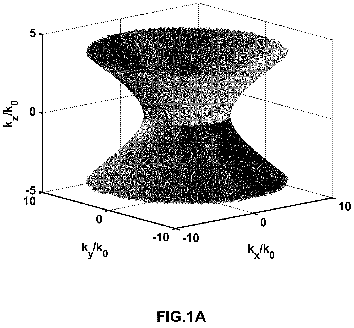
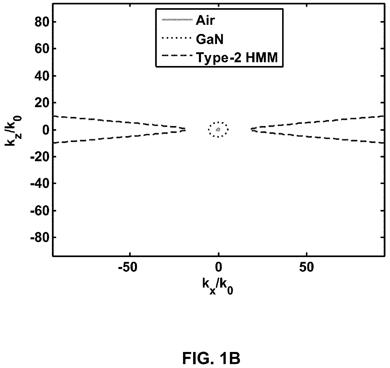
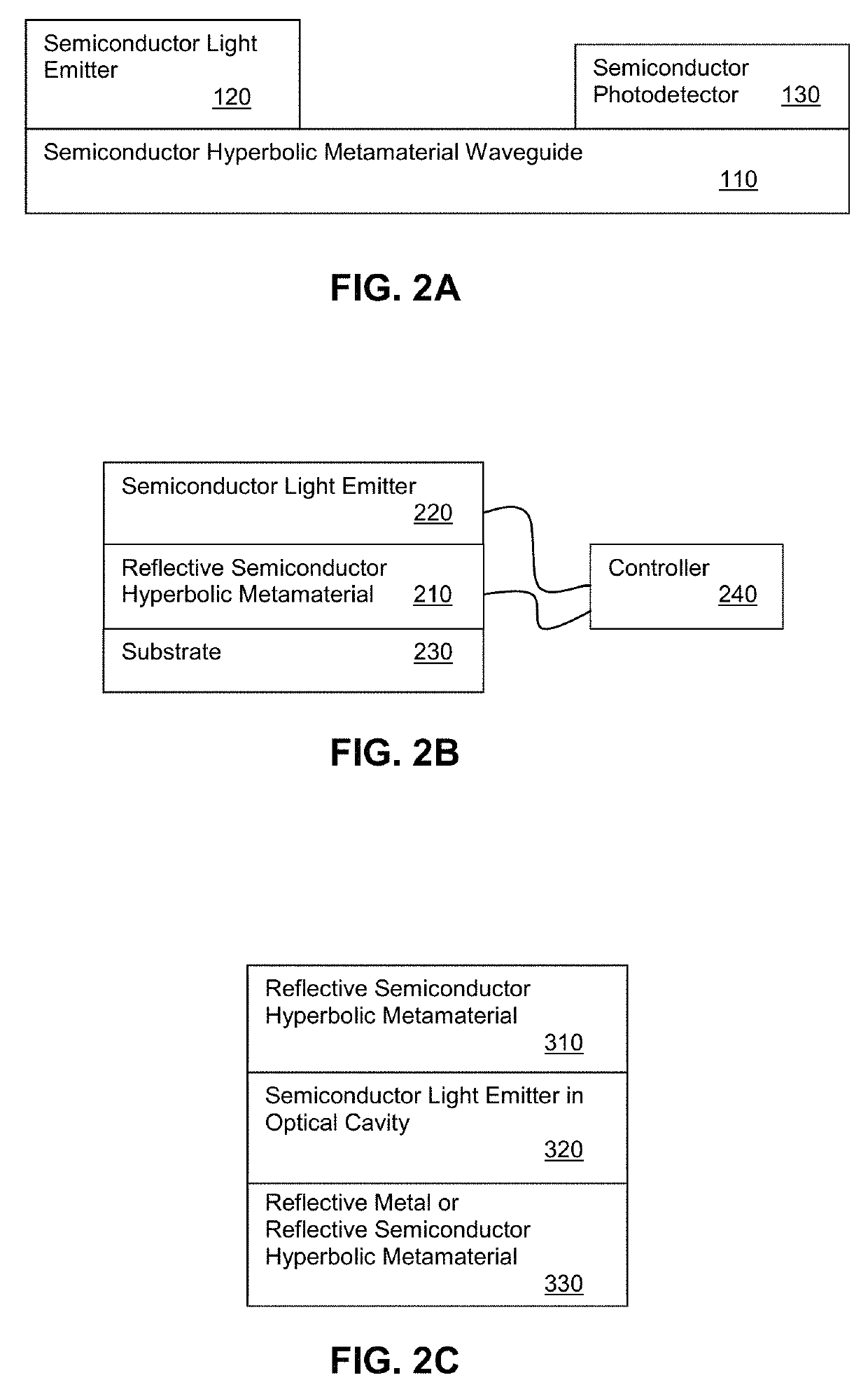
Devices with semiconductor hyperbolic metamaterials
PatentActiveUS11448824B2
Innovation
- Replacing metal layers with a two-dimensional electron or hole gas in semiconductor-based assemblies, where low-doped semiconductor regions act as dielectrics, forming a periodic sequence of electron or hole gas layers to achieve hyperbolic metamaterial properties.

Manufacturing Standards for Metamaterial TCEs
The manufacturing of metamaterial transparent conducting electrodes (TCEs) requires comprehensive standardization frameworks to ensure consistent quality, performance, and scalability across production facilities. Current manufacturing standards are fragmented across different fabrication methodologies, creating significant challenges for industrial adoption and quality assurance in hyperbolic metamaterial applications.
Substrate preparation standards represent a critical foundation for metamaterial TCE manufacturing. Industry protocols must define surface roughness tolerances, typically maintaining Ra values below 0.5 nanometers for optimal metamaterial layer adhesion. Cleaning procedures require standardized chemical treatments and plasma activation parameters to ensure consistent surface energy and contamination-free interfaces. Temperature control during substrate handling must maintain variations within ±2°C to prevent thermal stress-induced defects.
Deposition process standards encompass multiple fabrication techniques including electron beam lithography, nanoimprint lithography, and atomic layer deposition. Each method requires specific parameter control ranges for layer thickness uniformity, typically achieving variations below 5% across substrate areas. Vacuum conditions must maintain base pressures below 10^-8 Torr for high-quality metallic layer formation, while deposition rates require precise control within ±10% of target values to ensure consistent optical and electrical properties.
Pattern fidelity standards address the geometric precision essential for hyperbolic metamaterial functionality. Critical dimension control must maintain feature size variations within ±5 nanometers for sub-wavelength structures. Alignment accuracy between multiple patterning steps requires tolerances below 10 nanometers to preserve the designed electromagnetic response. Edge roughness specifications limit line edge variations to less than 3 nanometers RMS to minimize optical scattering losses.
Quality control protocols establish comprehensive testing methodologies for manufactured metamaterial TCEs. Electrical characterization standards define measurement conditions for sheet resistance uniformity, requiring coefficient of variation below 5% across production batches. Optical transmission measurements must follow standardized spectral ranges and incident angle specifications to ensure comparable performance metrics. Environmental stability testing protocols establish accelerated aging procedures under controlled temperature, humidity, and UV exposure conditions.
Traceability requirements mandate comprehensive documentation throughout the manufacturing process, including material lot tracking, process parameter logging, and performance verification records. Statistical process control implementation requires real-time monitoring of critical parameters with automated feedback systems to maintain production within specification limits.
Substrate preparation standards represent a critical foundation for metamaterial TCE manufacturing. Industry protocols must define surface roughness tolerances, typically maintaining Ra values below 0.5 nanometers for optimal metamaterial layer adhesion. Cleaning procedures require standardized chemical treatments and plasma activation parameters to ensure consistent surface energy and contamination-free interfaces. Temperature control during substrate handling must maintain variations within ±2°C to prevent thermal stress-induced defects.
Deposition process standards encompass multiple fabrication techniques including electron beam lithography, nanoimprint lithography, and atomic layer deposition. Each method requires specific parameter control ranges for layer thickness uniformity, typically achieving variations below 5% across substrate areas. Vacuum conditions must maintain base pressures below 10^-8 Torr for high-quality metallic layer formation, while deposition rates require precise control within ±10% of target values to ensure consistent optical and electrical properties.
Pattern fidelity standards address the geometric precision essential for hyperbolic metamaterial functionality. Critical dimension control must maintain feature size variations within ±5 nanometers for sub-wavelength structures. Alignment accuracy between multiple patterning steps requires tolerances below 10 nanometers to preserve the designed electromagnetic response. Edge roughness specifications limit line edge variations to less than 3 nanometers RMS to minimize optical scattering losses.
Quality control protocols establish comprehensive testing methodologies for manufactured metamaterial TCEs. Electrical characterization standards define measurement conditions for sheet resistance uniformity, requiring coefficient of variation below 5% across production batches. Optical transmission measurements must follow standardized spectral ranges and incident angle specifications to ensure comparable performance metrics. Environmental stability testing protocols establish accelerated aging procedures under controlled temperature, humidity, and UV exposure conditions.
Traceability requirements mandate comprehensive documentation throughout the manufacturing process, including material lot tracking, process parameter logging, and performance verification records. Statistical process control implementation requires real-time monitoring of critical parameters with automated feedback systems to maintain production within specification limits.
Sustainability Impact of Metamaterial TCE Production
The production of metamaterial-based transparent conducting electrodes (TCEs) presents significant environmental considerations that must be evaluated against their potential sustainability benefits. Traditional TCE manufacturing relies heavily on indium tin oxide (ITO), which faces supply chain vulnerabilities due to indium scarcity and energy-intensive extraction processes. Metamaterial TCEs offer a pathway to reduce dependence on rare earth elements through engineered nanostructures that achieve comparable performance using more abundant materials.
Manufacturing processes for hyperbolic metamaterials typically involve advanced lithography techniques, thin-film deposition, and precision etching procedures. These processes require substantial energy inputs and specialized cleanroom environments, contributing to the overall carbon footprint. However, the scalability potential of metamaterial production through roll-to-roll processing and self-assembly methods could significantly reduce per-unit environmental impact compared to current ITO sputtering techniques.
Material selection plays a crucial role in sustainability outcomes. Silver-based metamaterials, while offering excellent optical and electrical properties, raise concerns about resource depletion and mining environmental impacts. Alternative approaches using aluminum, copper, or graphene-based structures present more sustainable material profiles, though they may require optimization to achieve equivalent performance levels.
Life cycle assessment considerations reveal that metamaterial TCEs could offer superior longevity and stability compared to conventional alternatives, potentially extending device lifespans and reducing replacement frequency. This durability advantage becomes particularly significant in large-scale applications such as solar panels and architectural glazing, where extended operational life directly translates to reduced environmental impact per unit of energy generated or building performance delivered.
End-of-life recyclability represents another critical sustainability factor. Metamaterial structures designed with material recovery in mind could enable more efficient separation and reuse of constituent materials compared to current TCE technologies. The development of biodegradable or easily separable metamaterial designs could further enhance the circular economy potential of these advanced materials.
Energy efficiency improvements in final applications must also be considered when evaluating overall sustainability impact. Enhanced optical transmission and reduced electrical resistance in metamaterial TCEs can improve the performance of photovoltaic systems and reduce power consumption in display technologies, creating positive environmental feedback effects that may offset production-related impacts over the device lifetime.
Manufacturing processes for hyperbolic metamaterials typically involve advanced lithography techniques, thin-film deposition, and precision etching procedures. These processes require substantial energy inputs and specialized cleanroom environments, contributing to the overall carbon footprint. However, the scalability potential of metamaterial production through roll-to-roll processing and self-assembly methods could significantly reduce per-unit environmental impact compared to current ITO sputtering techniques.
Material selection plays a crucial role in sustainability outcomes. Silver-based metamaterials, while offering excellent optical and electrical properties, raise concerns about resource depletion and mining environmental impacts. Alternative approaches using aluminum, copper, or graphene-based structures present more sustainable material profiles, though they may require optimization to achieve equivalent performance levels.
Life cycle assessment considerations reveal that metamaterial TCEs could offer superior longevity and stability compared to conventional alternatives, potentially extending device lifespans and reducing replacement frequency. This durability advantage becomes particularly significant in large-scale applications such as solar panels and architectural glazing, where extended operational life directly translates to reduced environmental impact per unit of energy generated or building performance delivered.
End-of-life recyclability represents another critical sustainability factor. Metamaterial structures designed with material recovery in mind could enable more efficient separation and reuse of constituent materials compared to current TCE technologies. The development of biodegradable or easily separable metamaterial designs could further enhance the circular economy potential of these advanced materials.
Energy efficiency improvements in final applications must also be considered when evaluating overall sustainability impact. Enhanced optical transmission and reduced electrical resistance in metamaterial TCEs can improve the performance of photovoltaic systems and reduce power consumption in display technologies, creating positive environmental feedback effects that may offset production-related impacts over the device lifetime.
Unlock deeper insights with PatSnap Eureka Quick Research — get a full tech report to explore trends and direct your research. Try now!
Generate Your Research Report Instantly with AI Agent
Supercharge your innovation with PatSnap Eureka AI Agent Platform!