

Optimizing Photolithography Exposure Systems For Ultimate Pattern Fidelity
FEB 10, 20269 MIN READ
Generate Your Research Report Instantly with AI Agent
PatSnap Eureka helps you evaluate technical feasibility & market potential.
Photolithography Evolution and Pattern Fidelity Goals
Photolithography has undergone remarkable transformation since its inception in the semiconductor industry during the 1960s. Initially developed for printing simple circuit patterns with feature sizes measured in micrometers, the technology has evolved through multiple generations of innovation driven by the relentless pursuit of Moore's Law. Early contact and proximity printing methods gave way to projection lithography systems, which fundamentally changed the industry's capability to achieve finer resolution and better pattern control.
The evolution accelerated dramatically with the introduction of g-line and i-line mercury lamp sources in the 1980s, followed by deep ultraviolet lithography using KrF and ArF excimer lasers in the 1990s and 2000s. Each wavelength reduction enabled smaller feature sizes, but also introduced new challenges in maintaining pattern fidelity. The transition to immersion lithography, where liquid media replaced air between the lens and wafer, represented another breakthrough in extending optical lithography capabilities beyond theoretical limits.
The most recent paradigm shift involves extreme ultraviolet lithography operating at 13.5 nanometer wavelength, enabling single-digit nanometer patterning. This advancement required completely reimagining exposure system architecture, including reflective optics, high-power plasma light sources, and ultra-clean vacuum environments. Simultaneously, multiple patterning techniques emerged as critical enablers, allowing conventional systems to achieve resolutions far beyond their native capabilities through sophisticated process integration.
Pattern fidelity has emerged as the paramount objective in modern photolithography optimization. Beyond simply achieving target critical dimensions, contemporary goals encompass minimizing line edge roughness, controlling local and global critical dimension uniformity within angstrom-level tolerances, and ensuring placement accuracy across entire wafer surfaces. These requirements stem from the physical reality that even nanometer-scale variations can significantly impact device performance, yield, and reliability in advanced nodes.
The industry now targets pattern fidelity metrics that seemed impossible just years ago, including edge placement errors below two nanometers and critical dimension uniformity variations under one nanometer across 300-millimeter wafers. Achieving these goals demands holistic optimization of exposure systems, encompassing optical design, illumination control, stage positioning, thermal management, and computational lithography techniques that correct for systematic variations before patterns reach the wafer.
Market Demand for Advanced Lithography Solutions
The semiconductor industry's relentless pursuit of smaller, faster, and more power-efficient chips has positioned advanced photolithography as a mission-critical technology. As device nodes shrink below 7nm and approach 3nm and beyond, the demand for photolithography exposure systems capable of delivering ultimate pattern fidelity has intensified dramatically. This demand is primarily driven by the proliferation of high-performance computing applications, artificial intelligence accelerators, 5G infrastructure, and advanced mobile processors, all of which require unprecedented levels of transistor density and precision.
Major semiconductor manufacturers and foundries are investing heavily in next-generation lithography capabilities to maintain competitive advantage and meet customer requirements for cutting-edge process nodes. The transition from deep ultraviolet lithography to extreme ultraviolet lithography represents a fundamental shift in manufacturing paradigms, necessitating substantial capital expenditure and technological adaptation. Foundries operating at the technology frontier face mounting pressure to achieve higher yields and tighter process control, making optimization of exposure systems a strategic imperative rather than an incremental improvement.
The market landscape reveals a concentrated demand structure, with leading-edge foundries and memory manufacturers constituting the primary customer base for advanced lithography solutions. These organizations require exposure systems that can consistently reproduce nanoscale patterns with minimal edge placement error, reduced line width roughness, and enhanced overlay accuracy. The economic stakes are substantial, as even marginal improvements in pattern fidelity translate directly into yield enhancement and production cost reduction at high-volume manufacturing scales.
Emerging application domains further amplify market demand. Advanced packaging technologies, including chiplet architectures and heterogeneous integration, impose new requirements for lithography precision across diverse substrate materials and topographies. Photonics integration, quantum computing components, and specialized sensors represent nascent but growing market segments that demand customized lithography solutions with exceptional pattern fidelity characteristics.
The competitive dynamics of the semiconductor ecosystem create a self-reinforcing demand cycle. As industry leaders achieve breakthroughs in lithography optimization, competitive pressure compels followers to adopt similar or superior capabilities, thereby expanding the addressable market for advanced exposure system technologies and optimization methodologies.
Current Exposure System Limitations and Challenges
Contemporary photolithography exposure systems face multifaceted constraints that impede the achievement of ultimate pattern fidelity in advanced semiconductor manufacturing. As critical dimensions shrink below 5nm nodes, the fundamental physics of light-matter interaction presents increasingly severe barriers to precise pattern transfer.
Optical resolution limitations constitute the primary challenge. Despite the adoption of extreme ultraviolet lithography at 13.5nm wavelength, diffraction effects and numerical aperture constraints continue to restrict the minimum resolvable feature size. The Rayleigh criterion dictates theoretical resolution limits, while practical implementations encounter additional degradation from lens aberrations, illumination non-uniformities, and stray light interference. These optical imperfections accumulate across the exposure field, creating systematic pattern placement errors and critical dimension variations.
Thermal management emerges as another critical bottleneck. High-power EUV sources generate substantial heat loads on optical components and photomasks, inducing thermal expansion and refractive index fluctuations. These thermal distortions manifest as nanometer-scale overlay errors and focus drift during exposure, directly compromising pattern fidelity. Current cooling systems struggle to maintain thermal stability within the sub-nanometer tolerances required for next-generation devices.
Photomask defectivity and phase errors significantly degrade pattern transfer accuracy. Even sub-10nm mask defects can propagate through the optical system, causing catastrophic pattern failures. Multilayer mask structures used in EUV lithography exhibit inherent phase variations and reflectivity non-uniformities that distort the aerial image. Mask inspection and repair technologies have not kept pace with shrinking defect tolerance budgets.
Resist material limitations further constrain pattern fidelity. Photoresists must simultaneously satisfy conflicting requirements of high sensitivity, excellent resolution, and low line edge roughness. Stochastic effects in photon absorption and chemical amplification introduce random variations in feature dimensions and positions, particularly problematic at EUV wavelengths where photon shot noise becomes statistically significant.
Vibration isolation and environmental control present ongoing challenges. Sub-nanometer mechanical stability requirements demand sophisticated isolation systems, yet external vibrations from facility infrastructure and internal disturbances from stage motion continuously threaten exposure precision. Atmospheric pressure fluctuations and contamination further degrade optical performance through refractive index variations and lens surface degradation.
Mainstream Exposure Optimization Techniques
01 Optical proximity correction and mask optimization techniques
Pattern fidelity in photolithography can be enhanced through optical proximity correction (OPC) methods that compensate for diffraction and process effects. These techniques involve modifying mask patterns to account for optical distortions, using computational algorithms to predict and correct pattern deviations. Advanced mask optimization methods include the use of assist features, serif additions, and bias adjustments to ensure that the printed patterns on wafers match the intended design with high accuracy.- Optical proximity correction and mask optimization techniques: Pattern fidelity in photolithography can be enhanced through optical proximity correction (OPC) methods that compensate for diffraction effects and process variations. These techniques involve modifying mask patterns to account for optical distortions, using computational algorithms to predict and correct pattern deviations before fabrication. Advanced mask optimization approaches include iterative correction methods, model-based adjustments, and the use of assist features to improve the accuracy of transferred patterns on wafers.
- Illumination source optimization and pupil filtering: Improving pattern fidelity involves optimizing the illumination conditions of the exposure system, including the configuration of light sources and pupil plane filtering. Techniques include off-axis illumination, customized pupil shapes, and polarization control to enhance contrast and resolution. These methods reduce interference effects and improve the depth of focus, resulting in more accurate pattern reproduction across varying process conditions.
- Advanced metrology and pattern inspection systems: Maintaining pattern fidelity requires sophisticated metrology and inspection techniques to detect and quantify deviations from intended designs. These systems employ high-resolution imaging, scatterometry, and computational analysis to measure critical dimensions, overlay accuracy, and defect detection. Real-time feedback mechanisms enable process adjustments to maintain consistent pattern quality throughout production runs.
- Resist material properties and processing optimization: Pattern fidelity is significantly influenced by photoresist characteristics and processing parameters. Optimization involves selecting resist materials with appropriate sensitivity, contrast, and resolution capabilities, as well as controlling development, baking, and exposure conditions. Advanced resist formulations and processing techniques minimize line edge roughness, improve sidewall angles, and reduce pattern collapse to achieve higher fidelity reproduction of mask features.
- Multi-patterning and resolution enhancement technologies: Achieving high pattern fidelity at advanced technology nodes requires multi-patterning strategies and resolution enhancement techniques. These approaches include double or multiple exposure methods, spacer-based patterning, and the integration of complementary lithography technologies. Such techniques enable the creation of features smaller than the optical resolution limit while maintaining pattern accuracy and uniformity across the substrate.
02 Illumination source optimization and pupil filtering
Improving pattern fidelity involves optimizing the illumination conditions of the exposure system. This includes adjusting the numerical aperture, wavelength, and coherence settings of the light source. Pupil filtering techniques and customized illumination modes such as off-axis illumination, annular illumination, and dipole illumination can significantly enhance contrast and resolution. These methods help to reduce optical aberrations and improve the transfer of fine pattern details from mask to wafer.Expand Specific Solutions03 Advanced metrology and process control systems
Maintaining pattern fidelity requires sophisticated metrology systems that can accurately measure critical dimensions, overlay accuracy, and pattern placement errors. Real-time monitoring and feedback control systems enable dynamic adjustments during exposure to compensate for process variations. These systems utilize advanced sensors, image processing algorithms, and statistical process control methods to ensure consistent pattern reproduction across multiple wafers and exposure fields.Expand Specific Solutions04 Resist material properties and processing optimization
The chemical and physical properties of photoresist materials play a crucial role in pattern fidelity. Optimizing resist formulations, including sensitivity, contrast, and resolution characteristics, can improve pattern transfer accuracy. Post-exposure baking, development processes, and anti-reflective coating applications are critical steps that affect the final pattern quality. Advanced resist materials with improved line edge roughness and reduced pattern collapse tendencies contribute to enhanced fidelity.Expand Specific Solutions05 Multi-patterning and resolution enhancement techniques
To achieve higher pattern fidelity beyond the diffraction limits of single exposure systems, multi-patterning techniques such as double patterning, triple patterning, and self-aligned multiple patterning are employed. These methods involve multiple lithography and etching steps to create finer features. Additional resolution enhancement techniques include phase-shift masks, immersion lithography, and extreme ultraviolet lithography, all of which contribute to improved pattern accuracy and reduced critical dimension variations.Expand Specific Solutions
Leading Lithography Equipment Manufacturers Analysis
The photolithography exposure systems market represents a mature yet rapidly evolving sector, driven by semiconductor industry demands for advanced node manufacturing. The competitive landscape is dominated by ASML Holding NV, which holds near-monopoly status in extreme ultraviolet (EUV) lithography technology, representing the industry's most advanced capability. Traditional players like Nikon Corporation and Canon maintain positions in deep ultraviolet (DUV) systems, while emerging competitors including Shanghai Microelectronics Equipment Group pursue technological catch-up strategies. The market exhibits high barriers to entry due to substantial R&D investments and complex intellectual property portfolios. Major foundries such as TSMC, Samsung, and Intel drive demand, while pure-play foundries like GLOBALFOUNDRIES and SMIC represent significant customer segments. Technology maturity varies significantly across nodes, with EUV systems enabling sub-7nm production while DUV systems serve mature process requirements, creating a stratified market structure with estimated values exceeding $20 billion annually.
Nikon Corp.
Technical Solution: Nikon has developed advanced deep ultraviolet (DUV) immersion lithography systems optimized for pattern fidelity through multi-patterning techniques and advanced computational lithography solutions. Their NSR-S635E immersion scanner incorporates sophisticated illumination optimization technologies including flexRay illuminator for precise dose control and advanced lens aberration correction systems. Nikon's approach emphasizes overlay accuracy improvements through enhanced alignment systems and real-time focus control mechanisms. The company has invested significantly in source-mask optimization algorithms and model-based OPC solutions that work synergistically with their hardware platforms. Their lithography systems integrate advanced metrology capabilities for in-situ process monitoring and feedback control, enabling tight CD uniformity and minimizing pattern placement errors across the exposure field for critical layers in advanced logic and memory device manufacturing.
Strengths: Strong expertise in DUV immersion lithography, excellent overlay accuracy, and cost-effective solutions for mature nodes. Weaknesses: Limited presence in cutting-edge EUV technology compared to ASML, smaller market share in advanced node lithography, and reduced R&D investment capacity.
ASML Netherlands BV
Technical Solution: ASML has developed advanced extreme ultraviolet (EUV) lithography systems that achieve pattern fidelity through sophisticated computational lithography and source-mask optimization (SMO) techniques. Their latest high-NA EUV systems utilize a numerical aperture of 0.55 to enable sub-3nm node patterning with enhanced resolution and reduced edge placement errors. The company integrates advanced optical proximity correction (OPC), inverse lithography technology (ILT), and machine learning algorithms to optimize mask patterns and compensate for optical aberrations. Their holistic lithography approach combines hardware innovations in illumination control, advanced metrology systems for real-time process monitoring, and sophisticated software algorithms that predict and correct pattern distortions before exposure, ensuring ultimate pattern fidelity for the most demanding semiconductor manufacturing requirements.
Strengths: Industry-leading EUV technology with highest resolution capability, comprehensive ecosystem integration, and continuous innovation in computational lithography. Weaknesses: Extremely high capital costs, complex maintenance requirements, and limited supplier alternatives creating potential supply chain vulnerabilities.
Critical Patents in Pattern Fidelity Enhancement
Image forming state adjusting system, exposure method and exposure apparatus, and program and information storage medium
PatentInactiveUS7405803B2
Innovation
- An image forming state optimizing system that uses a computer-connected adjustment unit to calculate optimal adjustment amounts for the projection optical system based on known adjustment information and image forming quality data, allowing for precise optimization of the projected image under any target exposure conditions by utilizing a Zernike Sensitivity Chart and wavefront aberration variation tables.


Method for determining lithographic focus and exposure
PatentInactiveUS20080192221A1
Innovation
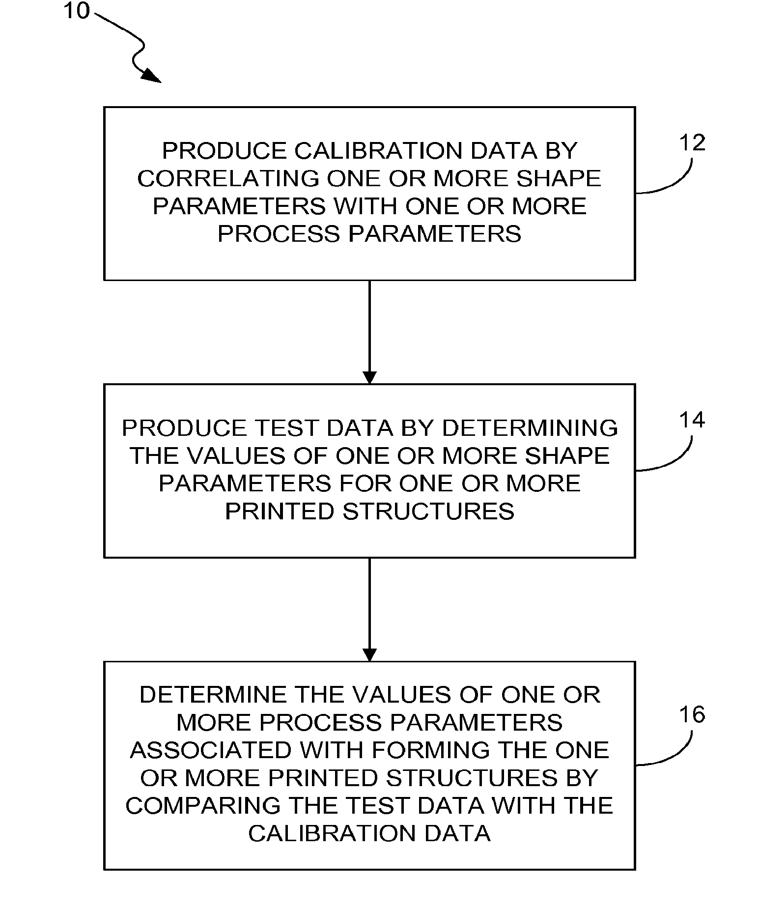
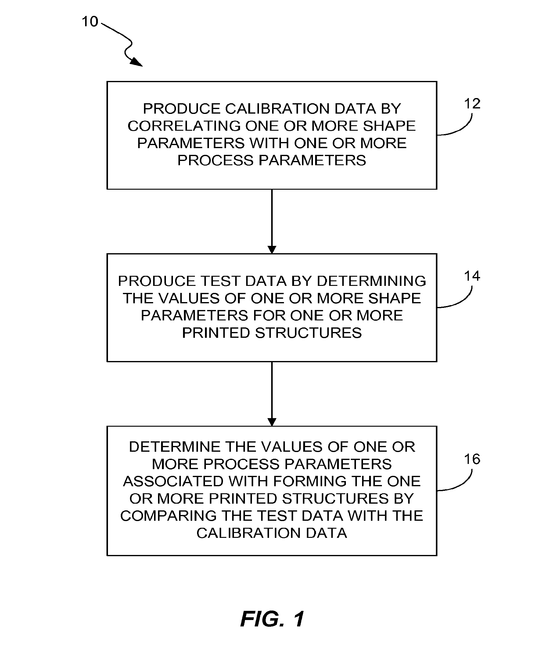
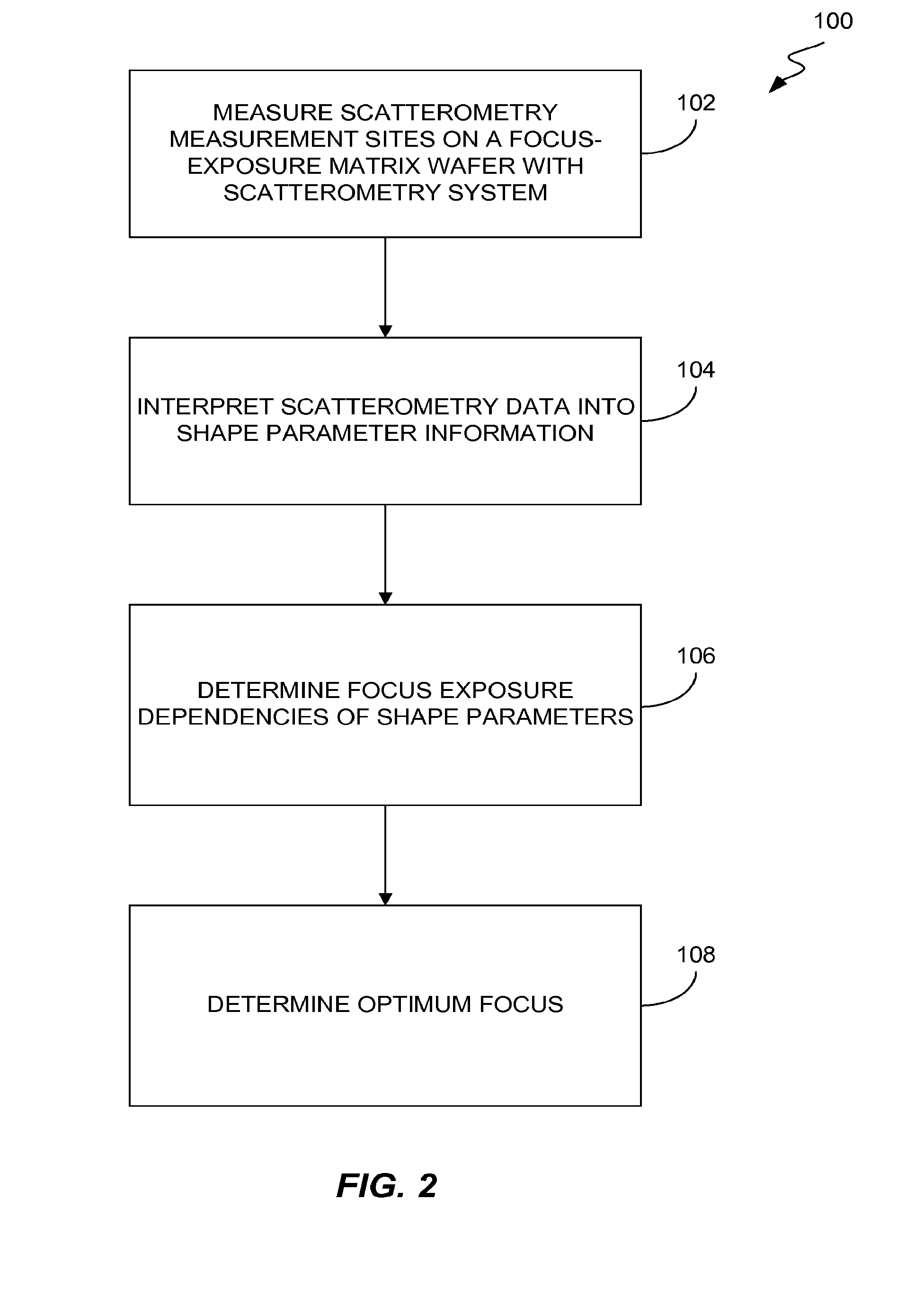
- A method using scatterometry measurements to correlate shape parameters with process parameters, allowing for simultaneous determination of focus and exposure settings on production wafers without stopping production, by interpreting scatterometry data into shape parameter information and matching it with focus exposure dependencies to determine optimal processing conditions.

Semiconductor Manufacturing Standards and Regulations
The semiconductor manufacturing industry operates within a complex framework of standards and regulations that directly impact photolithography exposure system optimization. International standards organizations, particularly SEMI (Semiconductor Equipment and Materials International) and ISO (International Organization for Standardization), establish critical specifications for equipment performance, process control, and quality assurance. These standards define measurement methodologies, calibration procedures, and acceptance criteria that manufacturers must adhere to when developing and deploying advanced lithography systems. Compliance with standards such as SEMI E10 for equipment performance specification and SEMI E35 for guide to calculate cost of ownership metrics ensures consistency across the industry and facilitates technology transfer between fabrication facilities.
Environmental and safety regulations significantly influence the design and operation of photolithography systems. The European Union's REACH (Registration, Evaluation, Authorization and Restriction of Chemicals) regulation and similar frameworks in other jurisdictions impose strict controls on photoresist chemicals, solvents, and cleaning agents used in exposure processes. These regulations drive innovation toward environmentally sustainable materials and closed-loop chemical delivery systems. Additionally, occupational safety standards mandate stringent controls for exposure to deep ultraviolet radiation and hazardous materials, requiring sophisticated containment and monitoring systems integrated into lithography equipment.
Quality management systems governed by standards such as ISO 9001 and automotive-specific IATF 16949 establish rigorous documentation and traceability requirements for pattern fidelity optimization. These frameworks mandate statistical process control methodologies, defect classification systems, and continuous improvement protocols. Semiconductor manufacturers must maintain comprehensive records of exposure parameters, overlay measurements, and critical dimension uniformity data to demonstrate compliance and enable root cause analysis when pattern fidelity issues arise.
Export control regulations, particularly those related to advanced semiconductor manufacturing technology, affect the global distribution and development of cutting-edge photolithography systems. Restrictions imposed by entities such as the Wassenaar Arrangement influence technology collaboration and equipment accessibility, shaping the competitive landscape and regional capabilities in achieving ultimate pattern fidelity. These regulatory constraints necessitate careful consideration of compliance requirements during system design and deployment phases.
Cost-Performance Trade-offs in Lithography Systems
The economics of photolithography systems present fundamental tensions between capital investment, operational costs, and achievable pattern fidelity. Advanced exposure tools represent some of the semiconductor industry's most significant capital expenditures, with extreme ultraviolet lithography systems exceeding $150 million per unit. This substantial upfront investment must be balanced against throughput requirements, yield considerations, and the ultimate quality of pattern transfer. Organizations face critical decisions regarding whether to pursue cutting-edge systems offering superior resolution or optimize existing platforms through incremental improvements and process refinements.
Operational expenditure considerations extend beyond initial equipment acquisition to encompass consumables, maintenance cycles, and facility infrastructure requirements. High numerical aperture immersion systems demand specialized photoresists, topcoat materials, and purified immersion fluids that contribute significantly to per-wafer processing costs. Energy consumption scales dramatically with exposure power requirements, particularly for EUV systems requiring substantial source power to achieve acceptable throughput levels. Clean room specifications, environmental controls, and vibration isolation infrastructure add further operational burden that varies considerably across different lithography architectures.
The relationship between system cost and achievable pattern fidelity exhibits diminishing returns at technology frontiers. While EUV lithography delivers superior single-exposure resolution compared to multi-patterning approaches using ArF immersion tools, the total cost of ownership calculations become complex when factoring throughput limitations, source availability, and mask infrastructure investments. Multi-patterning strategies using mature platforms may achieve comparable effective resolution through multiple exposure steps, trading increased process complexity and cycle time against lower equipment costs and higher tool availability.
Strategic considerations must account for technology roadmap alignment and long-term competitiveness. Early adoption of advanced lithography platforms provides competitive advantages in time-to-market and process capability but carries risks of immature technology and limited supplier ecosystems. Conversely, extended utilization of established systems maximizes return on existing investments while potentially constraining access to leading-edge node capabilities. The optimal balance depends critically on product mix, target markets, and organizational risk tolerance regarding technology transitions.
Unlock deeper insights with PatSnap Eureka Quick Research — get a full tech report to explore trends and direct your research. Try now!
Generate Your Research Report Instantly with AI Agent
Supercharge your innovation with PatSnap Eureka AI Agent Platform!