

Photonics Interposers vs Nanoelectronics: Size Reduction Potential
APR 15, 20269 MIN READ
Generate Your Research Report Instantly with AI Agent
PatSnap Eureka helps you evaluate technical feasibility & market potential.
Photonic Interposer Technology Background and Objectives
Photonic interposer technology represents a paradigm shift in advanced packaging solutions, emerging from the convergence of photonics and electronics integration demands. This technology addresses the fundamental limitations of traditional electronic interconnects by leveraging optical signal transmission within semiconductor packaging architectures. The evolution stems from the increasing bandwidth requirements and power consumption challenges faced by high-performance computing systems, data centers, and telecommunications infrastructure.
The historical development of photonic interposers traces back to early optical communication research in the 1970s, progressing through fiber-optic integration attempts in the 1990s, and culminating in silicon photonics breakthroughs of the 2000s. Key technological milestones include the development of silicon-on-insulator platforms, integrated waveguide structures, and hybrid integration techniques that enable seamless optical-electrical signal conversion within compact form factors.
Current technological objectives focus on achieving unprecedented miniaturization while maintaining signal integrity and bandwidth performance. The primary goal involves developing interposer architectures that can accommodate both photonic and electronic components within sub-millimeter thickness constraints, enabling three-dimensional integration strategies that surpass conventional scaling limitations.
Performance targets encompass achieving data transmission rates exceeding 100 Gbps per channel while reducing power consumption by 80% compared to traditional copper interconnects. Thermal management objectives aim to maintain junction temperatures below 85°C under full operational loads, ensuring reliability in high-density packaging environments.
Manufacturing scalability represents another critical objective, requiring development of fabrication processes compatible with existing semiconductor foundry infrastructure. This includes establishing cost-effective production methodologies that can support volume manufacturing while maintaining the precision required for photonic component integration.
The technology roadmap envisions progressive size reduction capabilities, targeting feature sizes approaching 10-nanometer nodes while incorporating photonic functionalities. Integration density objectives focus on achieving component packing densities exceeding 10^6 elements per square centimeter, enabling system-level miniaturization previously unattainable through purely electronic approaches.
Future technological goals include developing self-aligned assembly processes, advanced materials integration, and novel packaging architectures that can support emerging applications in artificial intelligence, quantum computing, and edge computing platforms where size constraints and performance requirements continue to intensify.
Market Demand for Miniaturized Photonic Integration Solutions
The telecommunications industry represents the largest market segment driving demand for miniaturized photonic integration solutions. Network infrastructure providers are increasingly seeking compact, high-performance optical components to support the exponential growth in data traffic and the deployment of 5G networks. The push toward edge computing and distributed network architectures has intensified requirements for smaller form factors while maintaining or improving optical performance metrics.
Data center operators constitute another critical market segment experiencing unprecedented demand for space-efficient photonic solutions. The continuous expansion of cloud services and artificial intelligence workloads has created urgent needs for higher bandwidth density within constrained physical footprints. Modern hyperscale data centers face significant challenges in power consumption and thermal management, making miniaturized photonic interposers attractive alternatives to traditional electronic interconnects for high-speed data transmission.
Consumer electronics markets are emerging as significant drivers for compact photonic integration, particularly in augmented reality, virtual reality, and advanced display technologies. The integration of photonic components into portable devices requires substantial size reduction while maintaining cost-effectiveness for mass production. This market segment demands solutions that can achieve consumer-grade pricing while delivering professional-level optical performance.
The automotive industry presents growing opportunities for miniaturized photonic solutions, especially in autonomous vehicle systems requiring compact LiDAR sensors and high-speed communication networks. Advanced driver assistance systems increasingly rely on photonic components that must operate reliably in harsh environmental conditions while occupying minimal space within vehicle architectures.
Industrial automation and sensing applications represent expanding market opportunities where size constraints often determine system feasibility. Manufacturing environments require robust photonic solutions that can be integrated into existing equipment without significant modifications to mechanical designs. The trend toward distributed sensing networks in smart manufacturing facilities has created demand for cost-effective, miniaturized photonic components.
Healthcare and biomedical applications are driving specialized demand for ultra-compact photonic integration solutions. Portable diagnostic equipment, implantable devices, and point-of-care testing systems require photonic components with unprecedented miniaturization levels while maintaining precise optical characteristics essential for accurate medical measurements and therapeutic applications.
Current State and Size Limitations of Photonic Interposers
Photonic interposers represent a critical enabling technology for advanced packaging solutions, serving as intermediate substrates that facilitate optical interconnections between electronic components. Currently, these devices integrate optical waveguides, couplers, and passive photonic elements onto silicon or glass substrates, enabling high-bandwidth data transmission while maintaining compatibility with existing electronic packaging infrastructure.
The state-of-the-art photonic interposers typically feature minimum feature sizes ranging from 100 to 500 nanometers for waveguide structures, with coupling elements requiring precise alignment tolerances of less than 1 micrometer. Leading manufacturers have demonstrated interposers with waveguide densities approaching 10-20 channels per millimeter, utilizing silicon-on-insulator (SOI) platforms that leverage mature CMOS fabrication processes.
Current size limitations stem from several fundamental constraints. Optical mode confinement requirements dictate minimum waveguide cross-sections, typically 220-500 nanometers for silicon photonic structures, which are significantly larger than electronic interconnects. Bend radius limitations impose additional spatial constraints, with typical minimum radii of 5-10 micrometers for low-loss operation, restricting routing density compared to electronic traces.
Manufacturing precision presents another critical limitation. Photonic components require sub-nanometer surface roughness control and precise dimensional accuracy to minimize scattering losses. Current lithography capabilities, while advanced, struggle to achieve the uniformity needed for large-scale photonic arrays without significant yield impacts. Edge coupling interfaces demand millimeter-scale keepout zones, further constraining integration density.
Thermal management challenges compound size reduction efforts. Photonic devices exhibit temperature-sensitive performance characteristics, requiring thermal isolation or active temperature control that consumes additional substrate area. The integration of electronic driver circuits alongside photonic elements creates thermal gradients that can degrade optical performance, necessitating careful thermal design considerations.
Despite these constraints, recent advances have pushed photonic interposer integration to new levels. Emerging techniques such as multi-layer photonic routing, vertical coupling architectures, and hybrid integration approaches are beginning to address traditional size limitations while maintaining acceptable performance metrics for next-generation applications.
Existing Miniaturization Solutions for Photonic Systems
01 Silicon photonics interposer integration with electronic circuits
Silicon photonics interposers enable the integration of optical and electronic components on a single substrate, facilitating high-bandwidth data transmission between chips. These interposers utilize silicon-based waveguides and optical interconnects to reduce signal latency and power consumption while maintaining compact form factors. The technology allows for heterogeneous integration of photonic devices with CMOS electronics at reduced dimensions.- Silicon photonics interposer integration with electronic circuits: Silicon photonics interposers enable the integration of optical and electronic components on a single substrate, facilitating high-bandwidth data transmission between chips. These interposers utilize silicon-on-insulator technology to create optical waveguides and coupling structures that connect photonic devices with electronic circuits. The integration approach reduces signal latency and power consumption while enabling compact packaging solutions for high-performance computing applications.
- Nanoelectronic device miniaturization and scaling techniques: Advanced scaling techniques enable the reduction of electronic device dimensions to nanometer scales, improving performance density and reducing power consumption. These techniques include advanced lithography methods, novel transistor architectures, and three-dimensional stacking approaches. The miniaturization strategies address challenges related to quantum effects, heat dissipation, and manufacturing precision at the nanoscale.
- Interposer substrate materials and fabrication methods: Various substrate materials and fabrication techniques are employed to create interposers that bridge different chip technologies. These include glass, organic, and silicon substrates with through-substrate vias for vertical interconnection. The fabrication methods optimize electrical performance, thermal management, and mechanical reliability while accommodating different chip sizes and connection densities.
- Three-dimensional integration and packaging architectures: Three-dimensional integration approaches stack multiple device layers vertically to achieve higher integration density and shorter interconnection paths. These architectures utilize advanced bonding techniques, micro-bump connections, and redistribution layers to create compact multi-chip modules. The packaging solutions address thermal management, signal integrity, and manufacturing yield challenges associated with vertical integration.
- Optical coupling and alignment structures for photonic integration: Precision optical coupling structures enable efficient light transmission between photonic components and optical fibers or waveguides. These structures include grating couplers, edge couplers, and lens systems designed to minimize insertion loss and maximize alignment tolerance. The coupling mechanisms accommodate manufacturing variations while maintaining high optical performance across different wavelengths and polarization states.
02 Nanoelectronic device miniaturization through advanced lithography
Advanced lithography techniques enable the fabrication of nanoelectronic devices with feature sizes below 10 nanometers. These methods include extreme ultraviolet lithography and electron beam lithography, which allow for precise patterning of nanoscale structures. The miniaturization improves device density, reduces power consumption, and enhances performance in integrated circuits.Expand Specific Solutions03 Three-dimensional interposer architectures for vertical integration
Three-dimensional interposer structures enable vertical stacking of multiple device layers, significantly reducing the footprint of electronic systems. Through-silicon vias and microbumps facilitate electrical connections between stacked dies, while maintaining thermal management capabilities. This architecture supports higher integration density and shorter interconnect lengths for improved signal integrity.Expand Specific Solutions04 Quantum dot and nanowire integration in photonic devices
Quantum dots and nanowires serve as active components in photonic interposers, enabling light emission, detection, and modulation at nanoscale dimensions. These nanostructures exhibit quantum confinement effects that enhance optical properties and allow for wavelength-specific operations. Integration of such elements enables compact photonic circuits with improved efficiency and reduced size.Expand Specific Solutions05 Packaging technologies for ultra-compact photonic-electronic modules
Advanced packaging solutions address the challenges of combining photonic and electronic components in minimal space while ensuring thermal dissipation and signal integrity. Techniques include flip-chip bonding, wafer-level packaging, and embedded optical elements that reduce overall module dimensions. These approaches enable system-on-package configurations with reduced parasitic effects and improved performance density.Expand Specific Solutions
Key Players in Photonic Interposer and Nanoelectronics
The photonics interposers versus nanoelectronics competition represents an emerging technology battleground in the early commercialization stage, with market potential reaching billions as demand for miniaturized, high-performance computing solutions intensifies. Technology maturity varies significantly across players, with established semiconductor giants like Samsung Electronics, Advanced Micro Devices, and Infineon Technologies leveraging existing fabrication capabilities, while specialized photonics companies like Lightmatter focus on light-based processing innovations. Research institutions including MIT, Cornell University, and RWTH Aachen University drive fundamental breakthroughs, while companies like SMOLTEK and Bandgap Engineering pioneer nanostructure fabrication techniques. The competitive landscape shows traditional electronics manufacturers adapting photonic integration approaches, while pure-play photonics startups pursue disruptive light-based architectures, creating a dynamic ecosystem where size reduction potential depends on successfully merging photonic and nanoelectronic technologies.
Lightmatter, Inc.
Technical Solution: Lightmatter develops photonic interconnect solutions that leverage silicon photonics technology to create high-bandwidth, low-latency communication systems for AI and datacenter applications. Their photonic interposer technology integrates optical waveguides directly into silicon substrates, enabling massive parallel data transmission with significantly reduced power consumption compared to traditional electrical interconnects. The company's approach focuses on creating compact photonic chips that can handle terabit-scale data rates while maintaining small form factors suitable for modern computing architectures.
Strengths: Leading expertise in commercial photonic interconnects, proven scalability for AI workloads. Weaknesses: Limited to specific high-performance computing applications, higher manufacturing complexity than traditional electronics.
Samsung Electronics Co., Ltd.
Technical Solution: Samsung has developed advanced photonic interposer technologies as part of their semiconductor roadmap, focusing on integrating optical components with their existing CMOS manufacturing processes. Their approach combines traditional nanoelectronics scaling with photonic elements to create hybrid systems that can achieve both electrical miniaturization and optical performance benefits. The company leverages their extensive fab capabilities to manufacture photonic interposers at scale, targeting applications in high-performance computing, 5G infrastructure, and advanced memory systems where both size reduction and bandwidth enhancement are critical.
Strengths: Massive manufacturing scale, integration with existing semiconductor processes, strong R&D resources. Weaknesses: Focus primarily on high-volume applications, less specialized than pure-play photonics companies.
Core Innovations in Photonic-Electronic Integration
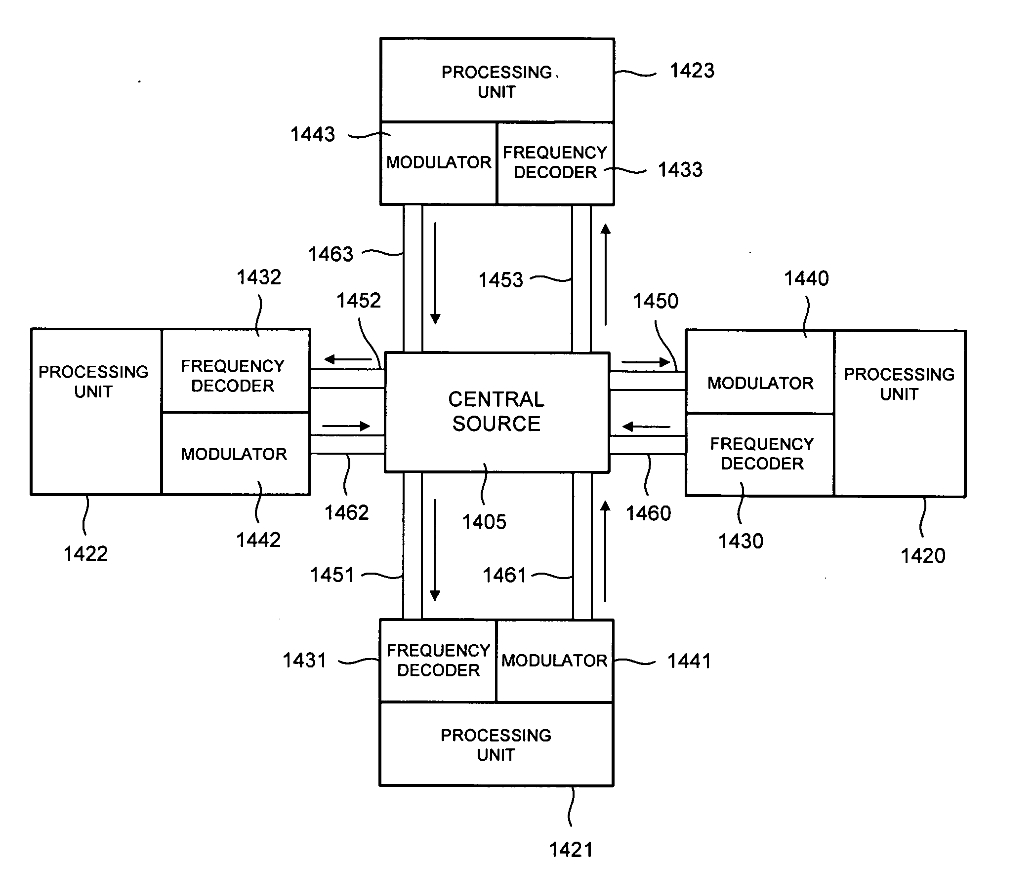
Photonic interconnections that include optical transmission paths for transmitting optical signals
PatentInactiveUS20060056758A1
Innovation
- The implementation of photonic interconnection architectures using optical transmission paths and photonic crystals to transmit multiple independent frequency channels, allowing for high-speed data and clock signal distribution without the size and signal-speed constraints of traditional electrical interconnections.

A photonic interposer, a photonic arrangement and a method for manufacturing a photonic interposer
PatentWO2022253405A1
Innovation
- A photonic interposer with a polarization selective beam splitter/combiner is used to couple light between optical fibers and a photonic integrated circuit, incorporating glass-molded micro-optics with thin film coatings for polarization management, allowing for reduced size and increased scalability by handling mixed polarization light without additional modulators, and enabling efficient coupling of multiple fibers.


Manufacturing Standards for Photonic Integration
The manufacturing standards for photonic integration represent a critical foundation for realizing the size reduction potential when comparing photonics interposers with nanoelectronics solutions. Current standardization efforts focus on establishing consistent fabrication protocols that enable reliable production of compact photonic devices while maintaining performance specifications comparable to traditional electronic counterparts.
Silicon photonics manufacturing has emerged as the dominant platform, leveraging existing CMOS fabrication infrastructure to achieve cost-effective production. The IEEE 802.3 standards committee has developed specifications for photonic transceivers, while organizations like SEMI have established equipment and materials standards for photonic wafer processing. These standards define critical parameters including waveguide dimensions, coupling tolerances, and packaging requirements that directly impact achievable device miniaturization.
Dimensional tolerances represent a fundamental challenge in photonic integration manufacturing. Unlike nanoelectronics where feature sizes continue shrinking through advanced lithography, photonic devices are constrained by wavelength-dependent limitations. Manufacturing standards must accommodate these physical constraints while enabling sufficient integration density to compete with electronic solutions. Current standards specify waveguide width tolerances of ±10 nanometers and coupling alignment accuracies within ±50 nanometers.
Packaging standards play a crucial role in determining overall system size reduction potential. The Optical Internetworking Forum has established multi-source agreements defining form factors for photonic modules, with recent emphasis on co-packaged optics standards that enable closer integration with electronic processing units. These standards address thermal management, electrical interfaces, and mechanical constraints that influence the practical size advantages of photonic interposers.
Quality control and testing standards ensure manufacturing consistency across different foundries and production lines. Standardized measurement protocols for optical loss, crosstalk, and bandwidth characteristics enable reliable comparison between photonic and nanoelectronic solutions. The International Electrotechnical Commission has developed testing standards specifically for integrated photonic devices, establishing benchmarks for performance verification in high-density integration scenarios.
Emerging standards development focuses on heterogeneous integration approaches that combine photonic and electronic components on single substrates. These standards address interface specifications, thermal compatibility, and electrical isolation requirements necessary for achieving maximum size reduction benefits while maintaining system reliability and performance standards expected in commercial applications.
Cost-Performance Trade-offs in Photonic Miniaturization
The economic viability of photonic miniaturization presents a complex landscape where traditional cost-performance paradigms face significant challenges. Unlike electronic components where Moore's Law historically drove simultaneous improvements in performance and cost reduction, photonic devices exhibit fundamentally different scaling behaviors that create unique trade-off scenarios.
Manufacturing costs for miniaturized photonic interposers demonstrate non-linear scaling characteristics. Advanced lithography techniques required for sub-micron photonic structures demand sophisticated fabrication processes, including electron beam lithography and deep UV photolithography, which substantially increase production expenses. The precision requirements for maintaining optical coupling efficiency in reduced form factors necessitate tighter manufacturing tolerances, directly impacting yield rates and driving up per-unit costs.
Performance metrics in miniaturized photonic systems reveal counterintuitive relationships with size reduction. While smaller footprints offer advantages in integration density and reduced parasitic effects, they simultaneously introduce challenges in optical loss management and thermal dissipation. The fundamental physics of light propagation in confined geometries creates inherent limitations where aggressive miniaturization can compromise signal integrity and increase insertion losses.
Economic analysis indicates that the cost-performance sweet spot for photonic interposers occurs at intermediate scaling levels rather than maximum miniaturization. This optimal range typically involves feature sizes between 100-500 nanometers, where manufacturing complexity remains manageable while achieving meaningful performance improvements. Beyond this threshold, exponential cost increases often outweigh marginal performance gains.
Market dynamics further complicate the cost-performance equation. High-volume applications such as data center interconnects can absorb higher per-unit costs due to the substantial performance benefits and energy savings achieved through photonic integration. Conversely, consumer applications require aggressive cost optimization, potentially limiting the viable miniaturization approaches.
The competitive landscape reveals divergent strategies among industry players. Some organizations pursue maximum miniaturization to achieve performance leadership, accepting higher costs as a market differentiation strategy. Others focus on cost-optimized designs that balance moderate miniaturization with manufacturing scalability, targeting broader market adoption through improved economic accessibility.
Unlock deeper insights with PatSnap Eureka Quick Research — get a full tech report to explore trends and direct your research. Try now!
Generate Your Research Report Instantly with AI Agent
Supercharge your innovation with PatSnap Eureka AI Agent Platform!