

Reducing Semiconductor Defect Propagation over Production Cycles
MAR 31, 202610 MIN READ
Generate Your Research Report Instantly with AI Agent
PatSnap Eureka helps you evaluate technical feasibility & market potential.
Semiconductor Defect Control Background and Objectives
The semiconductor industry has experienced unprecedented growth over the past five decades, driven by continuous miniaturization and performance improvements following Moore's Law. However, as device geometries shrink to nanometer scales and manufacturing processes become increasingly complex, defect control has emerged as one of the most critical challenges facing the industry. Traditional defect management approaches that were effective for larger feature sizes are proving inadequate for advanced nodes below 10nm.
Semiconductor defects encompass a broad spectrum of anomalies including particle contamination, pattern defects, material impurities, and process-induced variations. These defects can originate from various sources throughout the manufacturing process, from wafer preparation and lithography to etching, deposition, and packaging. What makes defect propagation particularly problematic is its cumulative nature across production cycles, where minor defects in early stages can amplify into critical failures in subsequent processes.
The evolution of semiconductor manufacturing has introduced new complexities in defect behavior. Multi-patterning lithography, extreme ultraviolet exposure, atomic layer deposition, and three-dimensional device architectures have created novel defect mechanisms that were previously unknown. These advanced processes often involve hundreds of individual steps, each presenting opportunities for defect introduction and propagation.
Current industry data indicates that defect-related yield losses can account for 15-30% of total production costs in advanced semiconductor fabs. The economic impact extends beyond immediate yield losses to include increased cycle times, reduced equipment utilization, and elevated maintenance costs. As production volumes scale and device complexity increases, the compounding effect of defect propagation across multiple production cycles threatens both profitability and supply chain stability.
The primary objective of reducing semiconductor defect propagation is to establish comprehensive control mechanisms that prevent defect amplification throughout the manufacturing lifecycle. This involves developing predictive models that can identify potential defect sources before they impact production, implementing real-time monitoring systems capable of detecting anomalies at the earliest possible stages, and creating adaptive process control strategies that can automatically adjust parameters to minimize defect formation.
A secondary objective focuses on establishing robust defect classification and tracking systems that enable precise correlation between process conditions and defect outcomes. This capability is essential for implementing effective feedback loops that continuously improve process stability and reduce the likelihood of defect recurrence across subsequent production cycles.
Market Demand for High-Yield Semiconductor Manufacturing
The semiconductor industry faces unprecedented pressure to achieve higher manufacturing yields as device complexity continues to escalate and market demands intensify. Modern semiconductor fabrication involves hundreds of intricate process steps, where even minor defects can cascade through production cycles, resulting in substantial yield losses and economic impact. The market demand for high-yield semiconductor manufacturing has become a critical driver for technological advancement and competitive positioning.
Consumer electronics markets, particularly smartphones, tablets, and automotive applications, require increasingly sophisticated chips with higher performance and reliability standards. These applications demand near-zero defect tolerance, as single chip failures can compromise entire system functionality. The automotive sector, especially with the rise of electric vehicles and autonomous driving technologies, has established stringent quality requirements that directly translate to yield expectations exceeding traditional consumer electronics standards.
Data center and cloud computing infrastructure represents another significant demand driver, where high-performance processors and memory devices must maintain exceptional reliability over extended operational periods. The proliferation of artificial intelligence and machine learning applications has created substantial demand for specialized semiconductors with complex architectures, making defect control even more challenging yet essential for market viability.
The economic implications of yield improvement extend beyond individual manufacturers to the entire supply chain. Higher yields directly correlate with reduced production costs, enabling more competitive pricing and broader market accessibility. This economic pressure has intensified as semiconductor manufacturing costs continue rising with each technology node advancement, making yield optimization a fundamental business imperative rather than merely a technical goal.
Emerging applications in Internet of Things devices, 5G infrastructure, and edge computing create additional market segments with distinct yield requirements. These applications often demand cost-effective solutions while maintaining reliability standards, creating a complex balance between manufacturing efficiency and quality control. The market increasingly rewards manufacturers who can consistently deliver high-yield production capabilities across diverse product portfolios.
The competitive landscape has evolved to prioritize yield performance as a key differentiator, with customers increasingly selecting suppliers based on their demonstrated ability to maintain consistent, high-yield manufacturing processes. This market dynamic has transformed defect reduction from a manufacturing concern into a strategic business advantage that directly influences market share and profitability.
Current Defect Propagation Issues in Fab Production
Semiconductor fabrication facilities face significant challenges in controlling defect propagation across production cycles, with contamination being one of the most critical issues. Particle contamination from various sources including process equipment, cleanroom environments, and material handling systems can accumulate on wafer surfaces and transfer between processing steps. These particles often originate from mechanical wear of equipment components, chemical residues from previous processes, or inadequate purification of process gases and chemicals.
Cross-contamination between wafers represents another major propagation pathway, particularly in batch processing equipment where multiple wafers are processed simultaneously. When defective wafers containing high particle counts or chemical residues are processed alongside clean wafers, contamination can transfer through shared process chambers, carrier systems, or handling mechanisms. This issue is especially pronounced in high-temperature processes where volatile contaminants can redistribute across the entire batch.
Equipment-related defect propagation occurs through several mechanisms including chamber seasoning effects, where process byproducts accumulate on chamber walls and subsequently redeposit on wafers in later cycles. Plasma etching and deposition tools are particularly susceptible to this phenomenon, as polymer buildup and metal sputtering can create unstable surface conditions that release particles unpredictably. Additionally, mechanical components such as wafer handling robots and transfer systems can develop wear patterns that generate particles consistently across multiple production lots.
Process drift and tool aging contribute to systematic defect propagation patterns that evolve over extended production periods. As equipment components age, their performance characteristics change subtly, leading to gradual increases in defect generation rates. Temperature uniformity degradation, gas flow instabilities, and electrode erosion in plasma systems create conditions where defects not only increase in frequency but also develop spatial correlation patterns that persist across wafer lots.
Chemical contamination propagation presents unique challenges due to its often invisible nature and delayed manifestation. Trace metal contamination from process chemicals or equipment corrosion can accumulate in process lines and systematically contaminate subsequent wafers. Organic contamination from photoresist stripping processes or solvent cleaning steps can create residual films that interfere with subsequent processing steps, leading to defects that appear cycles after the initial contamination event.
The interconnected nature of modern fab operations amplifies defect propagation risks, as wafers move through multiple process modules and tools within integrated processing systems. Contamination introduced at any point in the process flow can propagate downstream, affecting multiple process steps and potentially impacting entire production lots before detection through routine monitoring systems.
Existing Defect Mitigation Solutions in Production
01 Defect detection and inspection methods in semiconductor manufacturing
Advanced inspection techniques are employed to detect and identify defects in semiconductor wafers during various manufacturing stages. These methods utilize optical inspection systems, electron beam inspection, and image processing algorithms to locate surface and subsurface defects. The detection systems can identify particle contamination, pattern defects, and structural anomalies that may propagate through subsequent processing steps. Automated defect classification and analysis enable early intervention to prevent defect propagation.- Defect detection and inspection methods in semiconductor manufacturing: Advanced inspection techniques are employed to detect and identify defects in semiconductor wafers during various manufacturing stages. These methods utilize optical inspection systems, electron beam inspection, and image processing algorithms to locate surface and subsurface defects. The detection systems can identify particle contamination, pattern defects, and structural anomalies that may propagate through subsequent processing steps. Automated defect classification and analysis enable real-time monitoring and quality control.
- Defect propagation modeling and prediction: Computational models and simulation techniques are developed to predict how defects propagate through multiple layers and processing steps in semiconductor fabrication. These models analyze the relationship between initial defects and their evolution during subsequent manufacturing processes such as etching, deposition, and lithography. Machine learning algorithms and statistical analysis methods are applied to predict defect propagation patterns and assess their impact on device yield and performance.
- Defect mitigation and prevention strategies: Various techniques are implemented to prevent defect formation and minimize their propagation during semiconductor processing. These strategies include optimized process parameters, improved cleaning procedures, and enhanced material quality control. Barrier layers and protective coatings are utilized to prevent defect migration between layers. Process monitoring and feedback control systems enable early detection and correction of conditions that lead to defect generation.
- Impact analysis of defects on device performance: Comprehensive analysis methods evaluate how defects affect the electrical characteristics and reliability of semiconductor devices. Testing procedures assess the correlation between specific defect types and device failure modes. Electrical testing combined with physical failure analysis identifies critical defects that impact circuit functionality. Reliability studies examine how defects contribute to long-term degradation and determine acceptable defect density thresholds for different applications.
- Defect repair and yield enhancement techniques: Repair methodologies are developed to correct or compensate for defects identified during manufacturing, thereby improving overall yield. Laser repair techniques, focused ion beam processing, and redundancy schemes are employed to address specific defect types. Yield management systems integrate defect data across multiple process steps to optimize manufacturing parameters and reduce defect-related losses. Adaptive process control adjusts fabrication conditions based on defect feedback to minimize propagation.
02 Defect propagation modeling and prediction
Computational models and simulation techniques are developed to predict how defects propagate through multiple layers and processing steps in semiconductor fabrication. These models analyze the relationship between initial defects and their evolution during subsequent manufacturing processes such as etching, deposition, and lithography. Machine learning algorithms and statistical analysis methods are applied to historical defect data to forecast propagation patterns and identify critical control points in the manufacturing flow.Expand Specific Solutions03 Process control methods to prevent defect propagation
Manufacturing process parameters are optimized and controlled to minimize the propagation of existing defects and prevent the generation of new defects. These methods include real-time monitoring of critical process variables, adaptive process control based on defect feedback, and implementation of barrier layers or isolation structures. Process recipes are adjusted dynamically to compensate for detected defects and prevent their amplification in downstream processing steps.Expand Specific Solutions04 Defect repair and mitigation techniques
Various repair methodologies are implemented to eliminate or mitigate defects before they propagate to subsequent layers. These techniques include focused ion beam repair, laser-assisted defect removal, and chemical-mechanical planarization to smooth defective surfaces. Redundancy schemes and error correction mechanisms are incorporated into circuit designs to tolerate certain types of defects. Alternative patterning strategies and layout modifications are employed to route around identified defect locations.Expand Specific Solutions05 Root cause analysis and defect source identification
Systematic methodologies are applied to trace defects back to their origin points in the manufacturing process. These approaches combine defect metrology data from multiple process steps with equipment monitoring information to identify the specific tools or process conditions responsible for defect generation. Correlation analysis between defect signatures and process parameters enables identification of systematic versus random defect sources. This information is used to implement corrective actions at the source to prevent future defect propagation.Expand Specific Solutions
Major Players in Semiconductor Manufacturing Equipment
The semiconductor defect propagation reduction market represents a mature yet rapidly evolving sector within the broader semiconductor manufacturing ecosystem. The industry has reached an advanced development stage, driven by increasing complexity of chip architectures and shrinking process nodes. Market size continues expanding significantly, fueled by growing demand for high-performance computing, automotive electronics, and IoT applications. Technology maturity varies considerably across market participants. Leading foundries like TSMC, Samsung Electronics, and GLOBALFOUNDRIES demonstrate sophisticated defect control capabilities through advanced process monitoring and AI-driven quality systems. Equipment manufacturers including Applied Materials, Lam Research, and Tokyo Seimitsu provide cutting-edge inspection and metrology solutions. Memory specialists such as Micron Technology and SK Hynix have developed specialized defect mitigation techniques for their products. Emerging players like ChangXin Memory Technologies and SMIC are rapidly advancing their capabilities, while established companies like IBM and Sony Group leverage their R&D expertise for next-generation solutions.
Taiwan Semiconductor Manufacturing Co., Ltd.
Technical Solution: TSMC implements advanced statistical process control (SPC) systems combined with machine learning algorithms to predict and prevent defect propagation across production cycles. Their approach utilizes real-time wafer-level monitoring with over 1000 measurement points per wafer, enabling early detection of process variations that could lead to defect propagation. The company employs predictive analytics models that analyze historical defect patterns and correlate them with process parameters to identify potential failure modes before they impact subsequent production lots. Additionally, TSMC has developed proprietary defect classification algorithms that can distinguish between random defects and systematic issues, allowing for targeted corrective actions that prevent defect amplification in future cycles.
Strengths: Industry-leading process control capabilities with extensive data analytics infrastructure and proven track record in high-volume manufacturing. Weaknesses: High implementation costs and complexity requiring significant technical expertise to maintain and optimize the systems.
Applied Materials, Inc.
Technical Solution: Applied Materials offers the PROVision platform, which provides comprehensive defect detection and classification capabilities designed to prevent defect propagation throughout the semiconductor manufacturing process. The system combines high-resolution optical and e-beam inspection technologies with advanced pattern recognition algorithms to identify potential defect sources early in the production cycle. Their solution includes predictive maintenance capabilities that can forecast equipment-related defect generation before it occurs, allowing for preventive interventions. The platform also features closed-loop feedback control that automatically adjusts process parameters based on defect trends, effectively reducing the likelihood of defect propagation to subsequent wafers. Applied Materials' approach has demonstrated the ability to reduce overall defect density by 20-30% in high-volume manufacturing environments.
Strengths: Comprehensive equipment portfolio with integrated inspection and process control capabilities, strong industry partnerships for validation. Weaknesses: High capital investment requirements and dependency on proprietary software platforms that may limit integration flexibility.
Core Technologies for Defect Propagation Prevention
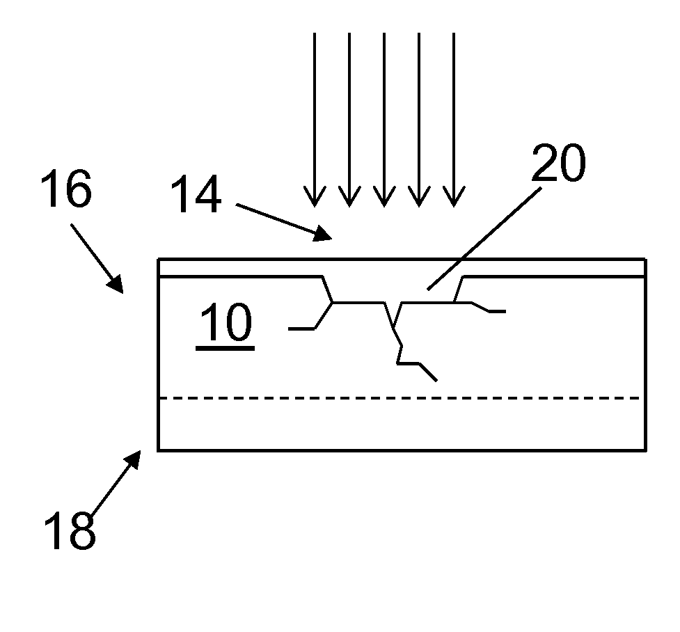
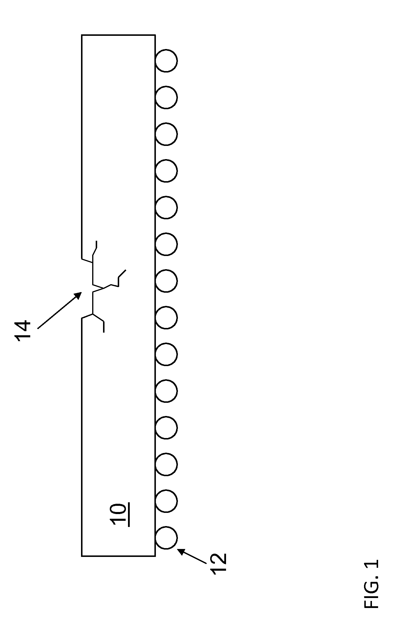
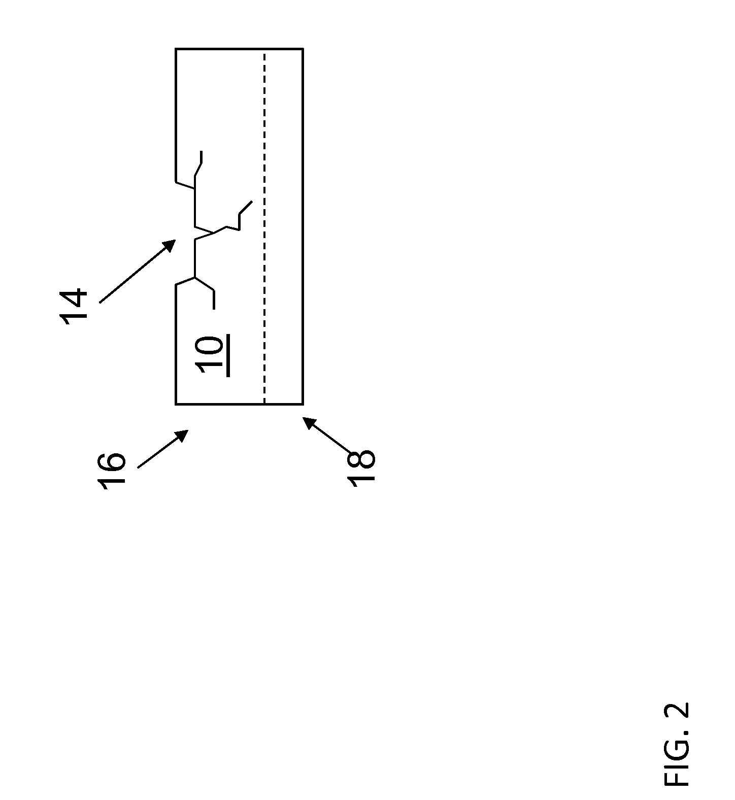
Stiff quantum layers to slow and or stop defect propagation
PatentInactiveUS10861939B2
Innovation
- Incorporating elastically stiff quantum regions within the epitaxial material to prevent or redirect defect propagation, using materials with higher elastic stiffness and similar lattice parameters to the epitaxial material, often in thin layers to minimize self-induced defects.


Inhibiting propagation of imperfections in semiconductor devices
PatentInactiveUS20140042594A1
Innovation
- A method involving screening for surface imperfections on silicon wafers and depositing an organic epoxy material to adhere adjacent surfaces together, preventing the propagation of imperfections into the active region of the wafer.

Environmental Standards for Semiconductor Manufacturing
Environmental standards in semiconductor manufacturing have evolved into comprehensive frameworks that directly impact defect propagation control across production cycles. These standards encompass cleanroom classifications, contamination control protocols, and atmospheric management systems that collectively minimize particle introduction and chemical impurities during fabrication processes.
The ISO 14644 series establishes fundamental cleanroom standards, defining particle concentration limits and monitoring requirements that prevent external contamination sources from introducing defects into semiconductor wafers. Class 1 cleanrooms, commonly used in advanced node production, maintain particle counts below 10 particles per cubic meter for particles 0.1 micrometers and larger, significantly reducing the probability of defect initiation.
Chemical purity standards, particularly SEMI specifications, govern the quality of process gases, chemicals, and ultrapure water used throughout manufacturing. These standards mandate impurity levels in the parts-per-billion range for critical materials, preventing ionic contamination that can propagate as electrical defects across multiple production lots. Regular monitoring and certification ensure consistent material quality that breaks defect propagation chains.
Atmospheric control standards address humidity, temperature, and molecular contamination management within fabrication facilities. Maintaining relative humidity below 45% and temperature stability within ±0.1°C prevents moisture-related defects and thermal stress variations that can compound across production cycles. Molecular filtration systems remove organic and acidic vapors that otherwise accumulate on wafer surfaces.
Waste management and emission control standards complement contamination prevention by establishing protocols for chemical disposal, exhaust treatment, and facility maintenance. These standards prevent cross-contamination between production areas and ensure that cleaning and maintenance activities do not introduce new defect sources into subsequent manufacturing cycles.
Recent updates to environmental standards increasingly focus on real-time monitoring capabilities and predictive contamination control, enabling proactive defect prevention rather than reactive responses. Advanced sensor networks and data analytics integration allow manufacturers to identify environmental deviations before they manifest as propagating defects across production batches.
Supply Chain Risk Management in Semiconductor Production
Supply chain risk management in semiconductor production represents a critical operational framework that directly impacts defect propagation patterns across manufacturing cycles. The semiconductor industry's complex global supply network creates multiple vulnerability points where material inconsistencies, supplier quality variations, and logistical disruptions can introduce defect-causing factors into production streams. Effective risk management strategies must address both upstream supplier reliability and downstream manufacturing consistency to minimize defect transmission throughout production cycles.
Raw material quality control constitutes the primary defense against defect propagation in semiconductor manufacturing. Silicon wafer suppliers, chemical precursor providers, and specialty gas manufacturers must maintain stringent quality standards to prevent contamination sources from entering the production chain. Supply chain risk assessment protocols typically evaluate supplier certification levels, quality management systems, and historical performance metrics to identify potential defect introduction points. Advanced supplier qualification programs now incorporate real-time monitoring systems that track material purity levels, delivery consistency, and batch-to-batch variations that could contribute to downstream defect formation.
Geographic diversification strategies play an essential role in mitigating supply chain risks that could amplify defect propagation. Single-source dependencies create vulnerability scenarios where supplier disruptions can force manufacturers to accept lower-quality alternatives, potentially introducing new defect mechanisms into established production processes. Multi-sourcing approaches, while increasing complexity, provide risk mitigation by enabling rapid supplier switching when quality issues emerge. Regional supply chain mapping helps identify concentration risks where multiple suppliers share common infrastructure or raw material sources.
Inventory management practices significantly influence defect propagation control within semiconductor production environments. Just-in-time delivery systems, while cost-effective, can create pressure to accept marginal-quality materials when supply disruptions occur. Strategic buffer inventory policies for critical materials provide flexibility to reject substandard supplies without production interruptions. Advanced inventory tracking systems now incorporate material genealogy capabilities that enable rapid identification and isolation of defective material batches before they propagate through multiple production cycles.
Supplier relationship management frameworks increasingly emphasize collaborative defect prevention rather than reactive quality control. Joint development programs with key suppliers focus on understanding how material properties influence downstream defect formation patterns. Shared quality metrics and real-time data exchange enable proactive identification of emerging quality trends before they manifest as production defects. Long-term partnership agreements often include provisions for joint investment in quality improvement initiatives and defect reduction technologies.
Emergency response protocols for supply chain disruptions must balance production continuity with defect prevention objectives. Qualification procedures for alternative suppliers require accelerated testing methodologies that can quickly assess defect risk potential without compromising production schedules. Pre-qualified backup supplier networks provide rapid response capabilities while maintaining quality standards that prevent defect introduction during crisis situations.
Unlock deeper insights with PatSnap Eureka Quick Research — get a full tech report to explore trends and direct your research. Try now!
Generate Your Research Report Instantly with AI Agent
Supercharge your innovation with PatSnap Eureka AI Agent Platform!