

Enhancing Photolithography Process Stability In Variable Environments
FEB 24, 20269 MIN READ
Generate Your Research Report Instantly with AI Agent
PatSnap Eureka helps you evaluate technical feasibility & market potential.
Photolithography Stability Background and Technical Objectives
Photolithography stands as the cornerstone of modern semiconductor manufacturing, enabling the precise patterning of integrated circuits at nanometer scales. Since its inception in the 1960s, this technology has evolved from contact printing to advanced extreme ultraviolet lithography, continuously pushing the boundaries of Moore's Law. The fundamental principle involves transferring circuit patterns from photomasks onto silicon wafers through light exposure and chemical processing. However, as feature sizes shrink below 7nm nodes, the process has become increasingly sensitive to environmental variations, threatening yield rates and manufacturing consistency.
Environmental fluctuations present critical challenges to photolithography stability. Temperature variations affect resist viscosity, exposure dose requirements, and overlay accuracy. Humidity changes impact resist adhesion and development uniformity. Atmospheric pressure fluctuations alter air refractive indices, affecting optical path lengths in exposure systems. Vibrations from facility operations introduce alignment errors. These variables compound at advanced nodes where tolerances measured in single-digit nanometers leave minimal margin for error. The semiconductor industry faces mounting pressure to maintain process stability across diverse manufacturing environments, from established fabs to emerging production facilities in different geographical regions.
The primary technical objective centers on developing robust methodologies and control systems that ensure photolithography process consistency despite environmental perturbations. This encompasses real-time monitoring and compensation mechanisms for temperature, humidity, and pressure variations. Advanced metrology integration aims to provide immediate feedback for dynamic process adjustments. Machine learning algorithms are being explored to predict and preemptively correct environmental impacts before they affect production outcomes.
Secondary objectives include establishing standardized environmental control protocols adaptable to different facility infrastructures, reducing dependency on costly cleanroom specifications, and enabling flexible manufacturing capabilities. The ultimate goal involves achieving sub-nanometer overlay accuracy and critical dimension uniformity across variable conditions, thereby improving yield rates, reducing production costs, and accelerating time-to-market for next-generation semiconductor devices. Success in these objectives will determine competitive advantage in an increasingly demanding global semiconductor landscape.
Market Demand for Advanced Lithography Solutions
The semiconductor industry is experiencing unprecedented demand for advanced lithography solutions driven by the relentless pursuit of smaller node geometries and higher device densities. As manufacturers transition toward sub-5nm process nodes and prepare for the 3nm and 2nm generations, the requirements for photolithography equipment have become increasingly stringent. This technological progression necessitates lithography systems capable of maintaining exceptional process stability across varying environmental conditions, as even minor fluctuations can result in critical dimension variations that compromise yield and device performance.
The proliferation of artificial intelligence, high-performance computing, and 5G infrastructure has intensified the demand for advanced semiconductor devices with superior performance characteristics. These applications require chips manufactured with extreme precision, where photolithography process stability directly impacts product quality and manufacturing economics. Foundries and integrated device manufacturers are actively seeking solutions that can minimize process variations caused by environmental factors such as temperature fluctuations, humidity changes, atmospheric pressure variations, and vibration disturbances.
Market dynamics reveal a growing emphasis on total cost of ownership reduction through improved process control and yield enhancement. Manufacturers recognize that unstable lithography processes lead to increased scrap rates, extended development cycles, and reduced production throughput. The economic impact of process instability becomes particularly significant at advanced nodes where wafer costs are substantially higher and profit margins are compressed. Consequently, there is strong market pull for lithography technologies and methodologies that can deliver consistent results despite environmental variability.
The expansion of semiconductor manufacturing into geographically diverse regions with varying climatic conditions has further amplified the need for robust lithography solutions. New fabrication facilities in different continents face distinct environmental challenges, from tropical humidity to continental temperature extremes. This geographical diversification creates demand for lithography systems and process control strategies that can maintain performance consistency across diverse operational environments without requiring extensive facility modifications.
Additionally, the emergence of heterogeneous integration and advanced packaging technologies has created new lithography application scenarios beyond traditional wafer processing. These applications often occur in environments with less stringent controls than cleanroom facilities, necessitating lithography solutions with inherent resilience to environmental variations. The market increasingly values technologies that can bridge the gap between laboratory-grade precision and real-world manufacturing conditions.
Current Challenges in Variable Environment Lithography
Photolithography in semiconductor manufacturing faces significant stability challenges when operating under variable environmental conditions. Temperature fluctuations represent one of the most critical factors affecting process consistency. Even minor variations of 0.1°C can cause thermal expansion in optical components and wafer stages, leading to overlay errors and critical dimension variations. The refractive index of immersion fluids and lens materials also exhibits temperature sensitivity, directly impacting the focal plane positioning and resolution uniformity across the exposure field.
Atmospheric pressure and humidity variations introduce additional complexity to the lithography process. Changes in air pressure alter the refractive index of the optical path, causing focus drift and aberrations in the projection system. Humidity fluctuations affect photoresist properties, particularly its sensitivity and development characteristics, resulting in inconsistent pattern transfer. These environmental parameters become increasingly problematic as feature sizes shrink below 7nm nodes, where tolerances are measured in single-digit nanometers.
Vibration and acoustic disturbances from facility operations pose substantial threats to exposure accuracy. External vibrations from nearby equipment, building movements, or transportation activities can exceed the sub-nanometer stability requirements of advanced lithography tools. These mechanical disturbances directly translate into overlay errors and pattern placement inaccuracies, particularly during the extended exposure times required for extreme ultraviolet lithography systems.
Chemical contamination and airborne molecular contaminants present persistent challenges in maintaining process stability. Trace amounts of organic compounds, acids, or bases in the cleanroom environment can interact with photoresist materials, causing unpredictable changes in sensitivity and contrast. The accumulation of particulates on optical surfaces degrades transmission efficiency and introduces localized defects that compromise pattern fidelity.
The integration of multiple environmental control systems creates interdependencies that complicate stability management. Heating, ventilation, and air conditioning systems must coordinate with precision temperature control units while maintaining cleanroom classification standards. Any imbalance in these systems can trigger cascading effects that destabilize multiple process parameters simultaneously, making root cause analysis and corrective actions increasingly difficult.
Existing Environmental Compensation Solutions
01 Process monitoring and control systems for photolithography
Advanced monitoring and control systems are implemented to maintain process stability in photolithography. These systems utilize real-time feedback mechanisms, sensors, and automated adjustments to ensure consistent exposure conditions, temperature control, and alignment accuracy. By continuously monitoring critical parameters and making dynamic corrections, these systems help maintain uniform pattern transfer and reduce process variations across wafer batches.- Process monitoring and control systems for photolithography: Advanced monitoring and control systems can be implemented to enhance photolithography process stability. These systems utilize real-time data acquisition and feedback mechanisms to detect process variations and make automatic adjustments. Sensors and metrology tools continuously monitor critical parameters such as exposure dose, focus, and overlay accuracy. The collected data is analyzed to identify deviations from target specifications, enabling immediate corrective actions. This approach minimizes process drift and ensures consistent pattern transfer across multiple wafers and production runs.
- Temperature and environmental control in photolithography chambers: Maintaining stable temperature and environmental conditions within photolithography equipment is critical for process stability. Precise control of ambient temperature, humidity, and air pressure prevents variations in photoresist properties and exposure characteristics. Advanced thermal management systems regulate the temperature of critical components including the wafer stage, reticle, and optical elements. Environmental control systems filter airborne particles and maintain cleanroom conditions to prevent contamination. These measures reduce process variability caused by environmental fluctuations and ensure reproducible lithographic results.
- Photoresist material optimization and coating uniformity: The selection and application of photoresist materials significantly impact photolithography process stability. Advanced photoresist formulations with improved thermal stability and reduced sensitivity to environmental variations enhance process robustness. Precise coating techniques ensure uniform photoresist thickness across the wafer surface, minimizing pattern distortion and critical dimension variations. Post-application bake processes are carefully controlled to achieve consistent photoresist properties. Material characterization and quality control procedures verify photoresist performance before processing, reducing batch-to-batch variations.
- Optical system calibration and maintenance: Regular calibration and maintenance of optical systems are essential for maintaining photolithography process stability. Precision alignment of optical elements ensures accurate pattern projection and minimizes aberrations. Laser source stability monitoring and adjustment maintain consistent exposure energy throughout production runs. Lens cleaning and contamination prevention procedures preserve optical performance over time. Automated calibration routines verify and correct focus, overlay, and dose parameters before each production lot. These practices prevent gradual degradation of lithographic performance and maintain tight process control.
- Statistical process control and defect reduction strategies: Implementation of statistical process control methodologies enhances photolithography process stability by identifying and eliminating sources of variation. Data from multiple process steps is collected and analyzed to detect trends and anomalies before they impact product quality. Advanced pattern recognition algorithms identify defect signatures and correlate them with specific process conditions. Predictive maintenance schedules based on equipment performance data prevent unexpected failures. Root cause analysis of process excursions leads to systematic improvements in process capability and yield enhancement.
02 Overlay and alignment accuracy improvement
Maintaining precise overlay and alignment between successive lithography layers is critical for process stability. Techniques include advanced metrology systems, alignment mark optimization, and compensation algorithms that account for wafer distortion and thermal expansion. These methods ensure that patterns are accurately positioned relative to previous layers, reducing defects and improving yield consistency throughout the manufacturing process.Expand Specific Solutions03 Photoresist process optimization and uniformity control
Achieving stable photoresist coating, exposure, and development processes is essential for lithography stability. This involves optimizing spin coating parameters, bake temperatures and times, and development conditions to ensure uniform film thickness and consistent pattern resolution. Process control techniques also address edge bead removal and defect reduction to maintain high-quality pattern transfer across entire wafers.Expand Specific Solutions04 Environmental control and contamination management
Photolithography process stability heavily depends on maintaining controlled environmental conditions including temperature, humidity, and air quality. Contamination from particles, chemical vapors, or moisture can significantly impact pattern fidelity and process repeatability. Advanced cleanroom technologies, filtration systems, and environmental monitoring ensure that external factors do not introduce variability into the lithography process.Expand Specific Solutions05 Exposure dose control and optical system stability
Precise control of exposure dose and maintaining optical system stability are fundamental to photolithography process consistency. This includes laser power stabilization, illumination uniformity optimization, and lens aberration correction. Advanced calibration methods and periodic maintenance of optical components ensure that the exposure energy delivered to the photoresist remains constant, resulting in reproducible critical dimensions and pattern profiles across production runs.Expand Specific Solutions
Major Players in Semiconductor Lithography Equipment
The photolithography process stability enhancement field represents a mature yet rapidly evolving sector within semiconductor manufacturing, driven by increasing demands for precision in advanced node production. The market is dominated by established equipment manufacturers like ASML Netherlands BV and ASML Holding NV, who lead in EUV lithography technology, alongside Canon and Nikon in traditional lithography systems. Technology maturity varies significantly across players: ASML demonstrates highest advancement in EUV systems enabling sub-7nm processes, while Tokyo Electron, Applied Materials, and Synopsys contribute through complementary process equipment and design automation solutions. Foundry operators including GLOBALFOUNDRIES, SMIC-Beijing, and Shanghai Huali Microelectronics drive practical implementation requirements. The competitive landscape shows consolidation around few equipment leaders, with emerging Chinese players like Shanghai Microelectronics Equipment attempting to develop domestic capabilities, indicating a market transitioning toward geographically diversified supply chains while maintaining high technological barriers to entry.
ASML Netherlands BV
Technical Solution: ASML has developed advanced environmental control systems for their extreme ultraviolet (EUV) and deep ultraviolet (DUV) lithography equipment to maintain process stability across variable conditions. Their technology incorporates real-time temperature compensation mechanisms, atmospheric pressure monitoring systems, and vibration isolation platforms that actively adjust to environmental fluctuations[1][4]. The company implements sophisticated thermal management solutions including precision cooling systems that maintain wafer and reticle temperatures within ±0.01°C tolerances. Additionally, ASML's overlay correction algorithms continuously compensate for environmental drift by utilizing advanced metrology feedback loops and predictive modeling to adjust exposure parameters dynamically, ensuring consistent pattern fidelity even when ambient conditions vary[2][5].
Strengths: Industry-leading precision control, comprehensive environmental monitoring, proven track record in high-volume manufacturing. Weaknesses: High system complexity, significant capital investment required, dependency on specialized maintenance expertise[3][6].
Canon, Inc.
Technical Solution: Canon has developed comprehensive environmental adaptation technologies for their nanoimprint and optical lithography systems, emphasizing modular environmental control architectures. Their approach includes isolated environmental chambers with independent temperature, humidity, and pressure control zones that can be individually optimized for different process steps[13][15]. Canon's systems feature adaptive optical correction mechanisms that utilize real-time wavefront sensing to compensate for thermally-induced aberrations in variable temperature environments. The company has pioneered the use of machine learning algorithms to predict environmental impact patterns and automatically adjust process parameters including exposure dose, focus offset, and overlay corrections. Their environmental buffering technology creates stable micro-environments around critical components while allowing flexibility in fab-level conditions[14][16].
Strengths: Innovative nanoimprint technology, flexible modular design, strong machine learning integration for predictive control. Weaknesses: Limited market presence in advanced nodes, smaller installed base for data collection compared to market leaders[17][18].
Core Patents in Lithography Stability Enhancement
Optical proximity correction (OPC) technique using generalized figure of merit for photolithograhic processing
PatentInactiveUS6978438B1
Innovation
- A method and program for making optical proximity corrections using a generalized figure of merit (GFOM) that manipulates edge segments of reticle layouts to account for optical distortions, generating individual figure of merit values and a weighted GFOM to optimize reticle layouts, incorporating edge placement error, image contrast, depth of focus, and fragmentation complexity, to improve image fidelity and tolerance to process variations.


Method for determining lithographic focus and exposure
PatentInactiveUS20080192221A1
Innovation
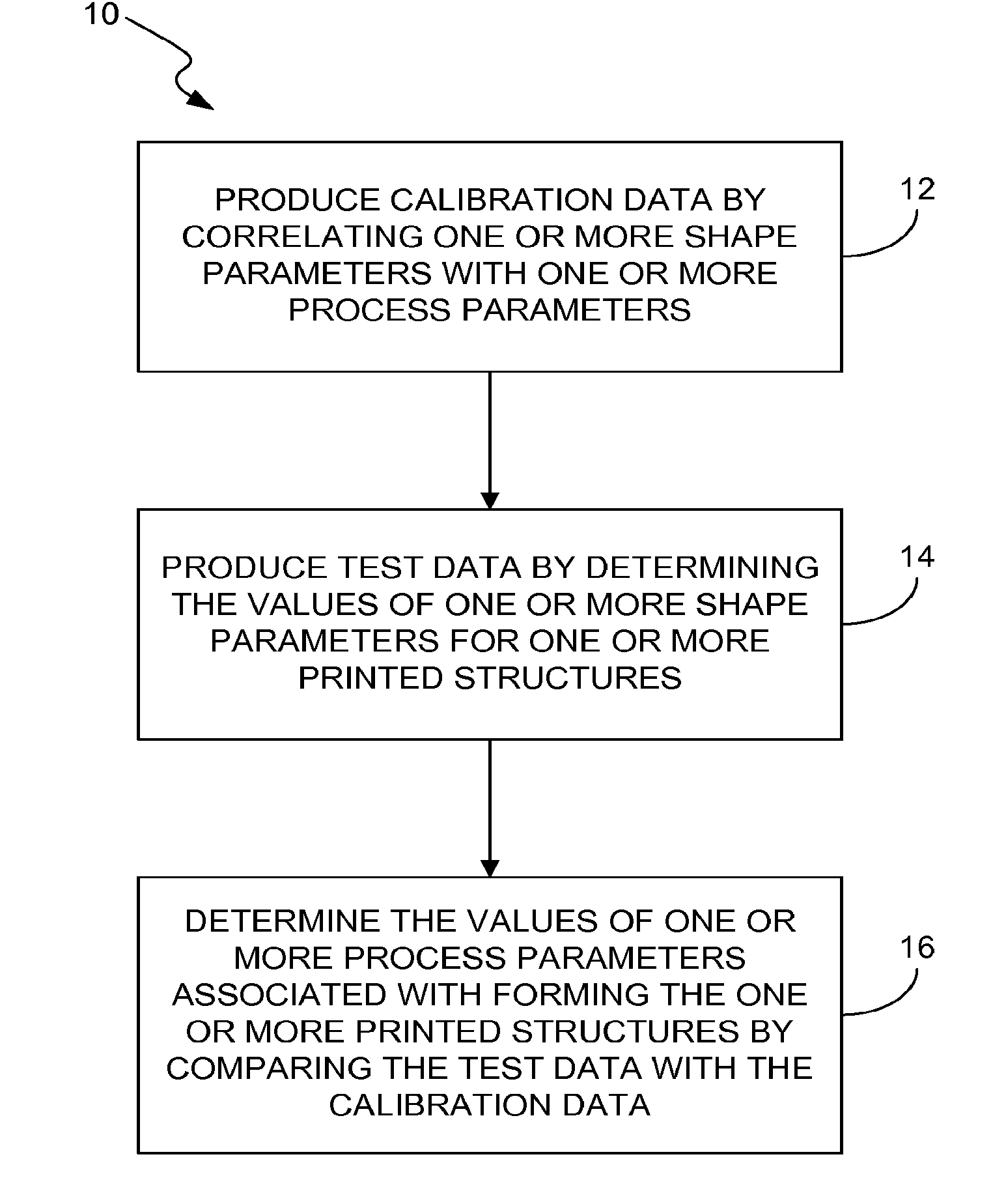
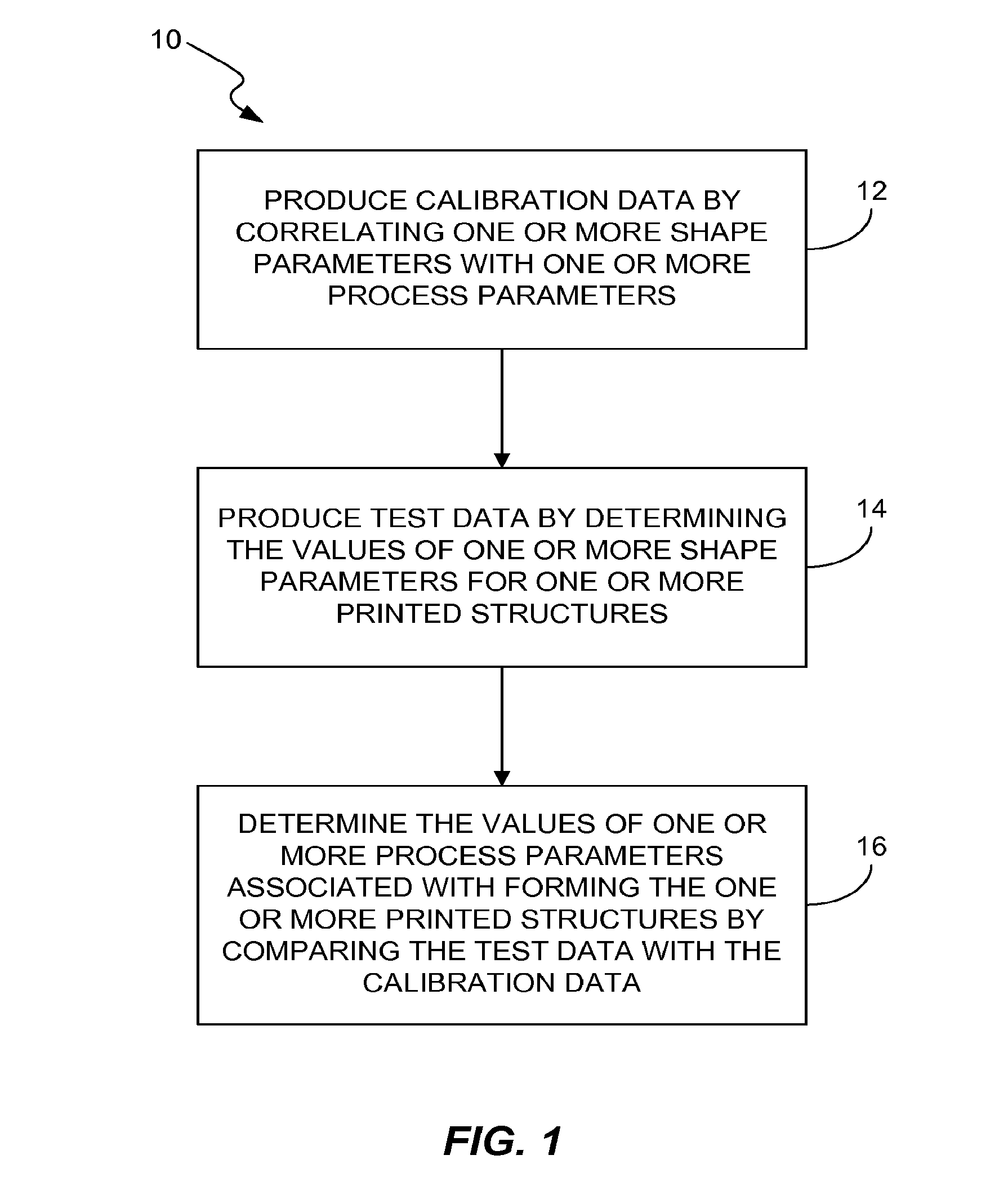
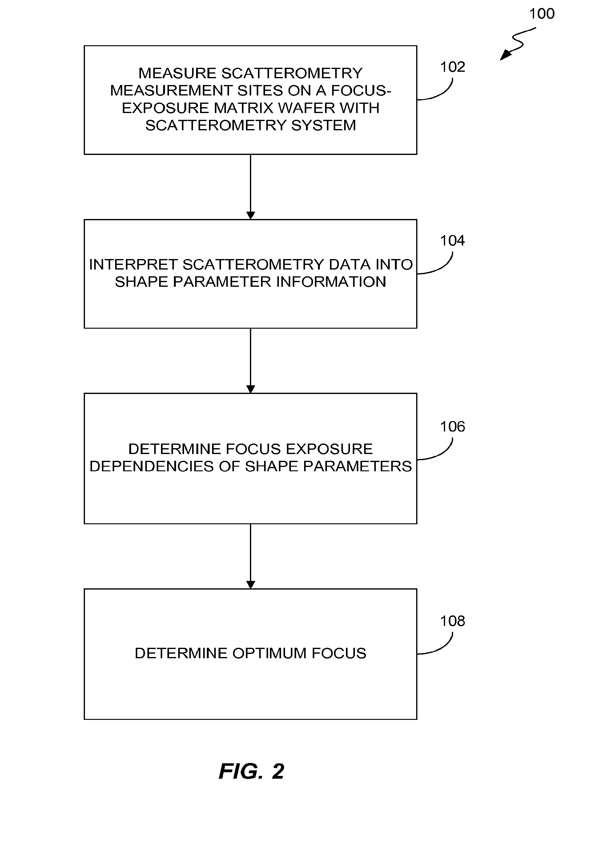
- A method using scatterometry measurements to correlate shape parameters with process parameters, allowing for simultaneous determination of focus and exposure settings on production wafers without stopping production, by interpreting scatterometry data into shape parameter information and matching it with focus exposure dependencies to determine optimal processing conditions.

Cleanroom Standards and Environmental Regulations
Photolithography process stability in semiconductor manufacturing is fundamentally governed by stringent cleanroom standards and environmental regulations that define the operational boundaries for achieving consistent nanoscale patterning. The International Organization for Standardization (ISO) 14644 series establishes the classification framework for cleanroom environments, with modern photolithography facilities typically operating at ISO Class 1 to Class 4 levels, where particle concentrations are maintained below 10 particles per cubic meter for particles sized 0.1 micrometers and larger. These standards directly impact process stability by minimizing contamination-induced defects that can compromise pattern fidelity and yield rates.
Temperature and humidity control represent critical regulatory parameters, with industry standards typically requiring temperature stability within ±0.1°C and relative humidity control at 45±2% for advanced lithography processes. The Federal Standard 209E and its successor ISO 14644 mandate continuous monitoring and documentation of environmental parameters, establishing traceability requirements that enable correlation between environmental fluctuations and process variations. Compliance with these standards necessitates sophisticated HVAC systems capable of maintaining uniform airflow patterns, typically employing unidirectional flow at velocities between 0.3 to 0.5 meters per second to ensure effective particle removal.
Regional regulatory frameworks further influence cleanroom design and operation, with the European Union's Good Manufacturing Practice (GMP) guidelines and the United States' FDA regulations imposing additional requirements for pharmaceutical and medical device applications that increasingly intersect with semiconductor manufacturing. Environmental regulations concerning chemical handling, particularly for photoresists and developers, mandate specific ventilation rates and containment protocols that affect facility design and operational procedures.
Emerging regulations addressing energy efficiency and environmental sustainability are reshaping cleanroom operations, with standards such as LEED certification and ISO 50001 energy management systems driving adoption of advanced filtration technologies and energy recovery systems. These evolving requirements challenge facilities to maintain process stability while reducing environmental footprint, necessitating innovative approaches to environmental control that balance regulatory compliance with operational efficiency and process consistency in variable manufacturing conditions.
Cost-Benefit Analysis of Stability Enhancement Technologies
Implementing stability enhancement technologies in photolithography processes requires careful evaluation of financial implications against anticipated performance improvements. The initial capital investment varies significantly across different technological approaches, ranging from environmental control systems to advanced metrology equipment and adaptive process control algorithms. Active thermal management systems typically demand substantial upfront costs between $500,000 to $2 million per production line, while atmospheric pressure and humidity control infrastructure may require $1-3 million depending on cleanroom specifications. Advanced overlay correction systems and real-time monitoring solutions represent additional investments of $800,000 to $1.5 million per scanner tool.
Operational expenditure considerations extend beyond initial procurement costs. Enhanced environmental control systems increase energy consumption by approximately 15-25%, translating to annual utility cost increases of $200,000-400,000 per facility. Maintenance requirements for sophisticated monitoring equipment and control systems add recurring costs of 8-12% of capital investment annually. However, these expenses must be weighed against significant operational benefits, including reduced defect rates, improved yield performance, and decreased rework requirements.
The economic benefits manifest through multiple channels. Enhanced process stability typically delivers yield improvements of 3-8% in advanced node production, representing substantial revenue gains given wafer values exceeding $10,000 for leading-edge processes. Reduced process variability minimizes scrap rates and rework cycles, saving approximately $1.5-3 million annually per production line. Improved overlay accuracy and critical dimension control extend equipment utilization periods and reduce unscheduled downtime by 20-30%, enhancing overall equipment effectiveness.
Return on investment calculations demonstrate favorable outcomes for most stability enhancement technologies, with payback periods ranging from 18 to 36 months depending on production volumes and technology nodes. High-volume manufacturing facilities processing advanced nodes below 7nm typically achieve faster ROI due to higher wafer values and tighter process margins. The cumulative financial benefit over a five-year period often exceeds 200-300% of initial investment when accounting for yield improvements, reduced waste, and enhanced production capacity utilization.
Unlock deeper insights with PatSnap Eureka Quick Research — get a full tech report to explore trends and direct your research. Try now!
Generate Your Research Report Instantly with AI Agent
Supercharge your innovation with PatSnap Eureka AI Agent Platform!