

Improving Photolithography Throughput Using Stepper Adjustments
FEB 24, 20268 MIN READ
Generate Your Research Report Instantly with AI Agent
PatSnap Eureka helps you evaluate technical feasibility & market potential.
Photolithography Throughput Enhancement Background and Objectives
Photolithography stands as the cornerstone technology in semiconductor manufacturing, enabling the transfer of intricate circuit patterns onto silicon wafers through precise light exposure and chemical processing. Since its inception in the 1960s, this technology has evolved from contact printing to projection lithography, and subsequently to advanced immersion lithography and extreme ultraviolet systems. Each evolutionary leap has been driven by the relentless pursuit of smaller feature sizes and higher manufacturing efficiency to meet the exponential growth demands outlined by Moore's Law.
The semiconductor industry faces mounting pressure to increase production capacity while maintaining cost-effectiveness and quality standards. As chip complexity escalates and market demand surges, particularly for applications in artificial intelligence, 5G communications, and automotive electronics, manufacturers must optimize every aspect of the fabrication process. Photolithography typically accounts for 30-40% of total wafer processing time, making it a critical bottleneck in overall manufacturing throughput.
Stepper technology, which employs a step-and-repeat exposure method to pattern wafers, represents a significant portion of installed lithography equipment worldwide. Unlike scanners that expose patterns through continuous motion, steppers offer advantages in certain applications including lower equipment costs and simpler maintenance requirements. However, their inherent operational characteristics present unique opportunities for throughput optimization through systematic adjustments to exposure parameters, stage movement algorithms, and process integration strategies.
The primary objective of this research focuses on identifying and implementing stepper adjustment methodologies that can substantially enhance photolithography throughput without compromising pattern fidelity or overlay accuracy. This encompasses optimizing exposure dose strategies, refining wafer stage acceleration profiles, improving focus control mechanisms, and streamlining reticle handling procedures. Secondary objectives include reducing operational costs per wafer, extending equipment uptime, and establishing scalable optimization frameworks applicable across different stepper platforms and technology nodes. Achieving these goals will enable semiconductor manufacturers to maximize return on existing capital investments while meeting aggressive production targets in an increasingly competitive global market.
Market Demand for High-Volume Semiconductor Manufacturing
The semiconductor industry is experiencing unprecedented demand driven by the proliferation of advanced technologies across multiple sectors. High-volume manufacturing capabilities have become critical as applications in artificial intelligence, 5G communications, automotive electronics, and Internet of Things devices continue to expand rapidly. This surge in demand has placed immense pressure on fabrication facilities to maximize production efficiency while maintaining stringent quality standards.
Photolithography represents the most critical and expensive bottleneck in semiconductor manufacturing processes, accounting for a substantial portion of both capital expenditure and production cycle time. As chip designs become increasingly complex with smaller feature sizes and higher layer counts, the number of lithography steps per wafer has grown significantly. This trend has intensified the need for enhanced throughput without compromising pattern fidelity or overlay accuracy.
The economic implications of photolithography throughput are substantial for semiconductor manufacturers. Extended exposure times and lengthy wafer handling processes directly impact fab utilization rates and overall equipment effectiveness. With lithography tools representing multi-million dollar investments and operating costs, even marginal improvements in throughput can translate to significant competitive advantages and improved return on investment.
Market dynamics are further complicated by the ongoing capacity constraints in leading-edge and mature node production. Foundries and integrated device manufacturers are seeking solutions that can increase output from existing equipment installations rather than solely relying on capital-intensive capacity expansion. This creates strong demand for optimization strategies that leverage stepper adjustments and process refinements to extract maximum performance from current lithography assets.
The competitive landscape in high-volume manufacturing increasingly favors organizations that can achieve superior cycle times while maintaining yield targets. Customers across consumer electronics, data center infrastructure, and automotive sectors are demanding shorter lead times and greater supply chain responsiveness. Consequently, manufacturers are actively pursuing technologies and methodologies that enhance photolithography throughput as a strategic imperative for market positioning and customer satisfaction.
Current Stepper Technology Status and Bottlenecks
Photolithography steppers represent the cornerstone of modern semiconductor manufacturing, enabling the precise patterning of integrated circuits on silicon wafers. Current stepper technology has evolved significantly from early contact and proximity aligners to sophisticated step-and-repeat systems capable of sub-10nm resolution. Leading platforms incorporate advanced optical systems with deep ultraviolet (DUV) light sources operating at 193nm wavelength, complemented by immersion lithography techniques that achieve numerical apertures exceeding 1.35. Extreme ultraviolet (EUV) lithography at 13.5nm wavelength has emerged as the frontier technology, though its adoption remains limited by equipment cost and operational complexity.
Despite remarkable technological achievements, contemporary stepper systems face critical throughput constraints that directly impact manufacturing economics. The fundamental bottleneck lies in the sequential nature of wafer processing, where each exposure field requires precise alignment, focusing, and exposure cycles. Modern steppers typically achieve throughput rates between 150 to 275 wafers per hour for DUV systems, while EUV systems operate at significantly lower rates of 125 to 160 wafers per hour due to limited source power and extended exposure times.
Stage movement and positioning accuracy present another substantial challenge. High-precision wafer stages must achieve nanometer-level positioning accuracy while maintaining rapid acceleration and deceleration cycles. The mechanical settling time required after each stage movement to eliminate vibrations and ensure measurement stability consumes approximately 15-25% of total cycle time. This overhead becomes increasingly problematic as feature sizes shrink and overlay requirements tighten to below 2nm for advanced nodes.
Overlay measurement and correction procedures constitute additional throughput impediments. Current systems employ sophisticated metrology subsystems that measure alignment marks before each exposure, with measurement times ranging from 0.3 to 0.8 seconds per mark. Multi-patterning techniques required for advanced technology nodes necessitate multiple lithography steps with stringent overlay control, exponentially increasing the cumulative metrology burden and reducing effective throughput.
Thermal management issues further constrain operational efficiency. Continuous laser exposure generates substantial heat loads that cause lens element distortion and wafer thermal expansion, necessitating periodic cooling intervals and real-time correction systems. These thermal effects become more pronounced in high-volume manufacturing environments, forcing throughput reductions to maintain process stability and yield targets.
Existing Stepper Optimization Solutions
01 Wafer stage and reticle stage optimization for increased throughput
Improving the speed and accuracy of wafer and reticle stage movements can significantly enhance stepper throughput. This includes implementing advanced stage control systems, dual-stage configurations, and optimized acceleration/deceleration profiles to minimize settling time and increase the number of wafers processed per hour. Enhanced positioning systems and feedback mechanisms ensure precise alignment while maintaining high-speed operation.- Wafer stage and reticle stage optimization for increased throughput: Improving the speed and accuracy of wafer and reticle stage movements can significantly enhance stepper throughput. This includes implementing advanced stage control systems, dual-stage configurations, and optimized acceleration/deceleration profiles to minimize settling time and increase the number of wafers processed per hour. Enhanced positioning systems and feedback mechanisms ensure precise alignment while maintaining high-speed operation.
- Advanced alignment and overlay measurement systems: Implementing high-speed alignment systems and real-time overlay measurement techniques can reduce the time required for wafer positioning and pattern alignment. These systems utilize sophisticated optical sensors, image processing algorithms, and predictive alignment methods to achieve accurate positioning with minimal measurement time, thereby increasing overall throughput without compromising alignment accuracy.
- Exposure system and illumination optimization: Optimizing the exposure system through improved illumination sources, enhanced optical systems, and advanced exposure control methods can increase throughput. This includes using high-intensity light sources, optimized pupil configurations, and parallel exposure techniques to reduce exposure time per field while maintaining pattern quality and resolution requirements.
- Automated wafer handling and transport systems: Implementing efficient wafer handling mechanisms, including robotic transfer systems, automated loading/unloading systems, and optimized wafer flow paths can minimize non-productive time. Advanced scheduling algorithms and buffer management systems ensure continuous operation and reduce idle time between wafer exchanges, significantly improving overall equipment efficiency and throughput.
- Process control and predictive maintenance for throughput optimization: Utilizing advanced process control systems, real-time monitoring, and predictive maintenance strategies can maximize stepper uptime and throughput. These systems employ sensors, data analytics, and machine learning algorithms to detect potential issues before they cause downtime, optimize process parameters dynamically, and schedule maintenance activities to minimize impact on production throughput.
02 Advanced alignment and overlay measurement systems
Implementing high-speed alignment systems and real-time overlay measurement techniques can reduce the time required for wafer positioning and pattern alignment. These systems utilize advanced optical sensors, image processing algorithms, and predictive alignment methods to achieve accurate positioning with minimal measurement time, thereby increasing overall throughput without compromising alignment accuracy.Expand Specific Solutions03 Exposure system and illumination optimization
Optimizing the exposure system through improved illumination sources, enhanced optical systems, and advanced exposure control methods can increase throughput. This includes using high-intensity light sources, optimized pupil configurations, and parallel exposure techniques to reduce exposure time per field while maintaining pattern quality and resolution requirements.Expand Specific Solutions04 Automated wafer handling and transport systems
Implementing efficient wafer handling mechanisms, including robotic transfer systems, automated loading/unloading systems, and optimized wafer flow paths can minimize non-productive time. Advanced scheduling algorithms and buffer management systems ensure continuous operation and reduce idle time between wafer exchanges, significantly improving overall equipment efficiency and throughput.Expand Specific Solutions05 Process control and predictive maintenance for throughput optimization
Utilizing advanced process control systems, real-time monitoring, and predictive maintenance strategies can maximize stepper uptime and throughput. These systems employ sensors, data analytics, and machine learning algorithms to detect potential issues before they cause downtime, optimize process parameters dynamically, and schedule maintenance activities to minimize impact on production throughput.Expand Specific Solutions
Major Lithography Equipment Manufacturers Analysis
The photolithography throughput improvement landscape represents a mature yet rapidly evolving sector within the semiconductor manufacturing industry, driven by escalating demand for advanced chips and increasing production complexity. The market demonstrates substantial growth potential as manufacturers face mounting pressure to enhance efficiency while managing rising costs. Technology maturity varies significantly across players, with ASML Netherlands BV dominating advanced EUV lithography systems, while Nikon Corp. and Canon Inc. maintain positions in DUV stepper technologies. Leading semiconductor manufacturers including Intel Corp., Micron Technology, SK hynix, and TSMC-affiliated entities like Shanghai Huali Microelectronics and Semiconductor Manufacturing International demonstrate sophisticated implementation capabilities. Chinese players such as Shanghai Microelectronics Equipment and Dongfang Jingyuan Electron are advancing domestic capabilities, while equipment specialists like Litel Instruments provide critical metrology solutions. The competitive landscape reflects a technology race between established Western leaders and emerging Asian manufacturers, with stepper adjustment optimization becoming increasingly critical for next-generation node production efficiency.
ASML Netherlands BV
Technical Solution: ASML has developed advanced stepper and scanner systems with sophisticated throughput optimization technologies. Their systems incorporate dynamic focus and leveling adjustments that enable real-time wafer stage positioning corrections during exposure, reducing alignment time by up to 30%. The company's Twinscan platform utilizes dual-stage architecture where one wafer is being exposed while another is simultaneously being measured and aligned, effectively doubling throughput capacity. ASML's overlay control systems employ advanced algorithms for predictive maintenance and automatic recipe optimization, which minimize downtime and maximize wafer-per-hour output. Their latest generation systems achieve throughput rates exceeding 275 wafers per hour for advanced nodes through optimized stage acceleration profiles and reduced settling times.
Strengths: Industry-leading throughput performance with dual-stage architecture, superior overlay accuracy enabling faster processing, extensive installed base providing rich operational data for optimization. Weaknesses: Extremely high capital costs limiting accessibility, complex systems requiring specialized maintenance expertise, long lead times for equipment delivery and installation.
Nikon Corp.
Technical Solution: Nikon has implemented throughput enhancement solutions in their NSR-S series steppers through optimized stage control algorithms and advanced reticle handling systems. Their approach focuses on minimizing non-productive time by improving wafer exchange mechanisms and reducing alignment measurement cycles. Nikon's systems feature adaptive exposure control that adjusts illumination parameters dynamically based on real-time feedback, maintaining quality while maximizing speed. The company has developed proprietary stage synchronization technology that reduces settling time between exposure fields by approximately 20-25%. Their throughput optimization includes predictive scheduling algorithms that optimize the sequence of wafer processing to minimize stage travel distance and acceleration/deceleration cycles, achieving throughput improvements of 15-20% compared to baseline configurations.
Strengths: Cost-effective solutions compared to competitors, proven reliability in mature node production, strong integration with existing fab infrastructure. Weaknesses: Lower market share in advanced nodes limiting R&D resources, throughput performance gaps versus leading competitors at cutting-edge nodes, reduced ecosystem support compared to market leaders.
Core Patents in Stepper Throughput Enhancement
Method of identifying bottlenecks and improving throughput in wafer processing equipment
PatentInactiveUS6856847B2
Innovation
- A method using the theory of constraints to determine segmental processing times and identify bottlenecks by calculating throughput based on the number of tool units in each segment, allowing for targeted process improvements.


Lithography stepper alignment and control method
PatentActiveUS20170192363A1
Innovation
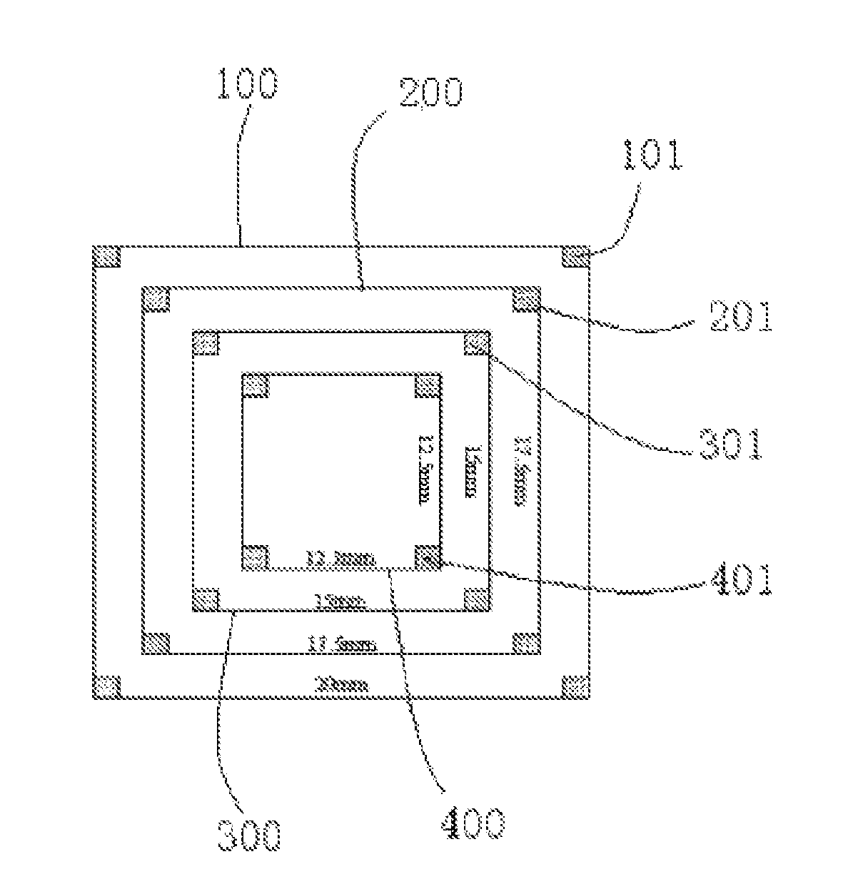
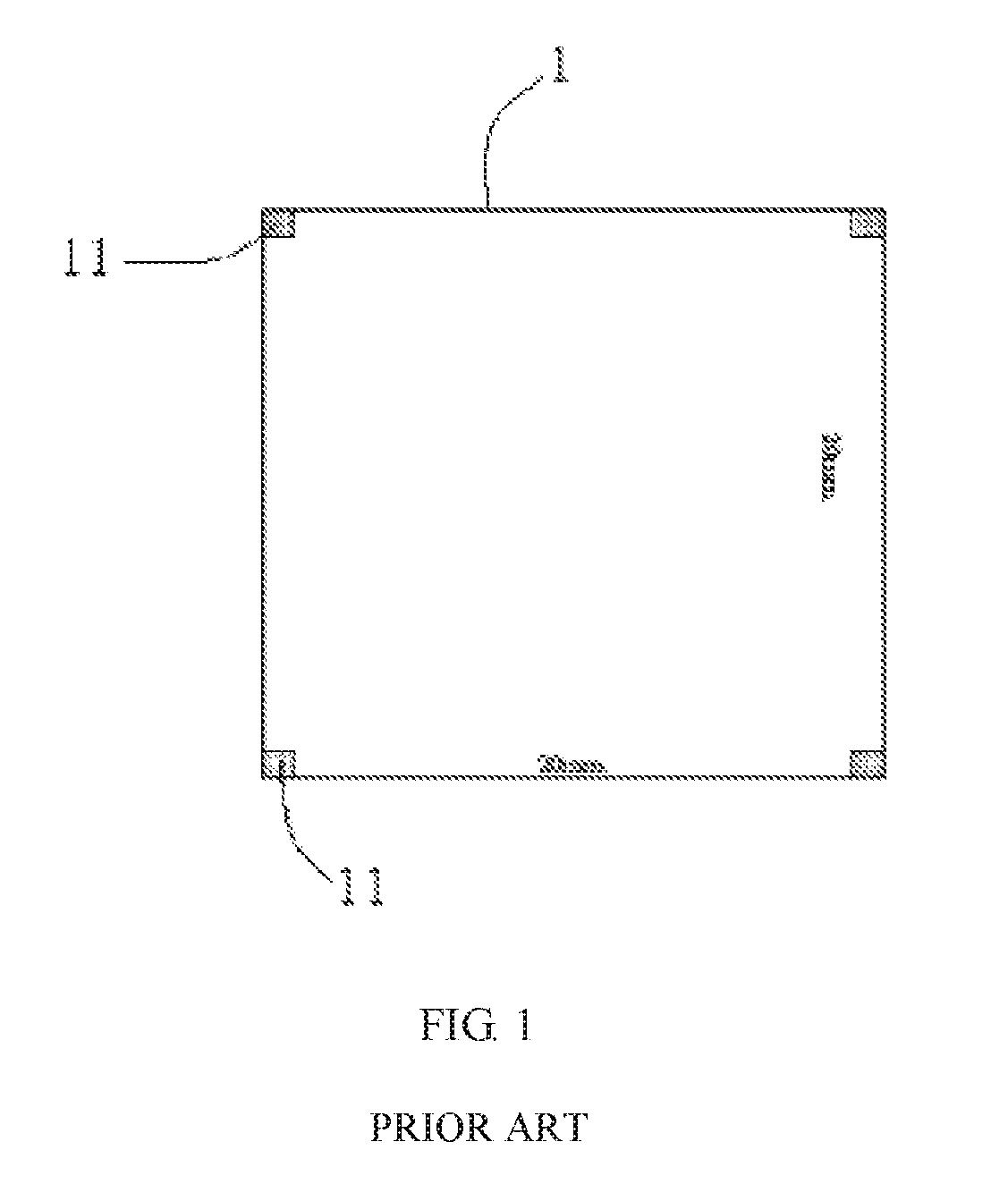
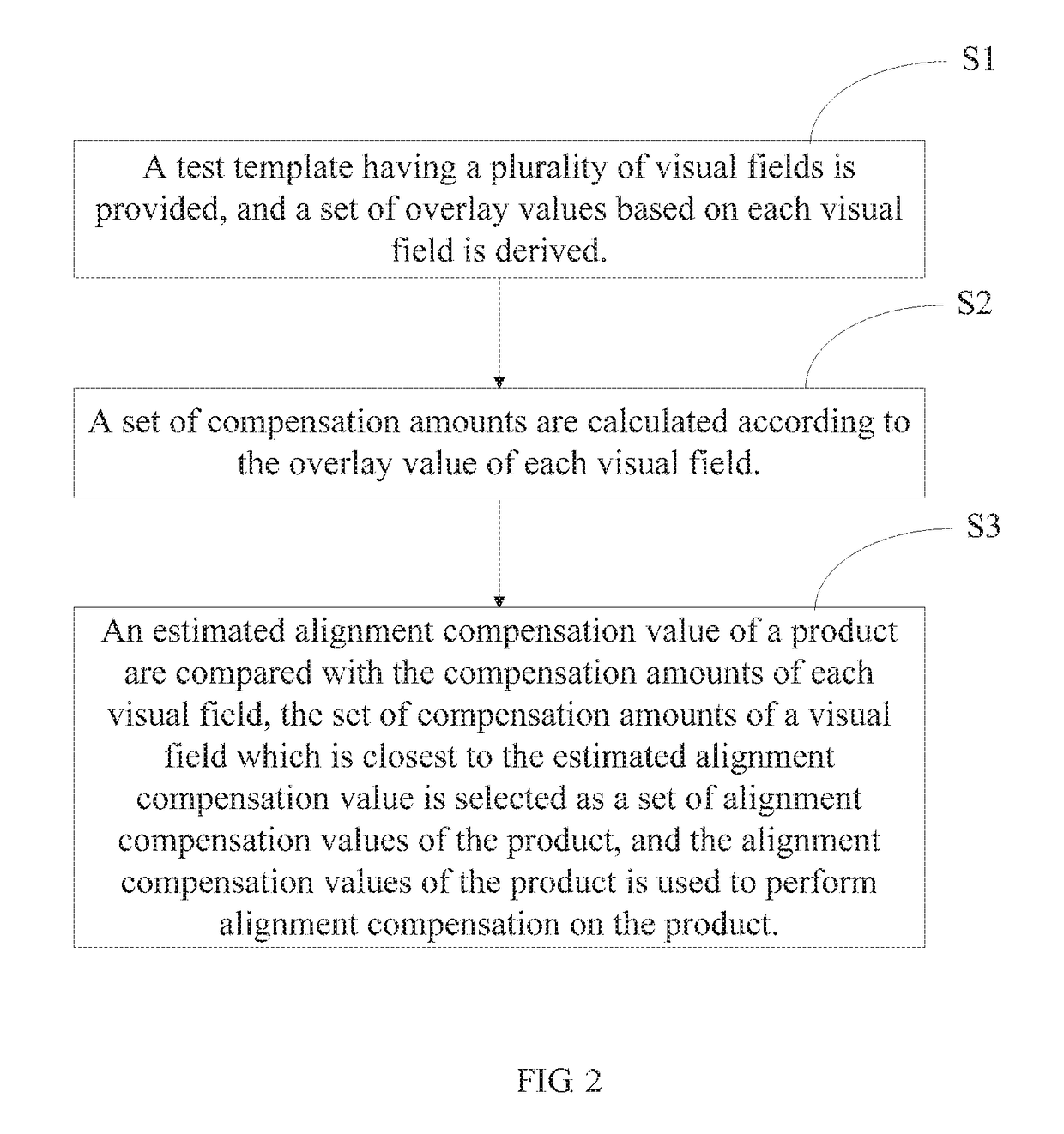
- A method involving a test template with multiple visual fields to derive and compare overlay values, selecting compensation amounts closest to the product's visual field for accurate alignment compensation, reducing the likelihood of misalignment and improving control without increasing costs or manpower.

Cost-Benefit Analysis of Throughput Improvement
Evaluating the economic viability of throughput enhancement through stepper adjustments requires a comprehensive examination of both capital expenditures and operational returns. Initial investments typically encompass hardware modifications, advanced control systems, and precision calibration equipment. These upfront costs must be weighed against the projected increase in wafer processing capacity, which directly translates to higher production volumes and revenue generation potential. The payback period for such investments generally ranges from eighteen to thirty-six months, depending on facility utilization rates and product mix complexity.
Operational cost considerations extend beyond initial capital outlays to include maintenance expenses, energy consumption variations, and potential yield impacts during optimization phases. Enhanced throughput often demands more frequent preventive maintenance cycles and specialized technical support, which incrementally increases operational budgets. However, these costs are typically offset by reduced per-wafer processing expenses as fixed overhead is distributed across larger production volumes. Energy efficiency improvements through optimized stage movements and reduced idle times can contribute additional savings of five to eight percent in facility operating costs.
The revenue enhancement potential stems from multiple sources including accelerated time-to-market for new products, improved asset utilization, and enhanced competitive positioning. Facilities achieving throughput improvements of fifteen to twenty-five percent can accommodate additional customer orders without capacity expansion, effectively increasing return on existing assets. This operational leverage becomes particularly valuable during high-demand periods when premium pricing opportunities emerge. Furthermore, demonstrated capability in high-volume production strengthens customer relationships and facilitates long-term contract negotiations.
Risk mitigation strategies must account for potential implementation challenges including temporary production disruptions, learning curve effects, and technology obsolescence concerns. Phased implementation approaches that validate improvements on selected equipment before full-scale deployment help minimize operational risks while building organizational confidence. Sensitivity analyses considering various demand scenarios and competitive responses provide essential decision-making frameworks for investment justification and resource allocation priorities.
Integration with Advanced Process Nodes
As semiconductor manufacturing advances toward smaller feature sizes, the integration of stepper adjustment strategies with advanced process nodes becomes increasingly critical for maintaining high throughput without compromising yield. At the 5nm node and beyond, the tolerance margins for overlay accuracy, focus control, and dose uniformity shrink dramatically, requiring stepper systems to operate within extremely narrow process windows. Traditional throughput optimization methods must now account for the heightened sensitivity of advanced lithography processes to even minor variations in stepper performance parameters.
The transition to extreme ultraviolet lithography for critical layers introduces additional complexity to stepper adjustment protocols. EUV systems demand precise synchronization between source power stability, reticle heating compensation, and wafer stage positioning to maintain throughput targets. Stepper adjustments must accommodate the unique characteristics of EUV resist chemistry, which exhibits different response curves compared to deep ultraviolet materials. This necessitates recalibration of exposure dose strategies and development of adaptive control algorithms that can respond to real-time process variations while sustaining production rates.
Multi-patterning techniques employed at advanced nodes further complicate the relationship between stepper adjustments and throughput optimization. Self-aligned quadruple patterning and other decomposition methods require multiple lithography steps with stringent overlay requirements between successive exposures. Stepper adjustment strategies must balance the need for enhanced accuracy across these sequential steps against the cumulative impact on cycle time. Advanced metrology integration and feed-forward correction mechanisms become essential to prevent throughput degradation while meeting the overlay budgets demanded by sub-7nm manufacturing.
The implementation of high numerical aperture EUV systems represents the next frontier in this integration challenge. These systems introduce new variables such as anamorphic optics and increased sensitivity to lens heating effects, requiring novel approaches to stepper adjustment that preserve throughput gains. Process engineers must develop holistic optimization frameworks that consider the interdependencies between stepper parameters, advanced node requirements, and production efficiency metrics to achieve sustainable manufacturing performance at the technology frontier.
Unlock deeper insights with PatSnap Eureka Quick Research — get a full tech report to explore trends and direct your research. Try now!
Generate Your Research Report Instantly with AI Agent
Supercharge your innovation with PatSnap Eureka AI Agent Platform!