

Semiconductor Structural Integrity Under Vibration
MAR 31, 20269 MIN READ
Generate Your Research Report Instantly with AI Agent
PatSnap Eureka helps you evaluate technical feasibility & market potential.
Semiconductor Vibration Challenges and Structural Goals
The semiconductor industry faces unprecedented challenges as electronic devices become increasingly compact while operating in more demanding environments. Vibration-induced failures represent a critical threat to semiconductor structural integrity, particularly in automotive, aerospace, and mobile applications where devices experience continuous mechanical stress. These challenges stem from the fundamental mismatch between the brittle nature of semiconductor materials and the dynamic loading conditions they encounter during operation.
Modern semiconductor packages incorporate multiple materials with vastly different thermal expansion coefficients and mechanical properties, creating inherent stress concentrations at interfaces. Silicon dies, copper interconnects, polymer substrates, and ceramic components each respond differently to vibrational forces, leading to complex stress distributions that can initiate crack propagation and eventual failure. The miniaturization trend exacerbates these issues by reducing the cross-sectional areas available to distribute mechanical loads.
Current vibration-related failure modes include solder joint fatigue, wire bond degradation, die cracking, and delamination at material interfaces. These failures often manifest as intermittent electrical connections, increased resistance, or complete circuit interruption. The challenge is compounded by the fact that vibration-induced damage can accumulate over extended periods, making early detection and prevention strategies essential for reliable operation.
The primary technical goal is to develop comprehensive methodologies for predicting and preventing vibration-induced failures in semiconductor devices. This encompasses establishing robust design guidelines that account for dynamic loading conditions, developing advanced materials with improved mechanical properties, and creating innovative packaging architectures that effectively isolate sensitive components from external vibrations.
Another critical objective involves developing standardized testing protocols that accurately simulate real-world vibration environments while providing reproducible results for design validation. These protocols must address the wide frequency spectrum encountered in various applications, from low-frequency automotive vibrations to high-frequency aerospace conditions.
The ultimate goal is achieving semiconductor devices capable of maintaining structural and electrical integrity throughout their operational lifetime, even under severe vibrational stress. This requires integrating mechanical design principles with traditional semiconductor engineering approaches, creating a new paradigm for robust electronic system development that ensures reliability across diverse and challenging operating environments.
Market Demand for Vibration-Resistant Semiconductor Devices
The global semiconductor industry faces mounting pressure to develop vibration-resistant devices as applications expand into increasingly demanding environments. Traditional semiconductor packaging and design approaches, originally developed for stable desktop and server environments, prove inadequate for modern deployment scenarios where mechanical stress and vibrational forces are prevalent.
Automotive electronics represents the largest and fastest-growing market segment driving demand for vibration-resistant semiconductors. Modern vehicles contain hundreds of semiconductor devices that must withstand engine vibrations, road-induced mechanical stress, and thermal cycling throughout operational lifespans exceeding fifteen years. Advanced driver assistance systems, electric vehicle power management units, and autonomous driving processors require exceptional structural integrity while maintaining precise electrical performance under continuous vibrational stress.
Aerospace and defense applications constitute another critical market segment with stringent reliability requirements. Satellite systems, aircraft avionics, and military equipment operate in extreme vibrational environments where semiconductor failure can result in mission-critical consequences. These applications demand specialized packaging technologies, enhanced die attachment methods, and robust interconnect solutions that maintain electrical integrity under severe mechanical stress conditions.
Industrial automation and robotics sectors increasingly rely on semiconductor devices capable of withstanding repetitive mechanical forces. Manufacturing equipment, robotic systems, and industrial sensors operate in environments with continuous vibrations from motors, actuators, and mechanical processes. The growing adoption of Industry 4.0 technologies amplifies demand for reliable semiconductor solutions that maintain performance accuracy despite mechanical disturbances.
Consumer electronics markets drive volume demand for cost-effective vibration-resistant solutions. Smartphones, tablets, wearable devices, and gaming systems require semiconductors that survive repeated drops, impacts, and handling stresses while maintaining functionality. The proliferation of portable devices with advanced processing capabilities necessitates innovative packaging approaches that balance mechanical robustness with miniaturization requirements.
Emerging applications in renewable energy systems, particularly wind turbines and solar tracking mechanisms, create additional market opportunities. These installations subject semiconductor components to prolonged vibrational stress from environmental factors and mechanical operations, requiring enhanced structural integrity solutions that ensure long-term reliability in harsh outdoor conditions.
Current State and Challenges of Semiconductor Vibration Tolerance
The semiconductor industry has made significant strides in developing vibration-resistant packaging and design methodologies over the past two decades. Current state-of-the-art approaches primarily focus on mechanical reinforcement through advanced packaging materials, including low-stress molding compounds and flexible substrates that can absorb vibrational energy. Leading manufacturers have implemented sophisticated finite element analysis tools to predict stress distributions and failure modes under various vibrational conditions.
Modern semiconductor devices demonstrate varying degrees of vibration tolerance depending on their structural configuration and application requirements. Consumer electronics typically withstand vibrations up to 20G acceleration levels, while automotive and aerospace applications demand tolerance levels exceeding 50G. Current packaging technologies such as chip-scale packages (CSP) and system-in-package (SiP) configurations have shown improved resilience compared to traditional dual in-line packages, primarily due to reduced mechanical leverage and enhanced structural integrity.
Despite these advances, several critical challenges persist in achieving optimal vibration tolerance. Wire bonding remains a primary failure point, with bond wire fatigue and heel cracking occurring under prolonged vibrational stress. The mismatch in thermal expansion coefficients between different materials within semiconductor packages creates additional stress concentrations that are exacerbated by vibrational loading. Solder joint reliability continues to be problematic, particularly in ball grid array configurations where repeated mechanical stress leads to crack propagation and eventual electrical failure.
Emerging challenges include the miniaturization trend that demands thinner die and finer pitch interconnects, inherently reducing mechanical robustness. High-frequency vibrations, particularly those above 1000 Hz, pose unique challenges as they can induce resonance effects in package structures, leading to amplified stress levels and accelerated failure mechanisms. The integration of heterogeneous materials in advanced packaging solutions introduces complex stress interaction patterns that are difficult to predict and mitigate.
Current testing methodologies, while comprehensive, often fail to accurately replicate real-world vibrational environments. Standard vibration tests typically employ sinusoidal or random vibration profiles that may not capture the complex multi-axial and transient vibrations encountered in actual applications. This gap between laboratory testing and field conditions represents a significant challenge in developing truly robust semiconductor solutions for demanding vibrational environments.
Existing Solutions for Semiconductor Vibration Protection
01 Stress management and mechanical reinforcement structures
Semiconductor devices require careful management of mechanical stress to maintain structural integrity. Various reinforcement structures, including support layers, stress-relief patterns, and mechanical buffer zones, can be incorporated into semiconductor designs to prevent cracking, delamination, and warping during manufacturing and operation. These structures help distribute stress more evenly across the device and accommodate thermal expansion mismatches between different materials.- Structural reinforcement through protective layers and coatings: Semiconductor devices can be protected through the application of specialized protective layers and coatings that enhance structural integrity. These layers serve as barriers against mechanical stress, environmental factors, and chemical degradation. Various materials and deposition techniques can be employed to create robust protective structures that maintain the physical stability of semiconductor components throughout their operational lifetime.
- Stress management and mechanical reinforcement structures: Managing internal and external stress in semiconductor structures is critical for maintaining integrity. This involves implementing mechanical reinforcement structures, stress-relief patterns, and optimized geometries that distribute forces evenly across the device. Techniques include the use of buffer layers, strategic placement of support structures, and design modifications that accommodate thermal expansion and contraction without compromising structural stability.
- Bonding and interconnection integrity enhancement: The structural integrity of semiconductor devices heavily depends on the quality and reliability of bonding and interconnection methods. Advanced bonding techniques, improved adhesion materials, and optimized interconnection designs ensure that different layers and components remain securely attached under various operating conditions. These methods address issues such as delamination, interface failure, and connection degradation that can compromise device performance.
- Defect detection and structural monitoring systems: Maintaining semiconductor structural integrity requires effective detection and monitoring of defects and structural anomalies. Advanced inspection techniques, real-time monitoring systems, and non-destructive testing methods enable early identification of cracks, voids, delamination, and other structural defects. These systems utilize various technologies to assess the physical condition of semiconductor structures and predict potential failure points before they become critical.
- Packaging and encapsulation for structural protection: Proper packaging and encapsulation techniques are essential for preserving semiconductor structural integrity against external threats. These methods involve selecting appropriate encapsulation materials, optimizing package designs, and implementing sealing techniques that protect semiconductor devices from moisture, contaminants, and physical damage. The packaging approach must balance protection requirements with thermal management and electrical performance considerations.
02 Encapsulation and protective coating technologies
Protective encapsulation layers and coatings are essential for maintaining semiconductor structural integrity by shielding devices from environmental factors such as moisture, contaminants, and mechanical damage. Advanced encapsulation materials and techniques provide hermetic sealing while maintaining electrical performance. These protective measures prevent corrosion, reduce stress concentration points, and enhance overall device reliability and longevity.Expand Specific Solutions03 Interconnect and bonding integrity enhancement
The structural integrity of semiconductor devices heavily depends on the reliability of interconnections and bonding interfaces. Advanced bonding techniques, improved adhesion layers, and optimized interconnect designs help prevent delamination, void formation, and mechanical failure at critical junctions. These methods ensure robust electrical connections while maintaining mechanical stability under thermal cycling and operational stress conditions.Expand Specific Solutions04 Defect detection and structural monitoring methods
Maintaining semiconductor structural integrity requires effective detection and monitoring of defects, cracks, and structural anomalies. Various inspection techniques and monitoring systems can identify potential failure points during manufacturing and operation. These methods enable early detection of structural weaknesses, allowing for corrective measures before catastrophic failure occurs and ensuring consistent device quality and reliability.Expand Specific Solutions05 Thermal management and dimensional stability
Effective thermal management is critical for semiconductor structural integrity as temperature fluctuations can cause dimensional changes, thermal stress, and material degradation. Design strategies incorporating heat dissipation structures, thermal interface materials, and coefficient of thermal expansion matching help maintain dimensional stability. These approaches minimize thermally-induced mechanical stress and prevent structural failure due to repeated thermal cycling during device operation.Expand Specific Solutions
Key Players in Semiconductor and Vibration Testing Industry
The semiconductor structural integrity under vibration research field represents an emerging yet critical technology domain driven by increasing miniaturization demands and harsh operating environments in automotive, aerospace, and IoT applications. The market demonstrates significant growth potential as reliability requirements intensify across industries. Technology maturity varies considerably among key players, with established foundries like Taiwan Semiconductor Manufacturing Co. and SMIC leading in advanced process nodes and structural optimization, while memory specialists including ChangXin Memory Technologies and Yangtze Memory Technologies focus on vibration-resistant storage solutions. Equipment manufacturers such as Applied Materials and Tokyo Electron provide essential testing and fabrication tools, whereas companies like Hitachi and Renesas Electronics integrate vibration-resistant designs into automotive and industrial applications, indicating a fragmented but rapidly evolving competitive landscape.
Taiwan Semiconductor Manufacturing Co., Ltd.
Technical Solution: TSMC has developed advanced packaging technologies including CoWoS (Chip-on-Wafer-on-Substrate) and InFO (Integrated Fan-Out) that incorporate comprehensive vibration resistance design. Their approach utilizes multi-layer stress buffer structures and optimized underfill materials to enhance structural integrity under mechanical stress. The company employs finite element analysis (FEA) modeling to predict vibration response and implements specialized bonding techniques that can withstand automotive-grade vibration requirements up to 20G acceleration. Their advanced node processes (3nm/5nm) integrate mechanical reliability considerations from the design phase, ensuring semiconductor devices maintain electrical performance under various vibration conditions through improved interconnect structures and substrate engineering.
Strengths: Industry-leading advanced packaging technology with proven automotive-grade reliability standards. Weaknesses: High cost implementation and complex manufacturing processes requiring specialized equipment.
Applied Materials, Inc.
Technical Solution: Applied Materials focuses on equipment-level solutions for semiconductor structural integrity, developing specialized deposition and etching systems that create more robust device structures. Their approach includes advanced chemical vapor deposition (CVD) systems that produce high-quality stress-engineered films and specialized annealing processes that optimize material properties for vibration resistance. The company's Endura platform incorporates real-time stress monitoring during manufacturing, enabling precise control of film stress to minimize structural vulnerabilities. Their solutions include specialized metrology tools that can measure mechanical properties at the nanoscale level, ensuring semiconductor devices meet stringent vibration specifications for aerospace and automotive applications through improved material uniformity and reduced defect density.
Strengths: Comprehensive equipment solutions with integrated process control and advanced metrology capabilities. Weaknesses: Focus primarily on manufacturing equipment rather than device-level design solutions.
Core Innovations in Semiconductor Structural Integrity
Method and apparatus for determining material structural integrity
PatentInactiveUS5520052A
Innovation
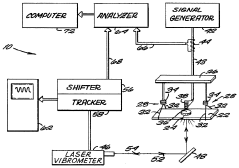
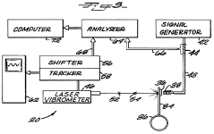
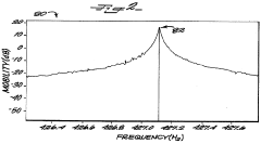
- Combining laser vibrometry with damping analysis techniques to measure the damping loss factor of materials over a known frequency range, allowing for the determination of structural integrity through the use of vibrational force and velocity measurements, and plotting drive point mobility to derive the damping loss factor.
Structural integrity monitoring system
PatentInactiveUS20100269592A1
Innovation
- A structural integrity monitoring system with at least two vibration monitoring devices and a controller that calculates a predicted vibration response based on mode shapes and compares it to measured responses to detect changes in the structure, allowing for real-time monitoring and differentiation between load-induced and deterioration-induced vibrations.


Reliability Standards for Semiconductor Vibration Testing
The semiconductor industry has established comprehensive reliability standards for vibration testing to ensure device performance and longevity under mechanical stress conditions. These standards provide systematic frameworks for evaluating structural integrity and operational reliability of semiconductor components across various application environments.
International standards organizations have developed multiple testing protocols, with JEDEC (Joint Electron Device Engineering Council) leading the semiconductor-specific guidelines through standards such as JESD22-B103 for mechanical shock and JESD22-B104 for vibration testing. These standards define specific test conditions, frequency ranges, acceleration levels, and duration requirements tailored to different semiconductor package types and application scenarios.
Military and aerospace applications follow more stringent standards, including MIL-STD-883 and MIL-STD-202, which specify enhanced vibration testing procedures for components operating in harsh environments. These standards typically require higher acceleration levels, extended frequency sweeps, and multiple-axis testing to simulate extreme operational conditions encountered in defense and space applications.
Automotive semiconductor reliability standards, particularly AEC-Q100 for integrated circuits and AEC-Q101 for discrete semiconductors, incorporate vibration testing requirements specific to automotive environments. These standards address the unique challenges of temperature cycling combined with mechanical vibration, reflecting real-world automotive operating conditions where components experience simultaneous thermal and mechanical stresses.
Consumer electronics standards, including IEC 60068-2-6 and ASTM D999, provide guidelines for vibration testing of semiconductor devices in portable and stationary consumer products. These standards emphasize testing protocols that simulate handling, transportation, and operational vibrations typical in consumer applications, with particular attention to handheld devices and mobile electronics.
The evolution of packaging technologies has driven updates to existing standards and development of new testing protocols. Advanced packaging formats such as system-in-package (SiP), 3D stacked devices, and flexible electronics require specialized vibration testing approaches that address unique structural vulnerabilities and failure modes not covered by traditional standards.
Compliance with these reliability standards ensures semiconductor manufacturers can validate their products' mechanical robustness, establish quality benchmarks, and provide customers with confidence in device performance under specified vibration conditions across diverse application environments.
Environmental Impact of Semiconductor Manufacturing Processes
Semiconductor manufacturing processes generate significant environmental impacts across multiple dimensions, creating complex challenges that intersect with structural integrity considerations under vibrational stress. The production of semiconductor devices involves extensive use of hazardous chemicals, ultra-pure water, and energy-intensive processes that collectively contribute to substantial environmental footprints.
Chemical emissions represent one of the most critical environmental concerns in semiconductor fabrication. Manufacturing facilities utilize thousands of different chemicals including acids, solvents, dopants, and cleaning agents. Many of these substances are classified as volatile organic compounds (VOCs), greenhouse gases, or toxic air pollutants. Perfluorinated compounds (PFCs) used in plasma etching and chamber cleaning processes possess extremely high global warming potentials, sometimes exceeding 10,000 times that of carbon dioxide.
Water consumption and wastewater generation constitute another major environmental challenge. Semiconductor fabs require enormous quantities of ultra-pure water for wafer cleaning, rinsing, and cooling operations. A typical 300mm wafer fabrication facility consumes approximately 2,000-4,000 gallons of water per minute. The resulting wastewater contains various contaminants including heavy metals, organic solvents, and acidic or basic solutions that require extensive treatment before discharge.
Energy consumption in semiconductor manufacturing is exceptionally high due to the need for maintaining cleanroom environments, operating sophisticated equipment, and supporting continuous production cycles. The industry's carbon footprint continues expanding as demand for semiconductors grows exponentially, particularly with emerging technologies like artificial intelligence and 5G communications driving increased chip complexity and production volumes.
Solid waste generation includes spent chemicals, contaminated materials, packaging waste, and defective wafers. Many of these materials require specialized disposal methods due to their hazardous nature. Silicon wafer scraps, while recyclable, often contain trace amounts of dopants or processing residues that complicate recycling efforts.
The environmental impact extends to resource depletion, particularly rare earth elements and precious metals used in semiconductor manufacturing. Mining and processing these materials create additional environmental burdens including habitat destruction, soil contamination, and water pollution in extraction regions.
Regulatory frameworks worldwide are increasingly stringent regarding semiconductor manufacturing emissions. The industry faces mounting pressure to adopt sustainable practices, implement circular economy principles, and develop environmentally friendly alternatives to traditional manufacturing processes while maintaining the precision and reliability required for advanced semiconductor devices.
Unlock deeper insights with PatSnap Eureka Quick Research — get a full tech report to explore trends and direct your research. Try now!
Generate Your Research Report Instantly with AI Agent
Supercharge your innovation with PatSnap Eureka AI Agent Platform!