Semiconductor Wafer Bonding for 3D Integration Applications
MAR 31, 20269 MIN READ
Generate Your Research Report Instantly with AI Agent
Patsnap Eureka helps you evaluate technical feasibility & market potential.
Wafer Bonding Technology Background and 3D Integration Goals
Semiconductor wafer bonding technology has emerged as a critical enablement technique for three-dimensional integrated circuits, representing a paradigm shift from traditional planar scaling approaches. The technology traces its origins to the early 1980s when researchers first explored direct wafer bonding for silicon-on-insulator applications. Initially developed for MEMS devices and optical applications, wafer bonding has evolved significantly to address the growing demands of advanced semiconductor manufacturing.
The fundamental principle of wafer bonding involves creating permanent adhesion between two or more semiconductor wafers through various physical and chemical mechanisms. Early implementations focused primarily on hydrophilic and hydrophobic direct bonding, where surface preparation and cleaning protocols determined bond quality. As the technology matured, additional bonding methods emerged, including anodic bonding, thermocompression bonding, and adhesive-based approaches, each offering distinct advantages for specific applications.
The evolution toward 3D integration applications gained momentum in the late 1990s and early 2000s as Moore's Law scaling became increasingly challenging and expensive. Traditional two-dimensional scaling faced fundamental physical limitations, including quantum effects, power density constraints, and interconnect delays. Industry leaders recognized that vertical integration offered a viable path to continue performance improvements while managing manufacturing costs and power consumption.
Modern 3D integration goals encompass multiple strategic objectives that address contemporary semiconductor challenges. Performance enhancement represents a primary driver, as vertical stacking reduces interconnect lengths between functional blocks, thereby minimizing signal propagation delays and improving overall system speed. This architectural approach enables heterogeneous integration, allowing different process technologies and materials to be combined within a single package.
Power efficiency constitutes another critical objective, as shorter interconnects reduce parasitic capacitances and resistances, leading to lower dynamic power consumption. Additionally, 3D architectures enable more efficient thermal management strategies and voltage domain partitioning, further optimizing power performance characteristics.
Form factor reduction drives significant market adoption, particularly in mobile and wearable applications where space constraints are paramount. Vertical integration allows manufacturers to achieve higher functionality density while maintaining or reducing package footprints, enabling more compact and lightweight electronic devices.
The technology also targets cost optimization through improved silicon utilization efficiency and reduced package complexity. By enabling heterogeneous integration, manufacturers can optimize each functional layer using the most appropriate process technology, potentially reducing overall manufacturing costs while improving yield and performance characteristics.
Market Demand for 3D Semiconductor Integration Solutions
The semiconductor industry is experiencing unprecedented demand for 3D integration solutions driven by the relentless pursuit of higher performance, increased functionality, and miniaturization across multiple application domains. Traditional planar scaling approaches are reaching physical and economic limitations, creating substantial market pressure for innovative three-dimensional architectures that can deliver enhanced performance within constrained form factors.
Mobile computing devices represent the largest demand driver for 3D semiconductor integration technologies. Smartphones, tablets, and wearable devices require increasingly sophisticated processing capabilities while maintaining strict power consumption and thermal management constraints. The integration of multiple functional layers through advanced wafer bonding techniques enables manufacturers to achieve higher transistor densities and improved interconnect efficiency, directly addressing market requirements for enhanced computational performance in compact designs.
Data center and high-performance computing applications constitute another significant demand segment for 3D integration solutions. Cloud computing infrastructure, artificial intelligence accelerators, and machine learning processors require massive parallel processing capabilities with optimized memory bandwidth. Three-dimensional integration through wafer bonding enables the creation of heterogeneous systems that combine logic, memory, and specialized processing units in vertically stacked configurations, delivering superior performance per unit area compared to conventional approaches.
The automotive electronics sector is emerging as a rapidly growing market for 3D semiconductor integration, particularly driven by autonomous driving systems and advanced driver assistance technologies. These applications demand real-time processing of multiple sensor inputs with stringent reliability requirements. Wafer bonding technologies enable the integration of diverse semiconductor materials and functionalities, supporting the development of sophisticated automotive computing platforms that can process complex algorithms while meeting automotive-grade quality standards.
Memory and storage applications represent a substantial market opportunity for 3D integration solutions. The increasing demand for high-capacity, high-speed memory systems in enterprise and consumer applications drives the need for vertically integrated memory architectures. Advanced wafer bonding techniques enable the creation of three-dimensional memory structures that significantly increase storage density while improving access speeds and reducing power consumption compared to traditional planar memory designs.
Emerging applications in Internet of Things devices, edge computing systems, and specialized sensor platforms are creating additional market demand for 3D integration technologies. These applications often require custom silicon solutions that combine multiple functionalities in extremely compact packages, making wafer bonding an essential enabling technology for next-generation electronic systems across diverse market segments.
Current State and Challenges in Wafer Bonding Technologies
Semiconductor wafer bonding technologies have reached a mature state in several key areas while facing significant challenges in others. Direct bonding techniques, including hydrophilic and hydrophobic silicon direct bonding, have achieved commercial viability with bonding strengths exceeding 2 J/m² and void densities below 0.1%. These methods are widely deployed in MEMS manufacturing and silicon-on-insulator substrate production. Anodic bonding has demonstrated excellent hermeticity and mechanical strength, making it suitable for sensor applications requiring stable interfaces between silicon and glass substrates.
Adhesive bonding using polymers and metal-based bonding through thermocompression have shown promise for heterogeneous integration scenarios. Polymer adhesives offer flexibility in thermal expansion mismatch accommodation but face limitations in operating temperature ranges and outgassing concerns. Metal bonding, particularly copper-copper and gold-gold systems, provides excellent electrical conductivity and thermal performance, though requiring precise surface preparation and controlled atmospheres.
Current technological limitations present substantial barriers to widespread 3D integration adoption. Surface roughness requirements for direct bonding typically demand sub-nanometer RMS values across entire wafer surfaces, necessitating expensive chemical mechanical polishing processes. Particle contamination control requires Class 1 cleanroom environments, significantly increasing manufacturing costs. Thermal budget constraints during bonding processes often conflict with temperature-sensitive device layers, particularly in advanced CMOS technologies where metal interconnects may suffer electromigration or stress-induced failures.
Alignment accuracy represents another critical challenge, with current state-of-the-art bonding equipment achieving alignment tolerances of approximately 200-500 nanometers. While sufficient for many applications, emerging 3D architectures requiring through-silicon via densities exceeding 10⁶ vias/cm² demand sub-100 nanometer alignment precision. Wafer-level uniformity in bonding strength and electrical properties remains inconsistent, with edge exclusion zones typically extending 2-5 millimeters from wafer peripheries.
Yield and reliability concerns significantly impact commercial viability. Bonding-induced stress can cause device performance degradation, particularly in analog circuits sensitive to mechanical strain. Interface delamination under thermal cycling conditions poses long-term reliability risks, especially in automotive and aerospace applications requiring extended operational lifetimes. Detection and characterization of bonding defects remain challenging, with current inspection techniques limited in resolution and throughput capabilities for high-volume manufacturing environments.
Current Wafer Bonding Solutions for 3D Applications
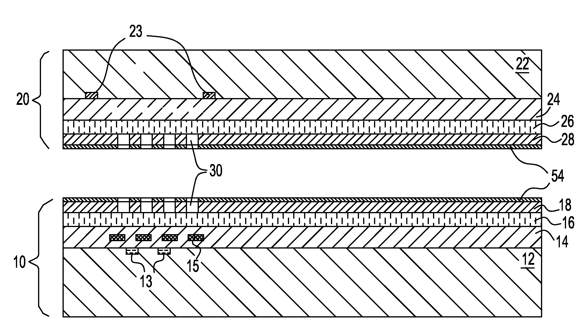
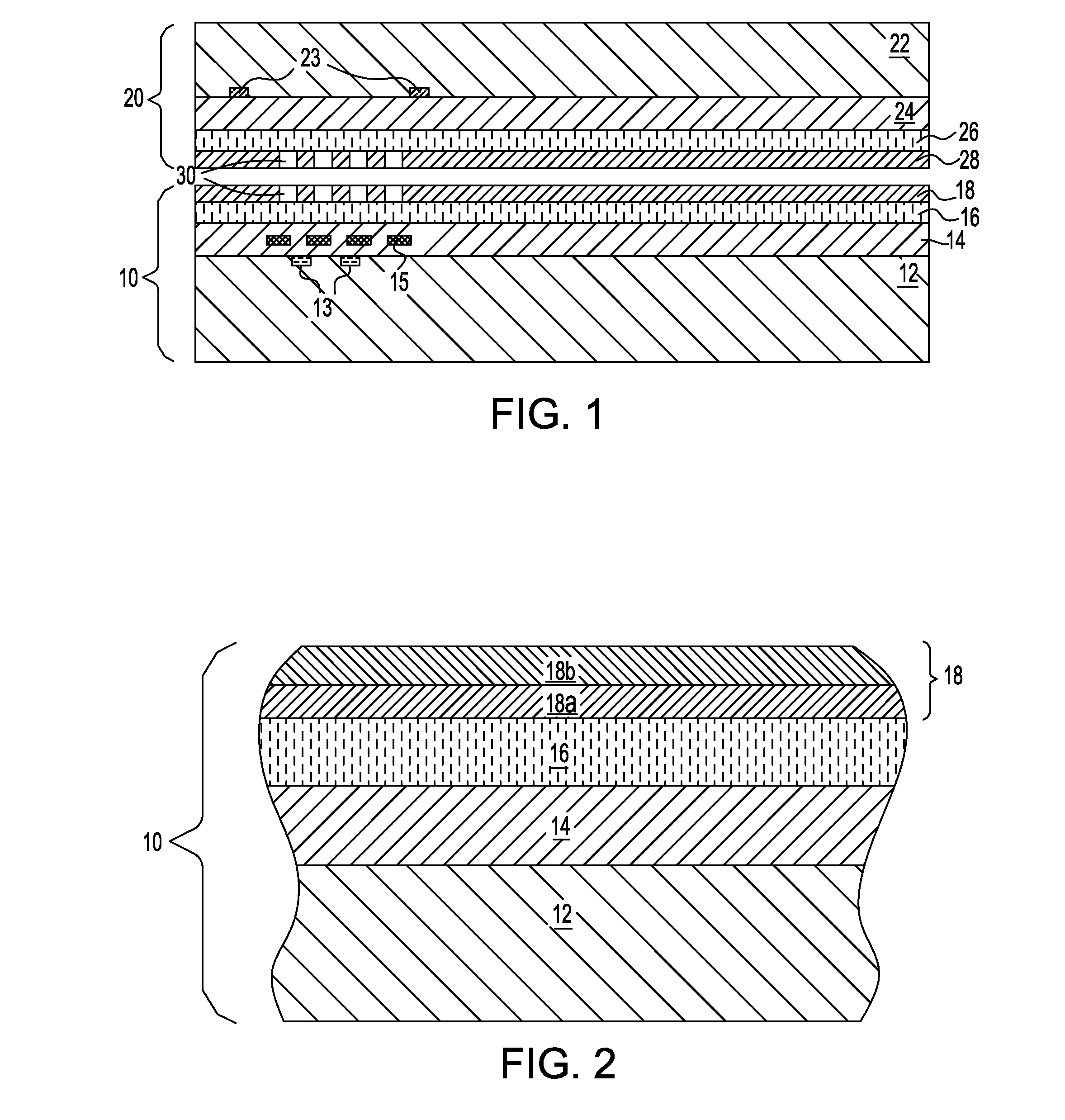
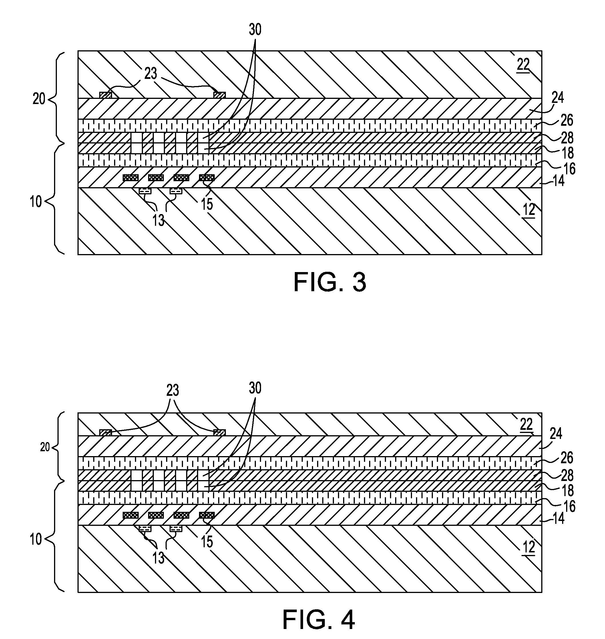
01 Direct bonding techniques for semiconductor wafers
Direct bonding methods involve joining two semiconductor wafers without intermediate adhesive layers. These techniques typically require surface preparation including cleaning, activation, and planarization to achieve atomic-level contact between wafer surfaces. The bonding process may involve room temperature contact followed by thermal annealing to strengthen the bond. This approach is particularly useful for creating silicon-on-insulator structures and three-dimensional integrated circuits.- Direct bonding techniques for semiconductor wafers: Direct bonding methods involve joining two semiconductor wafers without intermediate adhesive layers. These techniques typically require surface preparation including cleaning, activation, and planarization to achieve atomic-level contact between wafer surfaces. The process may involve room temperature bonding followed by annealing at elevated temperatures to strengthen the bond. Surface treatments such as plasma activation or chemical mechanical polishing are commonly employed to enhance bonding quality and reduce defects at the interface.
- Bonding with intermediate layers and adhesives: This approach utilizes intermediate materials between wafers to facilitate bonding. Various adhesive materials including polymers, oxides, or metal layers can be deposited on one or both wafer surfaces prior to bonding. The intermediate layer helps accommodate surface irregularities, reduces thermal stress, and can provide electrical insulation or conduction depending on the application. The bonding process typically involves applying pressure and heat to cure or activate the intermediate material, creating a stable bond between the wafers.
- Wafer alignment and positioning systems: Precise alignment mechanisms are critical for successful wafer bonding, especially for applications requiring accurate pattern registration. Advanced alignment systems employ optical recognition, infrared imaging, or mechanical fixtures to position wafers with sub-micron accuracy. These systems may include real-time monitoring and feedback control to maintain alignment during the bonding process. Specialized chuck designs and vacuum systems help secure wafers in position while allowing for fine adjustments before permanent bonding occurs.
- Thermal management and annealing processes: Temperature control during and after wafer bonding is essential for achieving strong, defect-free bonds. Annealing processes at controlled temperatures strengthen the bond interface by promoting atomic diffusion and eliminating voids. Thermal management strategies include gradual heating and cooling cycles to minimize thermal stress and prevent wafer warping or cracking. Different temperature profiles may be employed depending on the materials being bonded and the desired bond characteristics. Advanced systems may incorporate localized heating or multi-zone temperature control for improved process uniformity.
- Debonding and temporary bonding technologies: Temporary bonding solutions enable processing of thin or fragile wafers by providing mechanical support during fabrication steps, with subsequent controlled debonding. These technologies employ specialized adhesives or bonding materials that can be selectively weakened or removed through thermal, chemical, or mechanical means. The debonding process must be carefully controlled to avoid damage to the processed wafer. Applications include thinning operations, backside processing, and handling of ultra-thin substrates. Various release mechanisms such as laser ablation, thermal slide, or solvent dissolution are utilized depending on the temporary bonding material.
02 Plasma activation and surface treatment for wafer bonding
Surface activation using plasma treatment enhances bonding quality by modifying the surface chemistry and increasing surface energy of semiconductor wafers. Various plasma sources including oxygen, nitrogen, or argon can be employed to create reactive surface groups that facilitate strong bonding at lower temperatures. This method improves bond strength and reduces void formation at the bonding interface, making it suitable for temperature-sensitive applications.Expand Specific Solutions03 Temporary bonding and debonding processes
Temporary bonding technologies enable wafer processing on both sides by providing reversible adhesion between a carrier wafer and a device wafer. These methods utilize specialized adhesive materials or bonding layers that can be removed after processing through thermal, mechanical, or chemical means. This approach is essential for thinning processes, backside processing, and handling of ultra-thin wafers during manufacturing.Expand Specific Solutions04 Hybrid bonding with metal and dielectric interconnections
Hybrid bonding combines both dielectric-to-dielectric and metal-to-metal bonding in a single process step, enabling high-density interconnections between stacked wafers. This technique allows for fine-pitch connections without the need for solder bumps or through-silicon vias. The process involves precise alignment, surface preparation, and controlled annealing to achieve simultaneous bonding of both insulating and conductive regions, which is critical for advanced three-dimensional integration.Expand Specific Solutions05 Void detection and bond quality inspection methods
Quality control techniques for wafer bonding include various inspection methods to detect voids, delamination, and bonding defects at the interface. These methods employ acoustic microscopy, infrared imaging, or other non-destructive testing approaches to evaluate bond integrity. Real-time monitoring during the bonding process and post-bond inspection ensure high yield and reliability of bonded wafer structures, which is essential for commercial production.Expand Specific Solutions
Key Players in Wafer Bonding and 3D Integration Industry
The semiconductor wafer bonding for 3D integration market represents a rapidly evolving sector transitioning from early adoption to mainstream implementation. The industry demonstrates significant growth potential driven by increasing demand for miniaturization and performance enhancement in electronics. Market leaders like Taiwan Semiconductor Manufacturing Co., Intel Corp., and GlobalFoundries showcase mature technological capabilities, while emerging players such as Yangtze Memory Technologies and SMIC-Beijing indicate strong regional development, particularly in Asia. The competitive landscape spans established foundries, specialized equipment manufacturers like Soitec SA with Smart Cut technology, and research institutions including CEA. Technology maturity varies across players, with advanced companies achieving volume production while others focus on R&D and process optimization, creating a dynamic ecosystem supporting diverse 3D integration applications.
Soitec SA
Technical Solution: Soitec specializes in Smart Cut technology for wafer bonding applications, particularly for silicon-on-insulator (SOI) substrates used in 3D integration. Their direct wafer bonding process enables the creation of engineered substrates with precise layer transfer capabilities. Soitec's bonding technology supports various material combinations including silicon, germanium, and compound semiconductors, enabling advanced 3D architectures for RF, power, and photonic applications with excellent interface quality and minimal defect density.
Strengths: Specialized expertise in engineered substrate solutions and material diversity. Weaknesses: Limited to substrate-level applications rather than full 3D integration solutions.
International Business Machines Corp.
Technical Solution: IBM has pioneered several wafer bonding techniques for 3D integration, including oxide-oxide bonding and metal-metal bonding processes. Their approach focuses on through-silicon via (TSV) integration combined with wafer-level bonding for memory and logic stacking applications. IBM's bonding technology achieves high alignment accuracy and supports fine-pitch interconnects, enabling dense 3D architectures for high-performance computing applications with optimized signal integrity and thermal management.
Strengths: Strong research foundation and innovative bonding process development. Weaknesses: Limited commercial manufacturing scale and higher research-focused approach.
Core Patents in Advanced Wafer Bonding Technologies
3D integration structure and method using bonded metal planes
PatentActiveUS20100289144A1
Innovation
- The method involves aligning and bonding metallic layers on two semiconductor structures with an insulator layer, forming a via through the second structure to the first, and filling it with a conductive material, while ensuring the bonded metallic layers are electrically isolated, using materials like copper, nickel, and gold, and employing solid state bonding or solder for the metal-to-metal connection.

Apparatus for manufacturing semiconductor devices
PatentInactiveEP2432007A3
Innovation
- An apparatus comprising a vacuum chamber and a load lock module for precise wafer alignment and bonding under controlled vacuum conditions, using moveable bonding chucks and a control unit to minimize deformation and ensure accurate molecular bonding, reducing edge voids and increasing throughput by avoiding pressure changes between bonding steps.


Thermal Management Challenges in 3D Stacked Devices
Thermal management represents one of the most critical challenges in 3D stacked semiconductor devices, fundamentally altering the heat dissipation paradigm compared to traditional planar architectures. The vertical integration of multiple active layers creates unprecedented thermal density concentrations, where heat generation can exceed 1000 W/cm² in localized regions. This thermal accumulation occurs because conventional heat removal pathways become severely constrained in vertically stacked configurations.
The primary challenge stems from the inherent thermal resistance introduced by wafer bonding interfaces and interlayer dielectric materials. Each bonding layer adds thermal impedance, creating bottlenecks that impede efficient heat conduction to external cooling systems. Silicon dioxide and polymer-based bonding materials typically exhibit thermal conductivities ranging from 0.1 to 1.4 W/mK, significantly lower than silicon's 150 W/mK, creating thermal barriers within the stack.
Vertical heat conduction becomes increasingly problematic as stack height increases, with temperature gradients often exceeding 50°C between bottom and top tiers in high-performance applications. This thermal non-uniformity leads to performance degradation, reliability issues, and potential device failure. The situation is exacerbated by the fact that upper tiers experience reduced cooling efficiency due to their distance from primary heat sinks.
Through-silicon via (TSV) structures, while essential for electrical connectivity, introduce additional thermal complexities. The copper-filled vias can create thermal hot spots due to coefficient of thermal expansion mismatches, while their relatively small cross-sectional areas limit their effectiveness as thermal conduits. The surrounding keep-out zones further restrict available area for dedicated thermal management structures.
Advanced thermal management solutions are emerging to address these challenges, including embedded microfluidic cooling channels, thermal TSVs with enlarged diameters, and novel bonding materials with enhanced thermal conductivity. Integration of phase-change materials and micro-thermoelectric coolers within the stack architecture shows promise for localized thermal regulation.
The thermal design complexity is further compounded by the need to maintain electrical performance while implementing thermal solutions. Power delivery networks must be co-designed with thermal management systems, requiring sophisticated modeling tools that can simultaneously optimize electrical, thermal, and mechanical parameters across the entire 3D structure.
Yield and Reliability Considerations in Wafer Bonding
Yield and reliability represent critical performance metrics that determine the commercial viability of wafer bonding processes in 3D integration applications. The bonding yield directly correlates with manufacturing costs, as defective bonds result in chip failures and reduced production efficiency. Reliability considerations encompass both short-term bond integrity and long-term performance under operational stress conditions, including thermal cycling, mechanical stress, and environmental exposure.
Defect mechanisms significantly impact bonding yield, with particle contamination being the primary contributor to bond failures. Sub-micron particles trapped at the bonding interface create localized stress concentrations that prevent proper atomic-level contact formation. Surface roughness variations exceeding critical thresholds also compromise bond uniformity, leading to incomplete bonding areas that manifest as yield losses during electrical testing phases.
Thermal stress management emerges as a fundamental reliability challenge due to coefficient of thermal expansion mismatches between bonded materials. Silicon-to-silicon bonds typically exhibit superior thermal compatibility compared to heterogeneous material combinations. The accumulated stress during temperature excursions can induce interfacial delamination or crack propagation, particularly at bond peripheries where stress concentration factors are highest.
Process parameter optimization plays a crucial role in achieving acceptable yield levels. Bonding temperature, applied pressure, and ambient atmosphere control must be precisely calibrated to ensure consistent bond formation across entire wafer surfaces. Statistical process control methodologies enable real-time monitoring of critical parameters, facilitating rapid identification of process deviations that could compromise yield performance.
Reliability testing protocols incorporate accelerated stress testing to evaluate long-term bond stability under simulated operational conditions. Temperature cycling tests, typically ranging from -40°C to 150°C, assess thermal fatigue resistance over thousands of cycles. Mechanical stress testing through controlled bending or vibration exposure validates bond robustness under physical loading conditions encountered in packaging and assembly operations.
Quality assurance methodologies integrate both destructive and non-destructive evaluation techniques to characterize bond integrity. Acoustic microscopy enables detection of interfacial voids or delamination areas without sample destruction, while cross-sectional analysis provides detailed interfacial microstructure characterization. These complementary approaches establish comprehensive quality metrics that correlate with field reliability performance, enabling predictive yield modeling and process optimization strategies.
Unlock deeper insights with Patsnap Eureka Quick Research — get a full tech report to explore trends and direct your research. Try now!
Generate Your Research Report Instantly with AI Agent
Supercharge your innovation with Patsnap Eureka AI Agent Platform!