

Wire Bonding vs Flip-Chip: Semiconductor Packaging Efficiency
MAR 31, 20269 MIN READ
Generate Your Research Report Instantly with AI Agent
PatSnap Eureka helps you evaluate technical feasibility & market potential.
Semiconductor Packaging Evolution and Efficiency Goals
Semiconductor packaging has undergone remarkable transformation since the inception of integrated circuits in the 1960s. The evolution began with simple dual in-line packages (DIPs) and ceramic packages that prioritized functionality over miniaturization. As semiconductor devices became more complex and performance demands intensified, packaging technologies evolved from through-hole mounting to surface-mount technology, fundamentally changing how chips interface with circuit boards.
The transition from wire bonding to flip-chip technology represents one of the most significant paradigm shifts in packaging evolution. Wire bonding, introduced in the early days of semiconductor manufacturing, established the foundation for chip-to-substrate connections through fine metal wires. This technology dominated the industry for decades due to its reliability, cost-effectiveness, and manufacturing simplicity.
Flip-chip technology emerged as a revolutionary alternative in the 1960s, initially developed by IBM, but gained widespread adoption only in recent decades. This approach inverts the traditional packaging concept by placing the chip face-down and creating direct electrical connections through solder bumps or copper pillars, eliminating the need for wire bonds entirely.
The driving forces behind packaging evolution center on achieving superior electrical performance, enhanced thermal management, and increased miniaturization. Modern applications demand higher I/O density, reduced signal propagation delays, and improved power delivery efficiency. These requirements have pushed the industry toward advanced packaging solutions that can accommodate shrinking form factors while maintaining or improving performance metrics.
Current efficiency goals focus on several critical parameters including electrical performance optimization, thermal dissipation enhancement, and manufacturing cost reduction. Signal integrity has become paramount as operating frequencies increase and noise margins decrease. Packaging solutions must minimize parasitic inductance and capacitance while providing robust power distribution networks.
Thermal management represents another crucial efficiency target, as higher transistor densities generate increased heat flux. Effective heat removal directly impacts device reliability, performance stability, and operational lifespan. Modern packaging approaches must integrate sophisticated thermal pathways and heat spreading mechanisms.
The industry also pursues manufacturing scalability and cost optimization. Packaging technologies must demonstrate economic viability across high-volume production while maintaining quality standards and yield rates. This balance between performance enhancement and cost control continues to drive innovation in both wire bonding and flip-chip methodologies.
Market Demand for Advanced Packaging Solutions
The semiconductor packaging industry is experiencing unprecedented demand driven by the proliferation of high-performance computing applications, artificial intelligence processors, and advanced mobile devices. Traditional packaging methods are increasingly challenged by requirements for higher I/O density, improved thermal management, and enhanced electrical performance. This market pressure has intensified the evaluation between wire bonding and flip-chip technologies, as manufacturers seek optimal solutions for next-generation semiconductor products.
Consumer electronics continue to dominate packaging demand, with smartphones, tablets, and wearable devices requiring increasingly compact and efficient packaging solutions. The automotive sector represents another significant growth driver, particularly with the expansion of electric vehicles and autonomous driving systems that demand robust, high-reliability packaging capable of withstanding harsh operating environments. These applications favor advanced packaging technologies that can deliver superior performance while maintaining cost-effectiveness.
Data center and cloud computing infrastructure development has created substantial demand for high-performance processors requiring advanced packaging solutions. Graphics processing units, central processing units, and specialized AI accelerators increasingly rely on sophisticated packaging technologies to achieve required performance levels. The growing complexity of these applications has shifted market preference toward packaging solutions offering superior thermal dissipation and electrical characteristics.
The Internet of Things ecosystem presents unique packaging challenges, requiring solutions that balance performance, power consumption, and cost constraints. Edge computing devices, sensor networks, and connected appliances demand packaging technologies capable of supporting diverse functional requirements while maintaining manufacturing scalability. This market segment particularly values packaging solutions offering flexibility in design implementation and cost optimization.
Emerging applications in 5G telecommunications, augmented reality, and quantum computing are creating new packaging requirements that traditional technologies struggle to address. These applications demand ultra-high frequency performance, minimal signal loss, and exceptional thermal management capabilities. Market demand increasingly favors packaging technologies capable of supporting these advanced performance requirements while enabling continued miniaturization trends.
The competitive landscape reflects growing market sophistication, with customers increasingly evaluating packaging solutions based on total system performance rather than individual component metrics. This shift has elevated the importance of packaging efficiency considerations, driving demand for solutions that optimize the balance between electrical performance, thermal management, manufacturing complexity, and overall cost-effectiveness across diverse application scenarios.
Current Wire Bonding vs Flip-Chip Technology Status
Wire bonding remains the dominant interconnection technology in semiconductor packaging, accounting for approximately 85% of all packaged semiconductors globally. This mature technology utilizes thin metal wires, typically gold or copper, to create electrical connections between the die and package substrate. Current wire bonding systems achieve placement accuracies of ±2-3 micrometers and can operate at speeds exceeding 15 wires per second for high-volume production.
The technology has evolved significantly with the introduction of copper wire bonding, which offers cost advantages over traditional gold wire while maintaining comparable electrical performance. Advanced wire bonding equipment now incorporates features such as automatic wire tail length control, real-time loop height monitoring, and adaptive bonding parameter adjustment based on die characteristics.
Flip-chip technology represents a more advanced packaging approach, currently capturing approximately 15% of the semiconductor packaging market but growing rapidly at 8-12% annually. This technology eliminates wire bonds by directly connecting the die to the substrate through solder bumps or copper pillars. Modern flip-chip processes achieve bump pitches as fine as 40 micrometers with placement accuracies of ±5 micrometers.
Contemporary flip-chip implementations utilize various interconnection methods including lead-free solder bumps, copper pillar bumps, and micro-bumps for 3D stacking applications. The underfill process has become increasingly sophisticated, with capillary underfill materials achieving glass transition temperatures above 150°C and coefficients of thermal expansion closely matched to silicon substrates.
Current flip-chip technology faces challenges in thermal management and mechanical reliability, particularly for large die applications. Advanced thermal interface materials and innovative substrate designs are being deployed to address these limitations. The technology demonstrates superior electrical performance with reduced parasitic inductance and capacitance compared to wire bonding.
Manufacturing infrastructure for both technologies continues to advance, with wire bonding equipment achieving higher throughput through multi-head configurations and flip-chip systems incorporating advanced vision systems for precise bump placement. The choice between technologies increasingly depends on specific application requirements, cost considerations, and performance targets rather than fundamental technical limitations.
Existing Wire Bonding and Flip-Chip Solutions
01 Flip-chip packaging with enhanced thermal and electrical performance
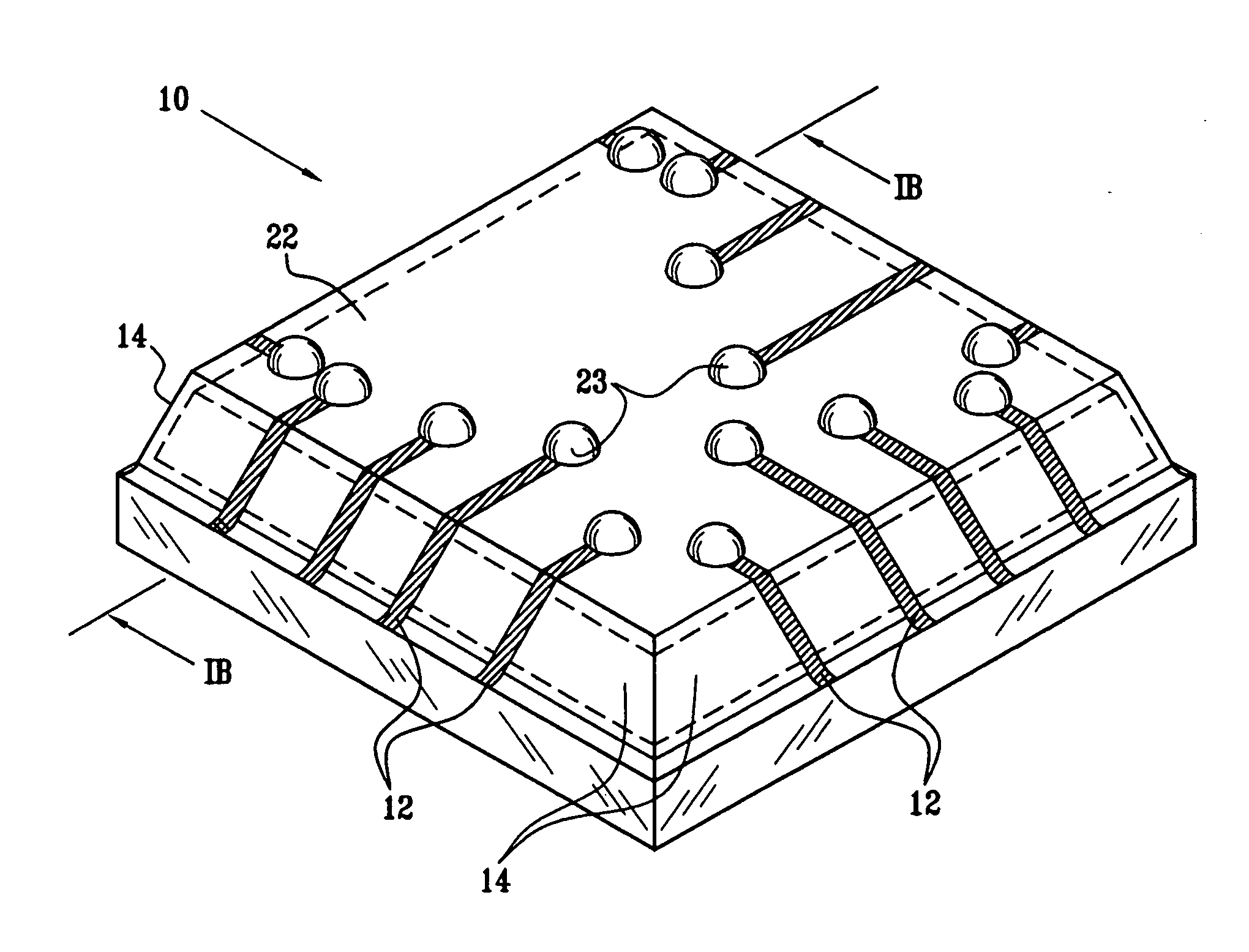
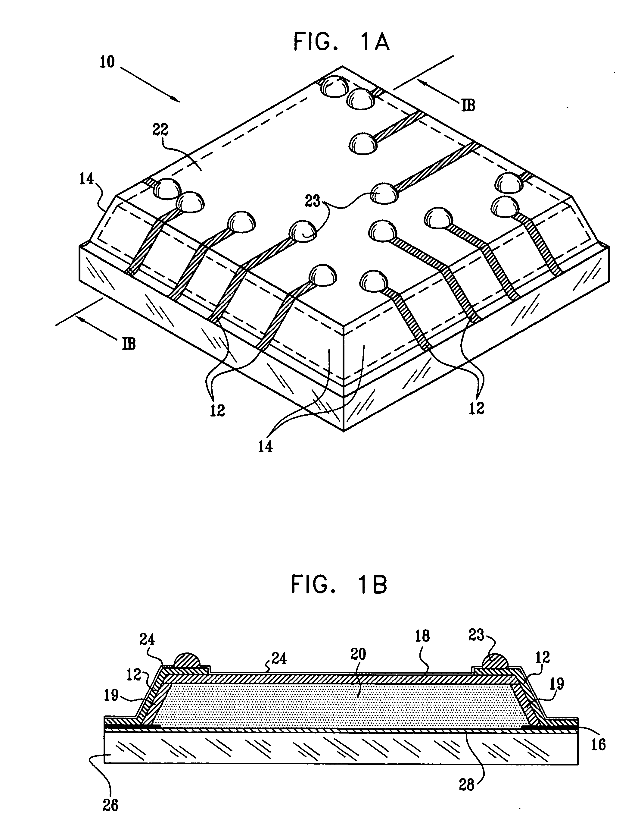
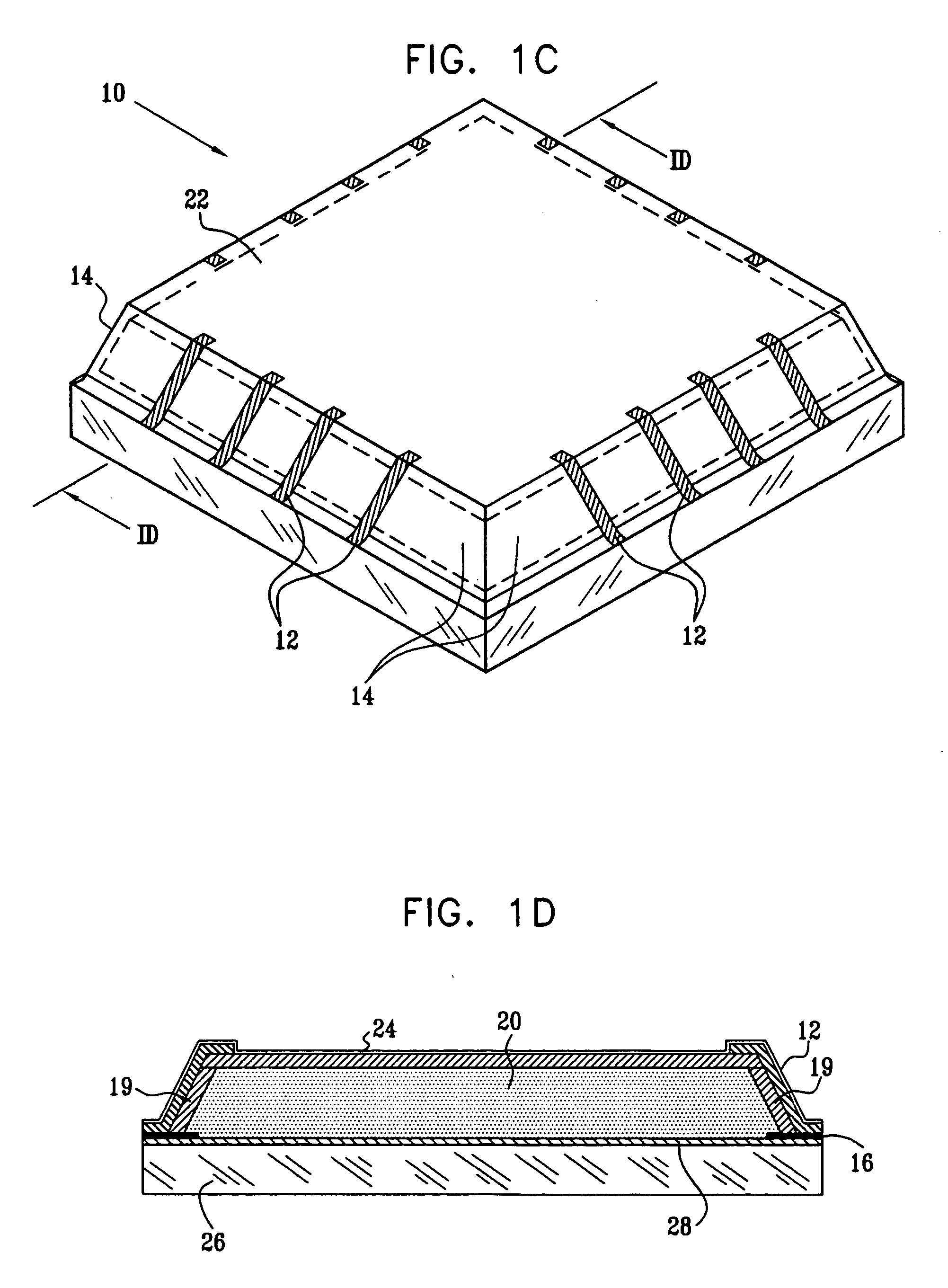
Flip-chip packaging technology provides superior thermal dissipation and electrical performance compared to traditional wire bonding. The direct connection between chip and substrate through solder bumps reduces electrical path length and thermal resistance, enabling higher frequency operation and better heat management. This approach eliminates the need for wire loops, resulting in more compact package designs with improved signal integrity and reduced parasitic effects.- Flip-chip packaging with underfill materials for enhanced reliability: Flip-chip packaging technology utilizes underfill materials between the chip and substrate to improve mechanical strength, thermal performance, and reliability. This approach provides better stress distribution and protection against environmental factors compared to traditional wire bonding methods. The underfill process enhances the overall package integrity and extends the operational lifetime of semiconductor devices.
- Wire bonding process optimization for high-density interconnections: Advanced wire bonding techniques focus on optimizing bond pad layouts, wire loop profiles, and bonding parameters to achieve higher interconnection density and improved electrical performance. These methods address challenges in fine-pitch applications and enable cost-effective packaging solutions for various semiconductor devices. Process improvements include automated bonding equipment and enhanced quality control measures.
- Hybrid packaging combining wire bonding and flip-chip technologies: Hybrid packaging approaches integrate both wire bonding and flip-chip techniques within a single package to leverage the advantages of each method. This combination allows for flexible design options, optimized cost-performance ratios, and accommodation of different chip types in multi-chip modules. The hybrid approach provides solutions for complex packaging requirements where single-method limitations exist.
- Thermal management comparison between packaging methods: Thermal dissipation efficiency differs significantly between wire bonding and flip-chip packaging architectures. Flip-chip configurations typically offer superior heat transfer paths through direct chip-to-substrate contact, while wire bonding relies on alternative thermal pathways. Design considerations include thermal interface materials, heat spreaders, and package geometry optimization to meet thermal performance requirements for high-power applications.
- Manufacturing throughput and cost efficiency analysis: Production efficiency varies between wire bonding and flip-chip processes based on equipment requirements, cycle times, and yield considerations. Wire bonding generally offers lower initial capital investment and simpler process control, while flip-chip provides higher throughput for mass production and reduced package footprint. Cost-effectiveness depends on application volume, performance requirements, and manufacturing infrastructure capabilities.
02 Hybrid bonding approaches combining wire bonding and flip-chip
Hybrid packaging methods integrate both wire bonding and flip-chip technologies to optimize manufacturing efficiency and cost-effectiveness. These approaches allow selective use of each technology based on specific connection requirements, enabling manufacturers to balance performance benefits with production costs. The hybrid method provides flexibility in addressing different I/O density requirements and thermal management needs within a single package.Expand Specific Solutions03 Wire bonding process optimization for high-volume manufacturing
Advanced wire bonding techniques focus on improving throughput and reliability in high-volume production environments. Optimizations include automated bonding equipment, improved wire materials, and enhanced bonding parameters to reduce cycle time while maintaining connection quality. These improvements address manufacturing efficiency concerns while preserving the cost advantages and flexibility of wire bonding technology.Expand Specific Solutions04 Flip-chip underfill and reliability enhancement
Underfill materials and processes are critical for flip-chip package reliability and long-term performance. Advanced underfill techniques improve mechanical strength, reduce thermal stress, and enhance moisture resistance of flip-chip assemblies. These enhancements address reliability concerns associated with flip-chip technology, making it more competitive for applications requiring high durability and extended operational lifetimes.Expand Specific Solutions05 Cost and yield comparison between packaging technologies
Economic analysis of wire bonding versus flip-chip packaging considers equipment costs, material expenses, yield rates, and throughput capabilities. Wire bonding typically offers lower initial investment and greater process flexibility, while flip-chip provides advantages in high-density applications and performance-critical designs. Manufacturing yield optimization and defect reduction strategies are essential for both technologies to achieve competitive cost structures in different market segments.Expand Specific Solutions
Major Semiconductor Packaging Industry Players
The semiconductor packaging industry is experiencing a critical transition phase, with wire bonding and flip-chip technologies representing different maturity levels in a rapidly expanding market valued at over $25 billion globally. Wire bonding remains the dominant mature technology due to its cost-effectiveness and reliability, while flip-chip packaging is gaining momentum for high-performance applications requiring superior electrical and thermal characteristics. Technology leaders like Taiwan Semiconductor Manufacturing Co., Samsung Electronics, and Advanced Semiconductor Engineering demonstrate varying degrees of flip-chip adoption, with TSMC and Samsung leading advanced packaging innovations. Traditional packaging specialists including Siliconware Precision Industries, Powertech Technology, and ASE Group are investing heavily in flip-chip capabilities to serve growing demand from mobile, automotive, and AI applications. The competitive landscape shows established players like Texas Instruments and Infineon Technologies balancing both technologies based on application requirements, while emerging companies such as Huatian Technology are expanding flip-chip services to capture market share in this evolving ecosystem.
Taiwan Semiconductor Manufacturing Co., Ltd.
Technical Solution: TSMC employs advanced flip-chip packaging technology for high-performance processors and mobile SoCs, utilizing copper pillar bumps and through-silicon vias (TSVs) for enhanced electrical performance. Their CoWoS (Chip-on-Wafer-on-Substrate) technology integrates flip-chip bonding with 2.5D/3D packaging solutions, enabling higher bandwidth and reduced form factors. For cost-sensitive applications, TSMC maintains wire bonding capabilities using gold and copper wire technologies with optimized loop profiles to minimize parasitic effects and improve signal integrity in automotive and IoT devices.
Strengths: Industry-leading flip-chip technology with superior electrical performance and miniaturization capabilities. Weaknesses: Higher costs compared to traditional wire bonding solutions, requiring significant capital investment.
Samsung Electronics Co., Ltd.
Technical Solution: Samsung implements both wire bonding and flip-chip technologies across their semiconductor portfolio. Their flip-chip solutions feature advanced underfill materials and micro-bump technology for mobile processors and memory devices, achieving pitch sizes down to 40μm. For memory packaging, Samsung utilizes wire bonding with optimized bond pad designs and low-loop profiles to reduce package height while maintaining reliability. Their packaging roadmap focuses on heterogeneous integration combining both technologies based on performance requirements and cost targets for different market segments.
Strengths: Comprehensive packaging portfolio with strong flip-chip capabilities for high-end applications. Weaknesses: Complex supply chain management required for dual-technology approach, potentially higher development costs.
Core Patents in Advanced Packaging Technologies
Methods and apparatus for packaging integrated circuit devices
PatentInactiveUS20050104179A1
Innovation
- The development of integrally packaged optronic integrated circuit devices with a crystalline substrate having planar surfaces and edge surfaces, featuring a chip scale packaging layer made of materials like glass, quartz, or sapphire, and electrical conductors connected directly to pads on the planar surfaces, along with insulation layers and spectral filters, to create a compact and radiation-transparent protective structure.

Packaging substrate having embedded semiconductor chip
PatentInactiveUS20110031606A1
Innovation
- The use of reinforcing dielectric layers made of materials like glass fiber to enhance the structural support and prevent recess formation between the semiconductor chip and the cavity, thereby preventing delamination and warpage, and ensuring reliable electrical connections through the incorporation of conductive vias and wiring layers.


Manufacturing Cost Analysis for Packaging Methods
The manufacturing cost structure for wire bonding and flip-chip packaging methods reveals significant differences across multiple cost components. Wire bonding demonstrates lower initial capital investment requirements, with equipment costs typically ranging from $200,000 to $500,000 per production line. The process utilizes relatively simple machinery and requires minimal clean room infrastructure compared to flip-chip alternatives.
Flip-chip packaging demands substantially higher upfront investments, with equipment costs often exceeding $2-5 million per production line. Advanced lithography systems, precision placement equipment, and sophisticated underfill dispensing systems contribute to elevated capital expenditure. However, this higher initial investment translates into superior throughput capabilities and reduced per-unit processing time.
Labor costs present contrasting profiles between the two methodologies. Wire bonding requires skilled operators for die attachment, wire placement, and quality inspection, resulting in higher labor intensity per unit. The sequential nature of wire placement limits automation potential, maintaining dependency on manual intervention. Conversely, flip-chip processes achieve higher automation levels, reducing direct labor requirements per unit while demanding more specialized technical expertise for equipment maintenance and process optimization.
Material costs favor wire bonding in terms of consumables, with gold or copper wires representing relatively low-cost inputs. Flip-chip packaging requires expensive solder bumps, underfill materials, and specialized substrates, increasing material costs by 15-30% compared to wire bonding alternatives. However, flip-chip's elimination of wire bonds reduces package size, potentially offsetting material cost increases through improved substrate utilization efficiency.
Yield considerations significantly impact overall manufacturing economics. Wire bonding typically achieves 95-98% yield rates with mature process control, while flip-chip processes may experience 90-95% yields due to increased complexity in bump formation and placement accuracy requirements. Quality control costs are higher for flip-chip due to more sophisticated inspection requirements and potential rework complexity.
Throughput analysis reveals flip-chip's advantage in high-volume production scenarios. While wire bonding processes individual connections sequentially, flip-chip enables parallel connection formation, reducing cycle times by 40-60% for complex devices with high I/O counts. This throughput advantage becomes increasingly significant as pin counts exceed 200-300 connections per package.
Thermal Management in High-Density Packaging
Thermal management represents one of the most critical challenges in modern semiconductor packaging, particularly when comparing wire bonding and flip-chip technologies in high-density applications. The fundamental difference in thermal pathways between these two approaches significantly impacts overall packaging efficiency and device reliability.
Wire bonding technology faces inherent thermal limitations due to its vertical interconnect structure. Heat generated by the semiconductor die must travel through the substrate and package body to reach external heat sinks. This thermal path creates substantial resistance, leading to elevated junction temperatures and potential hot spots. The wire bonds themselves, typically made of gold or aluminum, provide minimal thermal conductivity contribution, forcing reliance on alternative heat dissipation routes.
Flip-chip packaging offers superior thermal performance through direct die-to-substrate contact. The solder bumps or copper pillars create multiple thermal pathways, enabling more efficient heat transfer from the active silicon surface directly to the package substrate. This configuration reduces thermal resistance by approximately 30-50% compared to wire bonding, allowing for higher power densities and improved performance margins.
Advanced thermal management solutions have emerged to address high-density packaging requirements. Thermal interface materials with enhanced conductivity, integrated heat spreaders, and embedded cooling channels represent key innovations. For flip-chip applications, underfill materials with improved thermal properties help distribute heat more effectively across the die area.
Package-level thermal design considerations include substrate material selection, via density optimization, and thermal pad configurations. High-density packaging demands careful attention to thermal coupling between adjacent components, requiring sophisticated modeling and simulation tools to predict temperature distributions and identify potential failure modes.
The evolution toward system-in-package and 3D integration amplifies thermal management complexity. Multi-die configurations create thermal interference patterns that traditional single-die thermal models cannot accurately predict. Advanced packaging technologies increasingly rely on active cooling solutions, including micro-channel cooling and thermoelectric devices, to maintain acceptable operating temperatures in high-performance applications.
Unlock deeper insights with PatSnap Eureka Quick Research — get a full tech report to explore trends and direct your research. Try now!
Generate Your Research Report Instantly with AI Agent
Supercharge your innovation with PatSnap Eureka AI Agent Platform!