
Electronic package of light-sensitive semiconductor device and manufacturing and assembling method
A light sensing and semiconductor technology, applied in semiconductor devices, electric solid state devices, circuits, etc., can solve the problems of yield loss, complexity of structure and manufacturing process, and high cost
Patent Information
- Authority / Receiving Office
- CN · China
- Patent Type
- Patents(China)
- Current Assignee / Owner
- Publication Date
- 2009-03-25
Smart Images
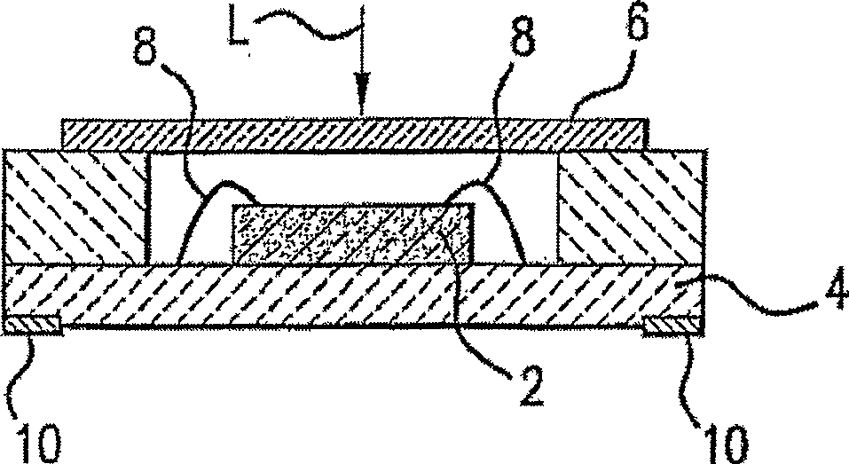
Figure 1 
Figure 2 
Figure 3
Abstract
Description
technical field
[0001] The present invention generally relates to an electronic package of a semiconductor integrated circuit, and more particularly, relates to an electronic package of a photosensitive semiconductor device. Background technique
[0002] Light-sensitive semiconductor devices are usually mounted in ceramic packages. figure 1 A schematic cross-sectional view of a ceramic leadless chip carrier (CLCC), which is the most common form of packaging for light-sensing devices, is shown. As shown in the figure, inside the area covered by the glass cover 6 , the light-sensing semiconductor chip is fixed on the ceramic substrate 4 with the front facing up by using epoxy material or similar material. Soldering wires 8 are generally used to connect the photosensitive chip 2 to the ceramic substrate 4 . Solderable pads 10 are provided on the bottom of the ceramic substrate 4 to connect the package to a circuit board.
[0003] Perhaps the most important drawback of this p...
Examples
Embodiment Construction
[0031] A photosensitive semiconductor wafer has a plurality of chips and, as in other semiconductor wafers, each chip has an integrated circuit formed on the front side of the wafer. Each chip has multiple bonding pads. The front side of the wafer has a patterned passivation layer to protect the underlying integrated circuits. There is an opening in the passivation layer on the welding pad. Each such photosensitive chip has at least one photosensitive area on the front side.
[0032]Wafer bumping technology is well known (as described in US Patent No. 3,292,240, later assigned to IBM, entitled "Method of Fabricating Microfunctional Components"), and has been widely used since its inception. A typical wafer bumping process includes at least one patterned metal layer to form solder bump pads that are attached to the pads of the wafer. Alloys used for solder bump pads are usually referred to as under-bump alloys (UBM) and are often multilayered to provide multiple functions su...