
Boron nitride pyrolyzing crucible coating method
A crucible and surface technology, applied in the field of PBN crucible surface treatment, can solve the problems of increasing industrial production cost, layering, and not being able to solve the service life of PBN crucible well
Patent Information
- Authority / Receiving Office
- CN · China
- Patent Type
- Patents(China)
- Current Assignee / Owner
- Publication Date
- 2009-06-03
Smart Images
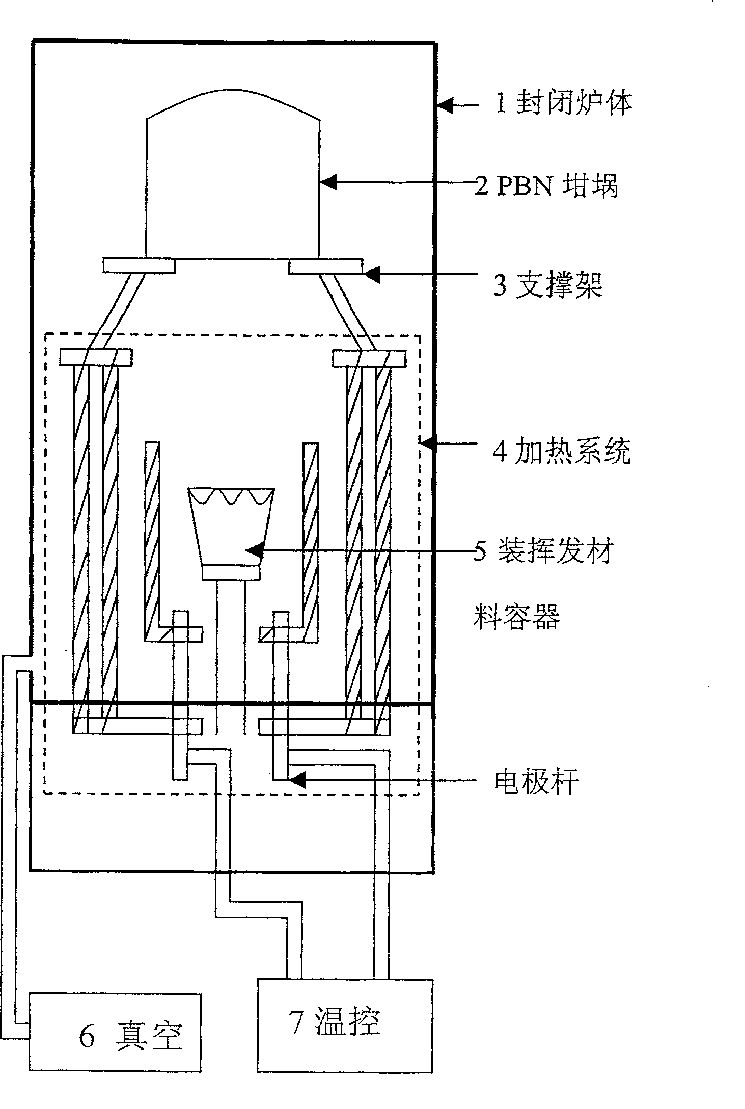
Figure 1
Abstract
Description
technical field
[0001] The invention belongs to the technical field of semiconductors, in particular to a method and a device for treating the surface layer of a PBN crucible in the preparation process for growing bulk single crystals by the LEC method. Background technique
[0002] Semiconductor materials are the foundation of the information society and are widely used in the fields of electronic information and optical communications. III-V compound semiconductor materials occupy an important position in the cutting-edge scientific field due to their specific properties, among which gallium arsenide and indium phosphide are used as the basis for the development of ultra-high-speed integrated circuits, microwave monolithic circuits, optoelectronic devices and their optoelectronic integration Materials have received a lot of attention.
[0003] In the early 1980s, the LEC technology was developed internationally, that is, in the high-pressure single crystal furnace, the ra...
Examples
Embodiment Construction
[0020] see figure 1 Shown, the PBN crucible surface coating of the present invention comprises:
[0021] 1. Equipment
[0022] The container (5) for containing the volatile material is located in the center of the closed furnace chamber (1), and is made of high temperature resistant material, which does not react with the volatile material. Volatile materials can form a thin film on the surface of the PBN(2) crucible without affecting the quality of the bulk single crystal. The PBN (2) crucible is on the support system (3) at the top of the closed furnace chamber (1).
[0023] A set of heating system (4) and temperature control equipment (7) are used to heat up the temperature, so that the volatile material is diffused to the surface layer of the PBN crucible for deposition. The heating system (4) is around the closed furnace chamber (1).
[0024] A support system (3) supports the PBN crucible (2) and requires high temperature resistance.
[0025] A closed furnace chamber...