
Method and structure for molding leadframe strip
A lead frame strip and lead frame technology is applied in the fields of semiconductor devices, semiconductor/solid-state device manufacturing, semiconductor/solid-state device components, etc., and can solve the problems of difficult output per unit time, waste of lead frame strip 1 space, etc.
Patent Information
- Authority / Receiving Office
- CN · China
- Patent Type
- Patents(China)
- Current Assignee / Owner
- Publication Date
- 2013-03-27
Smart Images
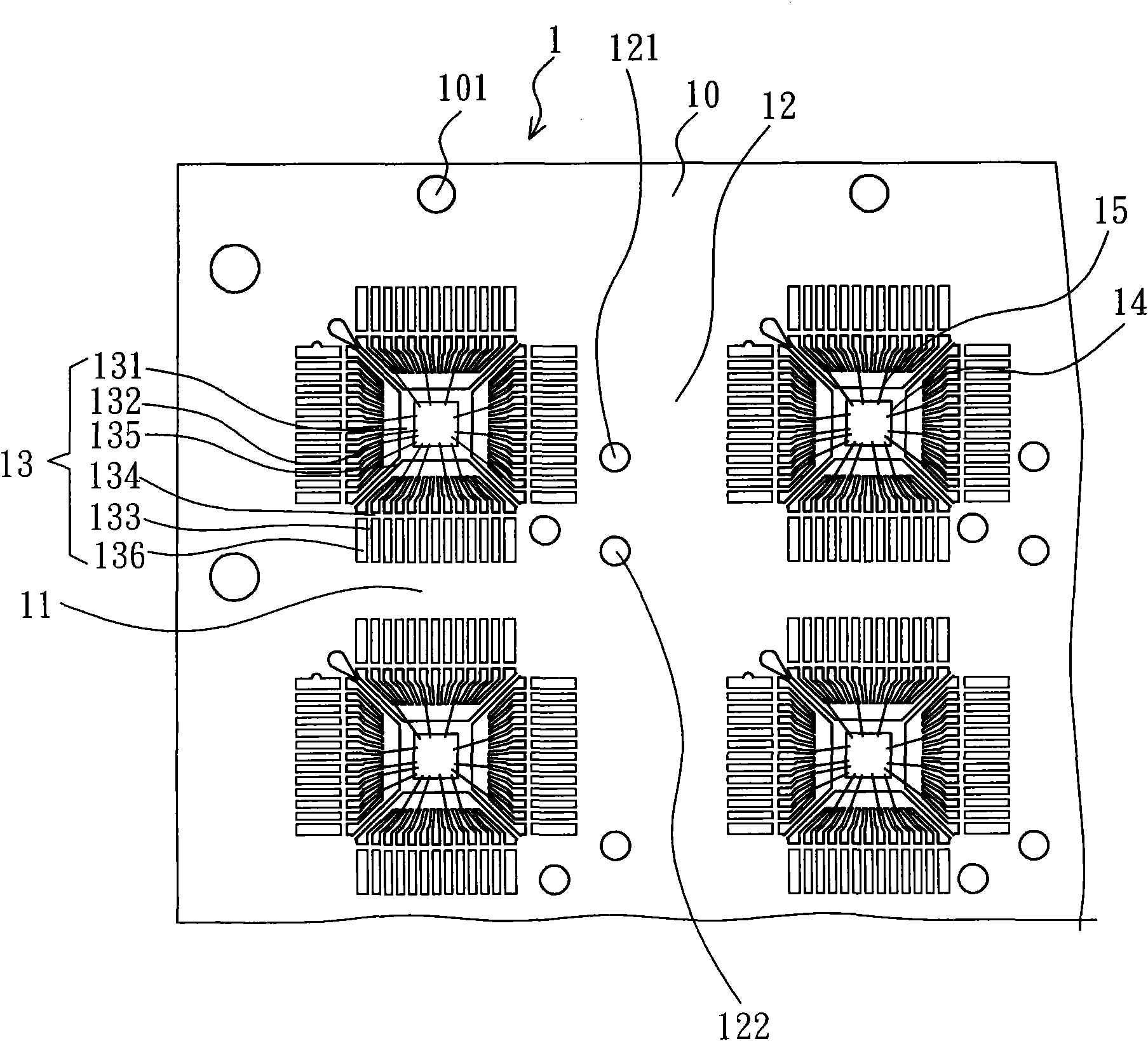
Figure 1 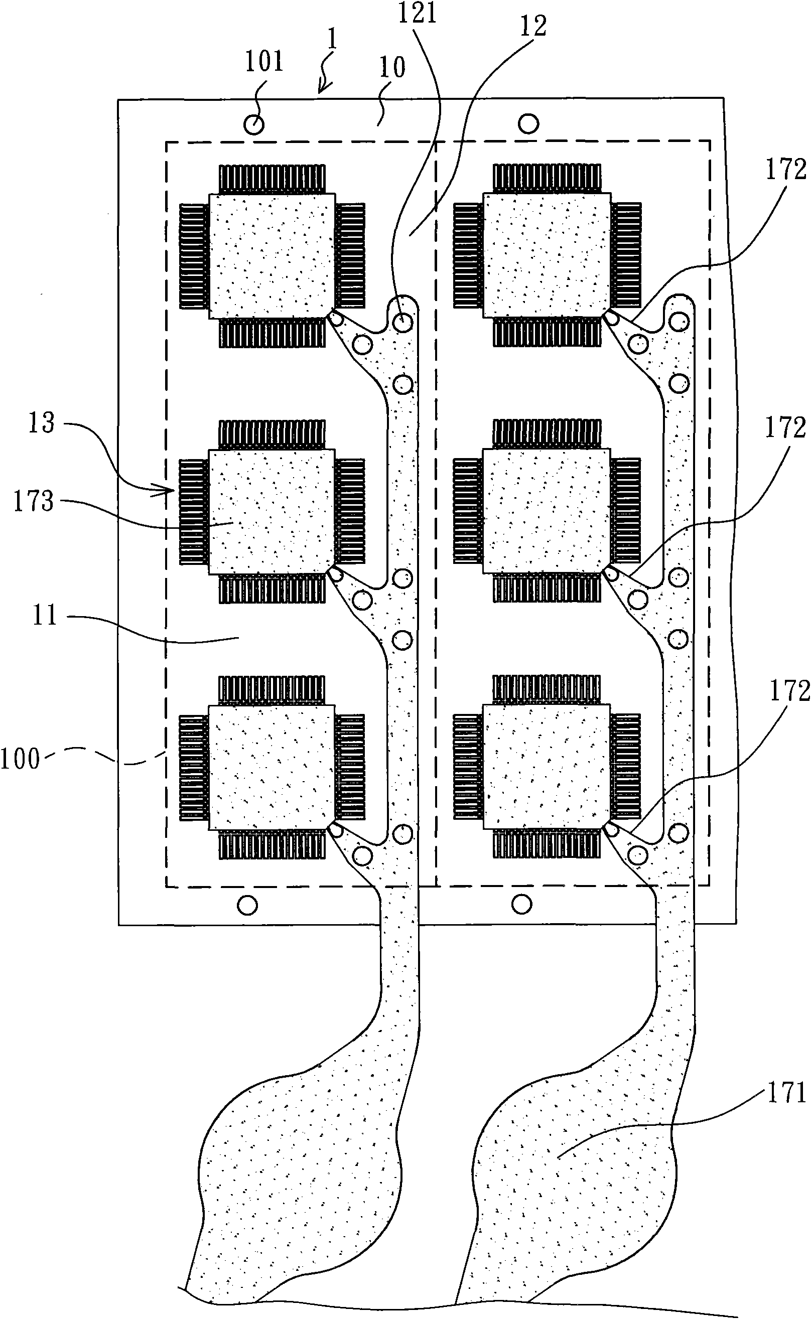
Figure 2 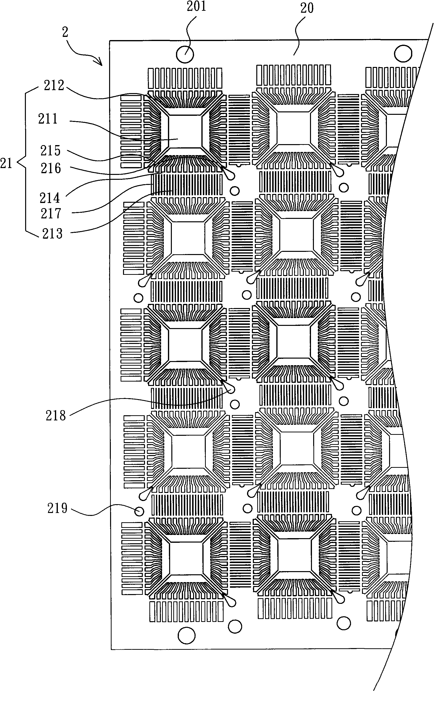
Figure 3
Abstract
Description
Technical field
[0001] The present invention relates to a sealing method and sealing structure for lead frame strips, in particular to a method that can increase the output per unit time (units per hour, UPH) and relatively reduce the problem of mold flow punching. The sealing method and sealing structure of QFP lead frame strips.
Background technique
[0002] Nowadays, in order to meet various packaging requirements, the semiconductor packaging industry has gradually developed various types of packaging structures. Among them, silicon chips (chips) cut from semiconductor silicon wafers (wafers) are usually firstly processed by wire bonding. ) or bumping (bumping) and other appropriate methods to select and fix on the leadframe (leadframe) or substrate (substrate), and then use the encapsulation gel to encapsulate and protect the silicon chip, so that the basic structure of a semiconductor package structure can be completed. Common package structures with lead frames in...
Examples
Embodiment Construction
[0031] In order to make the above objects, features and advantages of the present invention more comprehensible, preferred embodiments of the present invention are exemplified below and described in detail in conjunction with the accompanying drawings. Furthermore, the directional terms mentioned in the present invention, such as "up", "down", "front", "back", "left", "right", "inside", "outside" or "side", etc., It is only for orientation with reference to the attached drawings. Therefore, the directional terms used are used to illustrate and understand the present invention, but not to limit the present invention.
[0032] Please refer to image 3 and 4 As shown, the sealing method and sealing structure of lead frame strips according to the first embodiment of the present invention are mainly used in the manufacture of semiconductor packaging products with four rows of lead frames, for example, in the manufacture of quad flat packages (quad flat packages, QFP), square fla...