
Infrared absorption structure and uncooled infrared detector based on infrared absorption structure
An infrared absorption and non-cooling technology, applied in the field of thermal radiation infrared detection, can solve the problems of poor uniformity of infrared response, and achieve the effects of eliminating poor uniformity of infrared response, high infrared absorption, and high utilization rate of radiation energy
Patent Information
- Authority / Receiving Office
- CN · China
- Patent Type
- Patents(China)
- Current Assignee / Owner
- Publication Date
- 2012-12-19
- Estimated Expiration
- Not applicable · inactive patent
Smart Images
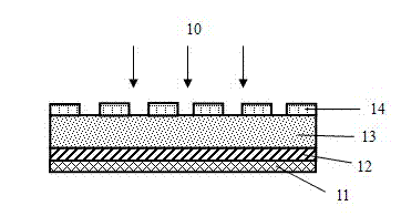
Figure 1 
Figure 2 
Figure 3
Abstract
Description
technical field
[0001] The invention belongs to thermal radiation infrared detection technology, in particular to a multi-layer infrared absorption structure with low thermal mass, wide angle and high infrared absorption rate and a non-cooling infrared detector based on the structure. Background technique
[0002] Uncooled infrared detectors use the thermal infrared radiation of target objects for target detection. The principle is that the photosensitive area of the infrared detector absorbs the thermal infrared radiation incident from the outside to increase the temperature of the photosensitive element itself. The temperature-increased photosensitive element converts its own temperature change into a certain physical, chemical or electrical characteristic change of its properties and forms a detection through an external detection system. Compared with cooled infrared detectors, uncooled infrared detectors have the advantages of low price, small size, light weight, and...
Examples
Embodiment Construction
[0024] A detailed description of the infrared absorbing structure and detector of the present invention is given below.
[0025] Such as figure 1 As shown, a typical infrared absorbing structure provided by the present invention includes a bottom infrared reflective layer 11 , a first insulating layer 12 , an infrared sensitive layer 13 and a surface structure layer 14 stacked in sequence against the incident direction of infrared radiation. A beam of infrared radiation 10 is incident from the surface structure layer 14 into the infrared absorbing structure.
[0026] The bottom infrared reflective layer 11 can be a metal material with high electrical conductivity σ or low resistivity ρ (ρ=1 / σ), or a metal compound with high electrical conductivity, or a highly doped semiconductor material, and the high electrical conductivity is Refers to resistivity ≤ 10mΩ cm, high doping refers to free carrier concentration ≥ 1 × 10 19 cm -3 . Metal materials such as gold, silver or alum...